國 立 交 通 大 學
電信工程學系
博 士 論 文
高效能 CMOS 展頻訊號產生器之設計與分析
Design and Analysis of High Performance
CMOS Spread-Spectrum Clock Generators
研 究 生:謝義濱
指導教授:高曜煌
Design and Analysis of High Performance CMOS
Spread-Spectrum Clock Generators
研究生:謝義濱
Student:
Yi-Bin
Hsieh
指導教授:高曜煌 博士 Advisor:
Dr.
Yao-Huang
Kao
國立交通大學
電信工程學系
博士論文
A Dissertation
Submitted to Institute of Communication Engineering
College of Electrical and Computer Engineering
National Chiao Tung University
in Partial Fulfillment of the Requirements
for the Degree of Doctor of Philosophy
in
Communication Engineering
Hsinchu, Taiwan
中華民國九十七年四月十七日
一、 事由:本校電信研究所博士班研究生 謝義濱 提出論文以參加
國立交通大學博士班論文口試。
二、 說明:本校電信研究所博士班研究生 謝義濱 已完成本校電信
研究所規定之學科課程及論文研究之訓練。
有關學科部分,謝君已修滿十八學分之規定(請查閱學籍資料)
並通過資格考試。
有關論文部分,謝君已完成其論文初稿,相關之論文亦分別發
表或即將發表於國際期刊(請查閱附件)並滿足論文計點之要
求。
總而言之,謝君已具備國立交通大學電信研究所應有之教育及
訓練水準,因此特推薦
謝君參加國立交通大學電信工程學系博士班論文口試。
交通大學電信工程學系教授 高 曜 煌
摘
要
在消費電子中隨著高速傳輸需求的日益增加,工作頻率已達到數仟兆赫。因為工作 頻率增加時,這些裝置所產生及輻射的電磁干擾也快速遞增。所以一個低成本且有效降 低電磁干擾的方法是目前所需要的。目前有很多方法可以來減少電磁干擾,在這些方法 中,展頻訊號時脈正受到許多矚目因為其系統成本是最低的,其原理為在一定的速度及 方法下調變時脈使其有效抑制電磁干擾。 本論文介紹四個不同展頻訊號產生器將,其中用了三種不同的調變方法。首先研究 一個傳統的分數差異積分調變展頻訊號產生器,其原理為使用差異積分調變器來調變除 法器。傳統的差異積分調變器的輸入範圍有限制,當展頻大小超過其輸入範範圍時,展 頻訊號產生器會無法正常工作導致大幅降低電磁干擾抑制能力及時間抖動成效。因此本 論文的第一個主題為克服這個限制並發展出一個新型分數差異積分調變展頻訊號產生 器且具有廣輸入範圍的差異積分調變器。 接著研究一個使用電壓控制振盪器調變的展頻訊號產生器。傳統的電壓控制振盪器 調變的展頻訊號產生器的其中一個問題為在產生三角波時有太多的限制,三角波為普遍 使用的調變型式。另外一個困難為所需要的電容面積太大(大於數十個十億分之一法拉) 使其很難整合在晶片中,其原因為其所需要的迴路頻寬太小了。本論文中所提出的電壓 控制振盪器調變的展頻訊號產生器使用了一個雙迴路濾波器並同時使用了一個特定的 充電泵來克服這兩個問題。 最後,本論文發展出兩個使用雙點調變機制的新型的展頻訊號產生器,其同時改變 除法器及電壓控制振盪器。其中一個針對雙點調變機制中的時間抖動及電磁干擾做詳細 的分析。為了研究雙點調變機制在高速傳輸的應用,進而發展出另一個適用於序列進階 技術附加裝置的展頻訊號產生器並證明其可符會其規格。雙點調變中的全導通特性可以 增加調變頻寬使得調變的準確度及由差異積分器所產生的時間抖動可以一起改善。此技 術導致所提出的展頻訊號產生器具有面積小及功耗低的特點。ABSTRACT
With the growing demands of high data rate transmission in consumer electronics, the operation frequency is toward several GHz. As the operation frequency increases, the electromagnetic interference (EMI) generated and radiated by those devices also increases rapidly. Therefore, an effective and low cost method to reduce EMI is becoming imperative. There are many techniques to reduce the EMI. Among these techniques, spread spectrum clocking (SSC), modulating the clock in a given rate and style such that the EMI is lower, is receiving many eyes because the cost to the system is minimal.
In this thesis, four different SSCGs with three kinds of modulation schemes are presented. First, a conventional fractional-N based SSCG, using a ΔΣ modulator to modulate the divider, is studied. The input range of the conventional ΔΣ modulator is limited. When the spread ratio is exceeded its input range, the SSCG will be breakdown, and the EMI reduction and jitter performance will be degraded very much. Thus the subject of this dissertation is to overcome the limitation and to develop a new fractional-N based SSCG with a wide input range of ΔΣ modulator.
Then, a voltage controlled oscillator (VCO) modulated SSCG is investigated. One major issue of the conventional VCO modulated SSCG is that it has much constraints on the generation of the triangular waveform, which is a popular modulation profile. Another difficulty is the required large capacitance (more than tens of nF) to make it hard totally integration because the loop bandwidth is very small. The proposed VCO modulated SSCG overwhelms these two issues by combing a dual-path loop filter with a particular charge pump.
Last of all, two new SSCGs with a two-point modulation scheme are built. Both the divider ratio and the voltage controlled oscillator are varied. One is focused on the jitter and EMI analysis of the two-point modulation scheme. In order to evaluate the high data rate application of two-point modulation, the other is developed for the application of serial advanced technology attachment (SATA) and is proven to meet the specifications of SATA. An all-pass characteristic of the two point modulation can enhance modulation bandwidth in order that the modulation profile accuracy and jitter performance caused by the ΔΣ modulator can be improved at the same time. This technique results in the proposed SSCG with small area and low power consumption.
Acknowledgments
First of all I would like to express my immense gratitude to my advisor, Prof. Dr. Yao-Huang Kao for the confidence in me and his enthusiasm during my research at National Chiao-Tung University. He planted the initial seed for this thesis and gave me enough freedom to pursue my own ideas. His energy and concept guide me to a successful result. I learn a lot from his supervision that includes both the technical and the personality. He truly opens a door to my future.
Then, I would like to give many thanks to my colleagues in the HF circuits and Optical Fiber Communication Lab for their friendship and all of their help over these years. Their friendly treatment helps me a lot.
Finally, special thanks to my wife and daughter for their endless love and inspiration. Without their kindly understanding and encouragement, this dissertation could not be finished so smoothly.
Contents
ABSTRACT...II
Acknowledgments ... III
List of Tables...VII
List of Figures... VIII
1. Introduction ...1
1.1 Review of SSCG ...3
1.1.1 Fractional-N based SSCG ...3
1.1.2 SSCG Using Direct VCO Modulation...5
1.1.3 SSCG Using a Multiphase VCO...5
1.1.4 Performance Comparison Between Different SSCG Architectures...7
1.2 Motivation...7
1.3 Organization...9
2. A Wide Input-Range ΔΣ Modulator for Applications to
Spread-Spectrum Clock Generator...11
2.1 Introduction...11
2.2 Proposed Spread-Spectrum Clock Generator ...12
2.2.1 Digital Modulation Controller ...12
2.2.2 Modified ΔΣ Modulator ...15
2.3 Circuit Description...19
2.4 Measurement Results ...20
2.5 Summary...26
VCO Modulation...28
3.1 Introduction...28
3.2 Proposed SSCG and its Theoretical Analysis ...30
3.2.1 Proposed SSCG...30
3.2.2 Analysis of the Non-ideality of the Dual-Path Loop Filter...31
3.2.3 Analysis of Modulation...36
3.2.4 Spurious Modulation...41
3.3 Circuit Descriptions ...44
3.4 Measurement Results ...49
3.5 Summary...49
4. A High Performance Spread Spectrum Clock Generator Using
Two-Point Modulation Scheme...51
4.1 Introduction...51
4.2 Jitter Analysis...54
4.2.1 System Modeling ...54
4.2.2 Consideration of Phase Noise ...56
4.2.3 Closed Loop Simulation ...60
4.3 Circuit Description...66
4.4 Measurement...73
4.5 Summary...73
5. A Low Power and High Precision Spread Spectrum Clock Generator
for SATA Applications Using Two Point Modulation ...75
5.1 Introduction...75
5.2 Proposed TPDL-SSCG ...76
5.2.1 The Proposed DAC ...78
5.2.2 Dual-Path Loop Filter ...80
5.2.3 Linear Model Analysis...80
5.3 Circuit Descriptions ...93
5.4 Measurement Results ...98
5.5 Summary...100
6. Conclusions ...101
Bibliography ...104
Appendix A: Behavioral Modeling of VCO with Jitter...109
A.1 Oscillator Phase Noise and Accumulation Jitter ...109
A.2 VCO Model with Jitter... 111
Vita...112
List of Tables
Table 1.1 SSCG Performance Comparisons for Different Architectures...6
Table 2.1 Performance Summary ...27
Table 2.2 EMI reduction Between Simulation and Measurement ...27
Table 3.1 The Critical Parameters of the PLL ...40
Table 3.2 Performance Summaries and Comparison With Previous Works...48
Table 4.1 Simulation Parameters ...55
Table 4.2 SSCG Simulation Summary...63
Table 4.3 Performance Summary...74
Table 5.1 SSCG Simulation Parameters ...86
Table 5.2 SSCG Simulation Summary...89
Table 5.3 Performance Summary...100
List of Figures
Fig. 1.1. Illustration of spread-spectrum clocking: (a) frequency output with time (b) spectra
output when SSC off and on. ...2
Fig. 1.2. SSC techniques employed in PLL. ...2
Fig. 1.3. Block diagram of Fractional-N based SSCG. ...4
Fig. 1.4. Block diagram of SSCG using direct VCO modulation...4
Fig. 1.5. Block diagram of SSCG using the multiphase VCO...6
Fig. 2.1. Block diagram of the spread-spectrum clock generator. ...13
Fig. 2.2. (a) Proposed spread-spectrum profile generator, and (b) The output waveform at INSD. ...13
Fig. 2.3. Convectional third-order MASH 1-1-1 modulator (a) architecture and (b) input and output range. ...14
Fig. 2.4. Proposed extended range MASH-type modulator (a) architecture and (b) input and output range. ...14
Fig. 2.5. The 300MHz output frequency simulation results for conventional (solid line) and proposed (broken line) architectures at the 3.2% center-spread spectrum mode...17
Fig. 2.6. The 300MHz output FFT simulation results of (a) conventional architecture and (b) proposed architecture at the 3.2% center-spread spectrum mode...17
Fig. 2.7. (a) VCO with three-stage delay cells and (b) Schematic of each delay cell...18
Fig. 2.8. Charge-pump and loop filter circuit. ...18
Fig. 2.9. Microphotograph of the proposed SSCG...21
Fig. 2.10. Measured VCO frequency tuning curve...21
Fig. 2.11. Phase noise measurement at non-spread spectrum mode. ...22
(a) ...22
Fig. 2.12. Measured spectrum (a) at non-spread spectrum mode, (b) at spread-spectrum mode with 0.8% center spread ratio, and (c) with 3.2% center spread ratio. ...23
Fig. 2.13. Comparison for FFT simulation results for spread-spectrum mode on with 0.8% center spread (o) and off (black)...24 Fig. 2.14. FFT simulation results for spread-spectrum on with 3.2% center spread (o) and off
(black). ...24
Fig. 2.15. Measured period jitter (a) at non-spread spectrum mode, and (b) with the center spread ratio of 0.8%. ...25
Fig. 3.1. Proposed SSCG...29
Fig. 3.2. (a) Dual-path loop filter (b) Traditional loop filter...29
Fig. 3.3. Block diagram with relevant noise sources. ...32
Fig. 3.4. Phase noise simulation results. ...32
Fig. 3.5. (a) Proposed technique of triangular modulation (b) Waveform of Vc and Vb. ...35
Fig. 3.6. Linear model of PLL with frequency modulation. ...35
Fig. 3.7. Simulation results of (a) frequency profile (b) spectra under different loop bandwidth with fm=40 kHz. ...38
Fig. 3.8. Simulation results of output frequency for different poles...40
Fig. 3.9. (a) VCO and (b) Delay cell in VCO. ...42
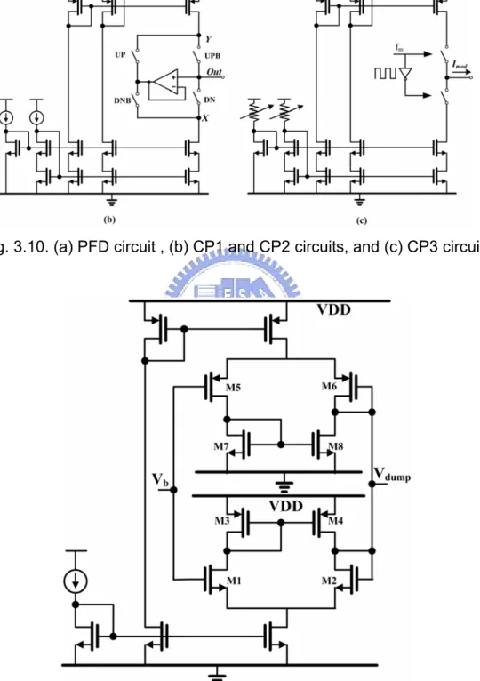
Fig. 3.10. (a) PFD circuit , (b) CP1 and CP2 circuits, and (c) CP3 circuit...43
Fig. 3.11. Unity gain buffer circuit used in dual-path loop filter. ...43
Fig. 3.12. Die photograph of the proposed SSCG...45
Fig. 3.13. Measured VCO frequency tuning curve...45
Fig. 3.14. Measured jitter of SSCG output at 400MHz when (a) SSC off (b) SSC on of 1.5% spread ratio...46
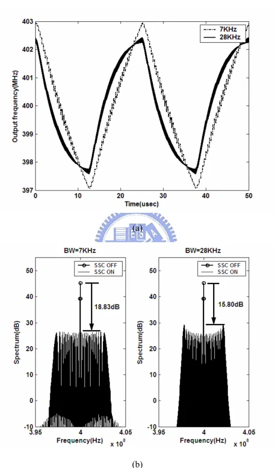
Fig. 3.15. Measured spectra of the 400 MHz output signal (a) without modulation, (b) with 1.5% center-spread and 7 kHz bandwidth, and (c) with center-spread 1.5% and 28 kHz bandwidth...47
Fig. 4.1. Block Diagram of two-point modulation PLL. ...52
Fig. 4.2. Linear model of TP-SSCG. ...52
Fig. 4.3. Phase noise simulation for different PLL loop bandwidths...55
Fig. 4.4. SSCG behavior model in MATLAB...58
Fig. 4.5. Frequency swings for OP-SSCG and TP-SSCG under different loop bandwidths with the ΔΣ modulator noise...59
Fig. 4.6. Spectra simulation results for OP-SSCG and TP-SSCG under different loop bandwidths with the ΔΣ modulator noise...59
with the ΔΣ modulator noise and the VCO noise (a) original (b) filtering out the VCO noise.
...61
Fig. 4.8. Spectra simulation results for OP-SSCG and TP-SSCG under different loop bandwidths with the ΔΣ modulator noise and the VCO noise. ...62
Fig. 4.9. Spectra simulation results for OP-SSCG and TP-SSCG under different loop bandwidths without any noise...62
Fig. 4.10. Simulation results for gain mismatch effects under different loop bandwidths. ...63
Fig. 4.11. The block diagram of proposed TP-SSCG...67
Fig. 4.12. (a) Proposed DAC (b) Timing diagram for the proposed DAC. ...67
Fig. 4.13. Extended range MASH 1-1 ΔΣ modulator. ...69
Fig. 4.14. (a) VCO circuit and (b) delay cell used in VCO. ...69
Fig. 4.15. TP-SSCG die photograph. ...69
Fig. 4.16. Measured spectra of 400 MHz output frequency (a) at non-spread spectrum mode, (b) of conventional SSCG with 2.5% spread ratio, and (c) of TP-SSCG with 2.5% spread ratio. ...71
Fig. 4.17. Measured jitter of 400MHz output frequency (a) at non-spread spectrum mode, and (b) of TP-SSCG with 2.5% spread ratio. ...72
Fig. 5.1. The block diagram of the proposed TPDL-SSCG...77
Fig. 5.2. (a) Proposed DAC. (b)Timing diagram for the proposed DAC. ...77
Fig. 5.3. Simplified block diagram of the dual path loop filter...79
Fig. 5.4. Linear model of the proposed TPDL-SSCG. ...79
Fig. 5.5 Simulation results of frequency error with a frequency sweep input ...82
Fig. 5.6 Phase noise simulation for FN-SSCG and TPDL-SSCG ...82
Fig. 5.7. Simulation results for the FN-SSCG and the TPDL-SSCG under different loop bandwidths. ...86
Fig. 5.8 .Spectrum simulation results with the ΔΣ modulator noise for the FN-SSCG and the PDL-SSCG under different loop bandwidths. ...87
Fig. 5.9. Spectrum simulation results without the ΔΣ modulator noise for the FN-SSCG and the TPDL-SSCG under different loop bandwidths. ...87
Fig. 5.10. Simulation results for gain mismatch impact on spread ratio for the TPDL-SSCG.89
Fig. 5.11. Block diagram of the proposed profile generator and ΔΣ modulator. ...92
Fig. 5.12. VCO circuits. ...92
Fig. 5.13. Die photograph of the proposed TPDL-SSCG. ...94
Fig. 5.14. Measured spectra (a) at non-spread spectrum mode, (b) of the conventional FN-SSCG, and (c) of the proposed TPDL-SSCG...95
Measurement condition: RBW= 100 kHz, VBW= 100 kHz and Peak-Hold mode...95
Fig. 5.15. Measured spectra for the TPDL-SSCG (a) with SSC-off (b) with SSC-on ...96
Measurement condition: RBW=10 kHz, VBW= 10 kHz and Peak-Hold mode...96
Fig. 5.16. Measured modulation profile in time domain. ...97
Fig. 5.17. Measured jitter for the TPDL-SSCG (a) with SSC-off, (b) with SSC-on. ...97
Fig. A.1. VCO model with jitter built in Matlab...110
CHAPTER 1
Introduction
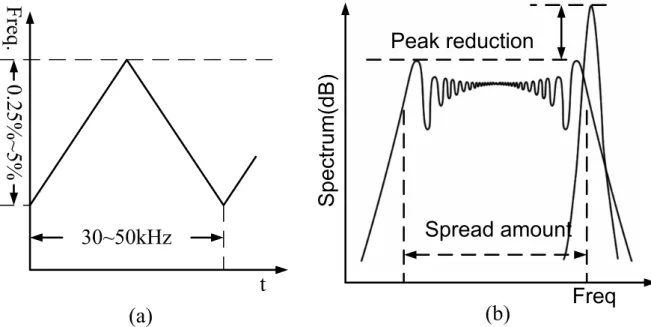
With the progress of CMOS technology, the operated frequency of electrical devices has been increased to meet the demand of high performance. When the operation frequency of electrical equipments is increasing rapidly, it radiates or generates more electromagnetic interference (EMI). Excessive EMI has disastrous damage to communication system; therefore, EMI levels have been strictly defined for different devices and systems. There are kinds of EMI standards defined by Federal Communication Commission (FCC) in USA or CISPR which is a committee of the International Electrotechnical Commission (IEC). For example, in the PC-based equipments, the frequency of microprocessor is up to several GHz and its EMI emission may exceed the related standard. The same case happens in portable devices with high speed data throughput like serial advanced technology attachment (SATA). Therefore, an effective and low cost method to reduce EMI is necessary. Several techniques have been used to diminish EMI, such as shielding [1], slew-rate limitation [1], filtering [1], and spread-spectrum clocking (SSC) [2]. Among these techniques, SSC, a technique of reducing the clock power of fundamental frequency as well as its harmonics, has been proven to being the most suitable and cost effective way to alleviate EMI [2] for clock-based systems. It also offers a good way to be integrated in VLSI chips. The function of SSC is shown in Fig. 1.1(a) and (b). When a clock generator turns on the mechanism of spread-spectrum clocking, the output of the clock generator is not a constant frequency; instead, it is a variable frequency with a fixed and slow modulation profile as shown in Fig. 1.1(a). From the view point of communication, it acts like a frequency modulator with a dedicated modulation profile. The modulation profile illustrated here is a triangular wave with two important parameters: spread ratio and modulation frequency. Usually, a peak-to-peak spread ratio within 0.25% to 5% and a modulation frequency within 30 kHz to 50 kHz are usually used. The spectra of the output when SSC is off and on are shown in Fig. 1.1(b). The spectrum has a peak reduction with a specified spread amount when SSC is on; therefore, the spread-spectrum clocking can effectively reduce the EMI levels.
30~50kHz
0.25%~5%
t
Fr
eq
.
Peak reduction
Spread amount
Freq
Spectrum(dB)
(a)
(b)
Fig. 1.1. Illustration of spread-spectrum clocking: (a) frequency output with time (b) spectra output when SSC off and on.
1.1 Review of SSCG
Spread-spectrum clock generator (SSCG) is the clock generator utilizing the technique of SSC. Phase locked-loop (PLL) is a popular candidate for a clock generator in VLSI technology. Therefore, PLL becomes an important employee for SSCG. The block diagram of PLL with various modulations is shown in Fig. 1.2. The key components of the PLL are a phase frequency defector (PFD), a charge-pump (CP) current, a loop filter (LF), a voltage-controlled oscillator (VCO) and a programmable counter (PGC). There are three major SSC techniques employed in PLL. First, modulating the divider using a ΔΣ modulator [8] in a PLL like (A) or (D) in Fig. 1.2. It is called the Fractional-N based SSCG. The second type is to modulate the VCO directly like (B) in Fig. 1.2. Last, one may combine the multiphase outputs with special phase interpolation algorithms to achieve SSC function like (C) in Fig. 1.2. Here, three major techniques are reviewed.
1.1.1 Fractional-N based SSCG
The block diagram of a fractional-N based SSCG [8] is shown in Fig. 1.3. It is basically a fractional-N PLL using a ΔΣ modulator to modulate the divider. An up-down counter is used to generate a triangular modulation profile. The k-bits outputs of the counter are fed into the first-order ΔΣ modulator to control the dual modulus divider N-1/N+1. As a result, the output of the PLL can also track the triangular modulation profile and establish the function of spread-spectrum clocking. The first-order delta modulator is simply a (k+1) bits accumulator. The modulation frequency is determined by bit number and operation frequency of the up-down counter while the spread ratio is determined by bit number of the up-down counter and bit number of the accumulator. In this thesis, k=4 means that the bit number of the up-down counter is 4 and the bit number of the accumulator is 5. N=402. Therefore, the spread ratio is ±1/402=±0.124%. Besides, the reference frequency Fref=27 MHz and M=81.
The modulation frequency can be evaluated by 27 MHz/81/32=10.417 kHz. The advantage of this technique is that the spread ratio and modulation frequency can be easily adjusted by change the parameters of the up-down counter, composed of some simple digital circuits.
PFD
Filter
VCO
Fref
Fvco
1/M
N-1/N+1
U/D
K bits
1 bit
ΣΔ modulator
Fig. 1.3. Block diagram of Fractional-N based SSCG.
Therefore, it can be integrated in the VLSI chips with few costs. However, the quantization noise of the sigma-delta modulator will degrade the jitter performance and EMI performance and needs carefully design.
1.1.2 SSCG Using Direct VCO Modulation
The block diagram of the SSCG using direct VCO modulation [3] is shown in Fig. 1.4. It utilizes an extra charge-pump Ip2 combined the special loop filter components R1, R2, C1
and C2 to generate the triangular waveform as the modulation profile. When R1C1=R2C2, the
relationship between VCO controlled voltage Vcntl and Ip2 can be found as
2 1 2 1 cntl p V I = sC C . (1.1)
Therefore, the triangular waveform can be formed when Ip2 is a rectangular waveform.
In order to pass the modulation profile, the loop bandwidth of the PLL needs to be much smaller than the frequency of the triangular waveform. The advantage of this technique is that the architecture is very simple; however, the capacitors in the loop filter is so large (C1=0.33
uF and C2=0.22 uF) that makes it is hard to be integrated in the chips. Moreover, the spread
ratio is related to the process parameters and the accuracy is also a concern.
1.1.3 SSCG Using a Multiphase VCO
The block diagram of the SSCG using a multiphase VCO with a spread spectrum generator is shown in Fig. 1.5 [7]. The VCO has 32 phase outputs. The spread spectrum generator picks up a sequence of suitable phases to periodically change the period of the VCO. The simplified block diagram of the spread spectrum generator is shown in the down side of Fig. 1.5. The spread spectrum generator uses a controller to adjust the up-down counter dependent on the current output phase. The up-down counter is fed into a 5-to-32 decoder to pick up one of 32 phases via 32-to-1 multiplexer and then feedback to the up-down counter with a frequency divided by 2. The advantage of this technique is that only some digital circuits are added to implement the function of SSCG and therefore, it is easy to be integrated in VLSI. But the maximal jitter is determined by the resolution of the multiphase generation. If one needs to minimize the jitter, the number of VCO phase needs to
Phase detector Filter Multiphase VCO Fref Fvco /M 32 phase Spread spectrum generator /2 output UP/DN counter 5 to 32 decoder controller Dual 32-1 mux 10 bits 64 bits
32 clocks from VCO
Buffer /2
Fig. 1.5. Block diagram of SSCG using the multiphase VCO.
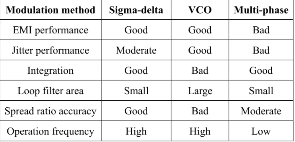
Table 1.1 SSCG Performance Comparisons for Different Architectures Modulation method Sigma-delta VCO Multi-phase
EMI performance Good Good Bad Jitter performance Moderate Good Bad
Integration Good Bad Good Loop filter area Small Large Small
Spread ratio accuracy Good Bad Moderate Operation frequency High High Low
be increased and in the mean time, the power consumption and area will be increased as well. In other words, it is not suitable for high frequency application like SATA. In addition, the accuracy of each phase will affect the linearity of the modulation profile and the EMI performance.
1.1.4 Performance Comparison Between Different SSCG Architectures
The SSCG performance comparisons for different architectures are listed in Table 1.1. Three architectures discussed above (1.1.1~1.1.3) are taken into consideration. Key parameters like EMI performance, jitter performance, flexibility to integration, loop filter area, spread ratio accuracy and operation frequency are compared. The Fractional-N based SSCG using a sigma-delta modulator has the most advantages among these architectures; therefore, there are more and more literatures [9], [10], [13], [15], [22], [23], [24], [36], [37] using this architectures. The SSCG using direct VCO modulation has advantages of good EMI and jitter performance and high operation frequency except some drawbacks like large loop filter areas, obstacles to triangular waveform generation and bad spread ratio accuracy.
1.2 Motivation
SSCG is known to a key component in many consumer and portable products such as personal computer, notebook computer, printer, projector, scanner and LCD TV. The request of a low cost and high performance SSCG is expanding especially for integration on system on chips (SOC). In this thesis, we proposed four different SSCGs with three kinds of modulation schemes. First, the fractional-N PLL with a ΔΣ modulator [8]-[9] has advantages of being fully digital controlled and of being indirect modulated the sensitive VCO according to the analysis in section 1.1. But, the input range of the conventional ΔΣ modulator is limited. The required input range is determined by the spread ratio and target frequency. An overflow problem which may be encountered as the spread ratio is exceeded its input range. This problem will result in the stability problem and frequency error; therefore, the EMI reduction and jitter performance will be degraded very much. In Chapter 2, the input range of the proposed ∆Σ modulator is enhanced to accommodate a wide variety of divider ratio. In Ref.
[9], a method with a level shifter is used to shift the modulation profile to keep within the input range of the ∆Σ modulator. However, some more circuits and complicated algorithm are needed. Here, a simpler method with an extra bit added to the output of the first stage modulator is presented to extend the input range of ∆Σ modulator, solve saturation problem and thus, reduce the jitter introduced by the non-correct modulation.
Then, a voltage controlled oscillator (VCO) modulated SSCG has the advantages of a simple circuit structure and the absence of sigma-delta modulator noise, but has two major issues according to the analysis in section 1.1. One major issue is that the generation of the triangular waveform depends on special relationship between loop filter. This dependency makes it less flexible. The other issue is the required large capacitance (more than tens of nF) to make it hard totally integration the loop bandwidth of a PLL has to be much less than the modulation frequency to allow the frequency variation of the VCO. Recently, the technique of capacitance multiplication is proposed to eradiate this problem [16], [18]-[20]. However, in order to accommodate another charge pump to generate the triangular modulation, a floating capacitor is connected [16]. The floating capacitor needs extra masks and process steps. In Chapter 3, a modified architecture with a grounded capacitor in mixed configuration containing both a dual-path loop filter (DPLF) [18] and an extra charge-pump circuit is proposed to attain a smaller size and triangular modulation. This method also reduces both hardware complexity and chip area.
Finally, re-considering the fractional-N based SSCG with a ΔΣ modulator, the allocation of three frequencies of modulation, loop bandwidth, and phase comparison are very decisive for the performance of low jitter and good EMI. The loop bandwidth needs to be large enough to react sufficiently to the triangular waveform. Otherwise, the modulation profile is distorted and EMI suppression is compromised [24]-[26]. In contrast, much less than the comparison frequency is normally required to filter the quantization noise of ΔΣ modulator and to obtain low jitter. To obtain sufficient suppression in the case of a large bandwidth, a third-order ΔΣ modulator is normally employed. However, the power consumption and area associated with this type of modulator are a disadvantage. Therefore, in Chapter 4 and 5, an alternative method with two-point modulation is proposed. Both the divider ratio and the voltage controlled oscillator are varied. An all-pass characteristic of the two point modulation
performance caused by the ΔΣ modulator can be improved at the same time. Furthermore, only a second order ΔΣ modulator is required, which reduces both the required power and chip area. The simulation time is also a concern when implementing SSCGs due to low modulation frequency and high output frequency. In order to obtain the correct EMI levels, the output spectrum obtained through Fourier transform needs large data and therefore requires the long simulation time. Here, an efficient model built in Matlab [33] is developed to reduce the simulation time dramatically.
1.3 Organization
In the rest of this dissertation, we focus on the design and implementation of the SSCG based on PLL. Three proposed SSCG are discussed.
In chapter 2, an extended input range ΔΣ modulator is developed and a fractional-N based SSCG utilizing the new ΔΣ modulator is designed and analyzed. Theoretical analysis for the input range of the new ΔΣ modulator is derived. Few simulations are made to compare the proposed SSCG and the conventional SSCG. Experimental results are coincided with the simulation results.
Chapter 3 focuses on the improvement of the SSCG using direct VCO modulation. A compact SSCG using a dual-path loop-filter combined another charge-pump can make the SSCG fully integration. The non-ideality of the dual-path loop-filter is analyzed. The phase noise of the SSCG is intensively studied. The modulation limitation and spurious modulation is also analyzed. Measurements show good agreement with the simulation results.
Chapter 4 presents a proposed SSCG with a two-point modulation. By mixing the analog modulation (VCO modulation) and the digital modulation (ΔΣ modulation), the proposed SSCG features good EMI performance and jitter performance by optimizing the loop bandwidth and the order of the ΔΣ modulator. The jitter and EMI from the quantization noise of the ΔΣ modulator and the VCO phase noise are deeply diagnosed. The simulation time is dramatically reduced by a well-built Matlab model. This model can analyze and predict the EMI performance and the jitter performance. The proposed DAC and other circuits are described. Measurements show good correspondence with the simulation results.
Chapter 5 develops another two-point SSCG for the application of SATA. The proposed DAC and the adopted dual-path loop filter are discussed. The linear model of the system including phase noise and jitter are presented. The major circuits are also discussed. Measurements can meet SATA specifications and agree with the simulation results.
CHAPTER 2
A Wide Input-Range ΔΣ Modulator for
Applications to Spread-Spectrum Clock
Generator
A spread-spectrum clock generator (SSCG) using fractional-N phase-locked loop (PLL) with an extended range sigma-delta (ΔΣ) modulator is presented. The proposed ΔΣ modulator simply adds an extra output bit in the first stage modulator. It can enlarge the input range about three times as compared to the conventional modulator and solve the saturation problem when the input exceeds the boundary of the conventional modulator. A flexible digital modulation controller can generate center and down spread-spectrum modulation and each has spread ratios of 0.4%, 0.8%, 1.6% and 3.2%. The proposed SSCG has been fabricated in TSMC 0.35-um double-poly quadruple-metal CMOS process with output frequency of 300 MHz. The active area is 0.63×0.62 mm2 and the power consumption is 17.5 mW.
2.1 Introduction
Spread-spectrum clock generators have been widely used in the PC-based equipments as an effective method to reduce the high frequency emissions. Through the frequency modulation, the energy in each clock harmonic is spread evenly over a dedicated bandwidth, and thus, the power level at each clock harmonic is reduced as much as 10-20 dB, depending on the modulation index and the speed. Several techniques for spectrum spreading have been developed [2]-[9]. The fractional-N PLL with a ΔΣ modulator [8]-[9] has recently received much attention due to its advantages of being fully digital controlled and of being indirect modulated the sensitive VCO. The wider input range of the ΔΣ modulator is requested under the spread spectrum mode because the divider ratio changes all the time. An overflow problem may be encountered as the divider is set near the input boundary. Especially, in PC applications, a wide variety of divider numbers are often applied for different CPU
frequencies. For an example with the reference frequency (Fref) at 14.318 MHz and the output
frequency at 300 MHz, the average value of the divider is 20.9526. Under a 3.2% deviation in center spread-spectrum mode, the variation of the fractional part is from 0.6173 to 1.2878, which crosses the unity boundary. However, the input range of the conventional ΔΣ modulator is limited under unity as its architecture is defined. Exceeding the input range will cause the stability problem and frequency error. In this study, the input range is enhanced to accommodate a wide variety of divider ratio. In Ref. [9], a method with a level shifter is used to shift the modulation profile to keep within the input range of the ∆Σ modulator. Therefore, some extra circuits are needed and make the modulator more complicated. Here, a simpler method with an extra bit added to the output of the first stage modulator is presented to extend the input range of ∆Σ modulator, solve saturation problem and thus, reduce the jitter introduced by the non-correct modulation.
2.2 Proposed Spread-Spectrum Clock Generator
The block diagram of the proposed spread-spectrum clock generator is shown in Fig. 2.1. It is composed of a phase frequency detector (PFD), a charge pump circuit (CP), an off-chip loop filter (LF), a VCO, an asynchronous programmable counter (ASPC) and a digital modulation controller (DMC). The ΔΣ modulator of MASH type is employed due to the advantages of unconditional stability and easy high-order implementation. [11], [12]
2.2.1 Digital Modulation Controller
DMC which consists of a spread-spectrum profile generator and a ΔΣ modulator is used to control the divider value of ASPC. The profile generator as shown in Fig. 2.2(a) consists of a triangle wave generator and a profile controller to control the frequency deviation and spreading direction. The output of the controller denoted as INSD[k], where k is an integer, is fed to the ΔΣ modulator. The waveform of INSD[k] is shown in Fig. 2.2(b). The amplitude of the triangle wave, Vamp, controlled by SSPER is used to decide the frequency deviation ratio.
The mean value of the triangle wave, FNmean, controlled by SSTYP, is used to decide the
center frequency of the SSCG. The maximal number of INSD[k], INSD[k]max, is given as max
[ ] mean amp
PFD (external)LF VCO ASPC Fref Vcntl Fvco Spread spectrum profile generator Delta-sigma modulator INSD CP INTN 6N
Digital modulation controller
Fig. 2.1. Block diagram of the spread-spectrum clock generator.
SSTYP SSPER
Spread-spectrum profile generator
INSD[k]
Triangle wave
Profile controller
(a)
(b)
Fig. 2.2. (a) Proposed spread-spectrum profile generator, and (b) The output waveform at INSD.
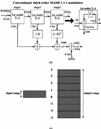
Fig. 2.3. Convectional third-order MASH 1-1-1 modulator (a) architecture and (b) input and output range.
Fig. 2.4. Proposed extended range MASH-type modulator (a) architecture and (b) input and output range.
The peak-to-peak frequency deviation ratio, Fdev,pp, is given as , 2 2 amp dev pp BT mean V F INTN FN × = × + , (2.2)
where INTN is the integer part of the divider and BT is bit width of the modulator. In this design, there are two kinds of spread direction, i.e. center spread and down spread, and four peak-to-peak frequency deviation indexes: 0.4%, 0.8%, 1.6% and 3.2%. The frequency of the triangle wave is set at 40 kHz.
2.2.2 Modified ΔΣ Modulator
For clarity, the disadvantage of the conventional modulator as shown in Fig. 2.3(a) is indicated. Three first-order modulators are cascaded to implement a third-order MASH 1-1-1 modulator. The block diagram of each stage is shown in the right of Fig. 2.3(a), which is simply an accumulator with one-bit carry output. Both the input and output ranges are illustrated in Fig. 2.3(b). The exact input range is from1/2BT to(2BT −1)/2BT. It implies
INSD[k]max is (2BT-1). Here BT=10. Each of the outputs of the three stages is 0 and 1. The
output of the second stage passes through a differentiator and then its possible values become -1, 0 and 1. The output of the third stage passes through two differentiators and then its possible values become -2, -1, 0, 1 and 2. Summing the three branches together yields 8 possible outputs, i.e., -3, -2, -1, 0, 1, 2, 3 and 4. Therefore, the output range of the modulator is from -3 to +4 to accommodate all the possible inputs. So that 3bits at output are built. If INSD[k] is modulated beyond (2BT-1), then the modulator is saturated and can not function well. Therefore, such an arrangement can’t meet our requirement.
The proposed one with extended input range is shown in Fig. 2.4(a). Two different kinds of first-order ΔΣ modulator are employed. The block diagrams are shown in the bottom of Fig. 2.4(a). In stage-1 modulator, a 2-bit carry output denoted as C0[k] is designed. Stage2 and stage3 are unchanged. The inputs to the stage-1, stage-2, and stage-3 are denoted as INSD[k], EN1[k], and EN2[k], respectively. With the 2-bit carry output in stage-1 modulator, the input value INSD[k] can be set equal to or larger than one without error occurrence. As the input value is bigger than one, the stage-1 modulator can response quickly the integer part of the input to the output and will not saturate the following stages. The difference equation for
stage-1 modulator is given as follows. Let ] 1 [ 1 ] [ ] [k =INSD k +EN k− SUM . (2.3) Then ( 1) ( 1) ( 1) ( 2) 1[ ] [ ], 0 [ ] 2 [ ] 2 , 2 [ ] 2 [ ] 2 , 2 [ ] 3 2 [ ] 3 2 , 3 2 [ ] 2 BT BT BT BT BT BT BT BT BT BT EN k
SUM k for SUM k
SUM k for SUM k
SUM k for SUM k
SUM k for SUM k
+ + + + = < < = − ≤ < = − ≤ < × = − × × ≤ < . (2.4) And ( 1) ( 1) ( 2) 0[ ] 0, 0 [ ] 2 1, 2 [ ] 2 2, 2 [ ] 3 2 3, 3 2 [ ] 2 BT BT BT BT BT BT BT C k for SUM k for SUM k for SUM k for SUM k + + + = < < = ≤ < = ≤ < × = × ≤ < . (2.5)
From (2.4), the maximal number of EN1[k], EN1[k]max can be found as 2BT-1. From
(2.5), the maximal number of C0[k] is equal to 3 and, thus, a two-bit carry output is needed. From (2.4) and (2.5), the maximal number of SUM[k], SUM[k]max can be found as 2(BT+2)-1.
Substitute EN1[k]max and SUM[k]max into (2.3), INSD[k]max can be obtained as 3×2BT −1.
The maximal input number of the proposed modulator is about 3 times compared to conventional modulator and hence extra two input bits are added. The output range of the proposed modulator becomes from -3 to 6. One extra bit is added. The input range and output range of the proposed modulator are shown in Fig. 2.4(b). The minimal input number of the proposed modulator is 1, which is the same to the conventional one.
From (2.1), one can get the following equation.
max
[ ] 3 2BT 1
mean amp
INSD k = FN +V = × − (2.6)
From (2.6) the advantages of the proposed modulator can be seen. When FNmean is equal
to (2BT-1), which is the largest input number for the conventional modulator, the maximal number of Vamp is 0. Here, the maximal number of Vamp for the proposed architecture can be
found as (2BT-2) by (2.6). When FNmean is equal to 1, which is the smallest input number for
the conventional modulator, the maximal number of Vamp is 0. However, in proposed architecture, we can reduce the integer part of the divider by 1, and change the FNmean to
Fig. 2.5. The 300MHz output frequency simulation results for conventional (solid line) and proposed (broken line) architectures at the 3.2% center-spread spectrum mode.
(a) (b)
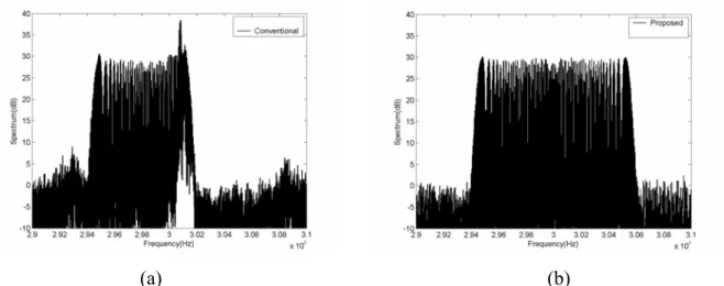
Fig. 2.6. The 300MHz output FFT simulation results of (a) conventional architecture and (b) proposed architecture at the 3.2% center-spread spectrum mode.
Delay#2 Delay#3 Delay#1 Mn1 Mn2 Mp1 Mp2 In+ In- Out-Out+ Vcntl Mn3 Mn4
(a) VCO
(b) delay cell
Fig. 2.7. (a) VCO with three-stage delay cells and (b) Schematic of each delay cell.
R1 C1 C2 R3 C3 BIAS CIRCUIT BIAS CIRCUIT Vcntl UP DN 2.5V Loop filter
(2BT+1). Then the maximal number of Vamp is 2BT. The maximal frequency deviation appears when FNmean=Vamp, which is almost half of the input range. Therefore, one can
efficiently use the the proposed modulator by simply shifting FNmean to FNmean +2BT.
The numerical comparisons of the output frequency between two architectures are illustrated in Fig. 2.5 and Fig. 2.6. The results are obtained from time-domain model built by MATLAB. The simulation case is a 300 MHz output with a 3.2% center-spread spectrum with the input frequency of 14.318 MHz. The fractional part of the modulator is changed between 0.6173 and 1.2878 and the mean value is 0.9526 as we mentioned above. Given BT=10, FNmean = 2BT×0.9526 = 975, and Vamp =2BT×(1.2878-0.6173)/2 = 343.
Fig. 2.5 shows the output frequency swing with respect to time for two architectures. It is shown that the solid line from the conventional modulator is clamped near 301 MHz, On the contrary, the curve by broken line can response well. Fig. 2.6(a) and 2.6(b) show the corresponding FFT results. The output spectrum in Fig. 2.6(a) for conventional modulator appears a peak near center frequency and a narrow peak-to-peak spreading ratio. However, the proposed one can correctly response the spreading profile.
The maximal frequency deviation can also be predicted. In above case, the maximal number of Vamp can be found as 974, which is equal to (FNmean-1). The INTN in this case is
20. From (2.2), the maximal peak-to-peak frequency deviation ratio can be found as 9.07%. On the contrary, the conventional one only achieves 0.23% maximal peak-to-peak frequency deviation ratio. In summary, using this simple two carry-bits technique, the modulator can avoid the saturation region and enlarge the frequency deviation. Usually the spread spectrum ratio is less than 5% because of the jitter consideration. Therefore, the proposed SSCG can fulfill the requirement.
2.3 Circuit Description
The circuits in building blocks of Fig. 2.1 are briefly described. The wide band VCO which consists of the three stages of differential delay cells is shown in Fig. 2.7(a). The schematic of the cell is shown in Fig. 2.7(b). [10] The cross-coupled transistors, Mn1 and Mn2, give the VCO full swing and sharpen the edge of the output signal to reduce the jitter.
The transistors, Mn3 and Mn4, control the frequency of VCO. The voltage to current converter that will cause extra jitter is not needed because it is a voltage-controlled oscillator. The tail current source is also avoided for low voltage application and for lower flicker noise up-conversion. [10] A 6-bit ASPC is adopted here for low power consumption. The charge-pump circuit and loop filter circuit are shown in Fig. 2.8. The cascoded current source is employed for good immunity against the power supper noise. The wide-swing bias circuit, which is not shown in the Fig. 2.8, is designed for low voltage operation. The controlling signals for UP and DN switches are fed from the output of PFD. The current of the charge pump is 6 uA and an external 3rd-order low-pass filter is used in this work to filter out the quantization noise of the modulator. The loop bandwidth of the PLL is traded off between modulation speed and modulator quantization noise. Here, the loop bandwidth of 150 kHz is chosen. The values of the components are listed in Table 2.1.
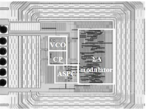
2.4 Measurement Results
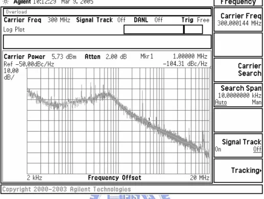
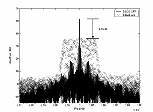
The proposed SSCG has been fabricated in TSMC 0.35-μm double-poly quadruple-metal CMOS process. Fig. 2.9 shows the microphotograph of the chip. The active area is 0.63×0.62 mm2 and the total area including pads is 1.36×1.35 mm2. The tuning sensitivity of VCO is shown in Fig. 2.10 with a gain of 270 MHz/V near 300 MHz output. The VCO reveals a good linear voltage to frequency transfer curve and has a maximal frequency more than 600 MHz. Fig. 2.11 indicates that the proposed SSCG operating at nonspread-spectrum mode achieves -104.31 dBc/Hz at 1 MHz offset from the carrier. It also reveals the closed-loop bandwidth of about 150 kHz. Fig. 2.12(a) shows the measured output spectrum at nonspread-spectrum mode. The amplitude is about 5.74 dBm. Fig. 2.12(b) shows the measured output spectrum under the 0.8% option in center spread-spectrum mode. The peak reduction is about 15.82 dB as compared to Fig. 2.12(a), which is very close to predicted results of 15.68 dB shown in Fig. 13. Fig. 2.12(c) shows the measured output spectrum under the 3.2% option in center spread-spectrum mode. The peak reduction is about 20.54 dB as compared to Fig. 2.12(a) that is slightly smaller than the predicted 21.36 dB in Fig. 2.14. This is because there exists small peaks at two ends of the measured spectrum. The phenomenon is due to the insufficient loop bandwidth. When the loop bandwidth is not
Fig. 2.9. Microphotograph of the proposed SSCG. Kvco=270MHz/V @ 300MHz 100 150 200 250 300 350 400 450 500 550 600 650 0.5 0.7 0.9 1.1 1.3 1.5 1.7 1.9 2.1 2.3 2.5 Vcntl(V) Frequency(MHz)
Fig. 2.11. Phase noise measurement at non-spread spectrum mode.
(b)
(c)
Fig. 2.12. Measured spectrum (a) at non-spread spectrum mode, (b) at spread-spectrum mode with 0.8% center spread ratio, and (c) with 3.2% center
Fig. 2.13. Comparison for FFT simulation results for spread-spectrum mode on with 0.8% center spread (o) and off (black).
Fig. 2.14. FFT simulation results for spread-spectrum on with 3.2% center spread (o) and off (black).
(a)
(b)
Fig. 2.15. Measured period jitter (a) at non-spread spectrum mode, and (b) with the center spread ratio of 0.8%.
enough to pass through high frequency components of the triangle signal, the modulation profile will be destroyed especially at the two ends. It is also founded in our simulation result of Fig. 2.6(b). The jitter performances at non-spread spectrum mode and spread-spectrum mode are shown in Fig. 2.15(a) and 2.15(b), respectively. The peak-to-peak jitter is 110 ps in non-spread spectrum mode and 140 ps under the 0.8% option. Table 2.1 gives the performance summary of the SSCG. Table 2.2 gives the comparison of EMI reduction between simulation and measurement.
2.5 Summary
In this work, an extended range MASH-type ΔΣ modulator is presented to solve the input range problems when the fractional-N PLL is operated as the SSCG. At the expanse of two extra input bits and one extra carry bit the proposed modulator is proven to have about 3 times input range as compared to conventional modulator. In the meantime the modulator can handle up to 9% frequency deviation. The spreading ratio and direction can be easily obtained by adjusting the amplitude and DC value of the digital triangle wave. The SSCG is implemented in TSMC 0.35 μm double-poly quadruple- metal CMOS process. Measurement results at 300 MHz under 0.8% and 3.2% spread ratio are in good agreements with the predictions. These results can be further applied to a wide variety of clock sources with spreading spectrum.
Table 2.1 Performance Summary
Modulation Method Modulation on divider Modulation Type Center-spread/Down-spread Modulation Frequency 40 kHz Spread Ratios(pp) 0.4%,0.8%,1.6%,3.2% Output Frequency 300 MHz Input Frequency 14.31818 MHz VCO Gain(Kvco) 270 MHz/V Loop bandwidth ~150 kHz Loop filter R1=12 kΩ C1=400 pF C2=40 pF R3=10 kΩ C3=10 pF EMI reduction 15.82 dB @ 0.8% center spread ratio
20.54 dB @ 3.2% center spread ratio Jitter(PP) 110 ps at non-spread spectrum mode Jitter(PP) 140 ps at spread spectrum mode (0.8%) Chip Area (active) 0.63×0.62 mm2
Power Dissipation 17.5 mW including output buffer @ 2.5V
Table 2.2 EMI reduction Between Simulation and Measurement Condition Simulation results Measurement results Center-spread 0.8% 15.68 dB 15.82 dB Center-spread 3.2% 21.36 dB 20.54 dB
CHAPTER 3
A Fully Integrated Spread Spectrum Clock
Generator by Using Direct VCO Modulation
A compact architecture for a fully-integrated spread spectrum clock generator (SSCG) using VCO direct modulation is presented in this thesis. A dual-path loop filter in the phase-locked loop (PLL) is employed to reduce the size of the capacitance in the filter with the aid of an extra charge pump and a unity gain amplifier. At the same time, a third -charge pump which generates triangular waves is used to perform the function of a spread-spectrum. The proposed circuit has been fabricated using a 0.35 μm CMOS single-poly quadruple-metal process. The clock rate from 50 to 480 MHz with a center spread range of between 0.5% and 2% are verified and are close to the theoretical analyses. The size of the chip area is 0.82×0.8 mm2 (including the loop filter) and the power consumption was 27.5 mW at 400 MHz.
3.1 Introduction
The electromagnetic interference (EMI) in electronic devices such as a PC, printer, PCI Express and SATA increases rapidly as the clock speed is raised. In many applications, clock generators are one of the major contributors of EMI. Spread-spectrum clock generators (SSCG) are proven to be an efficient way to reduce EMI levels [2]-[4], [7]-[9], [13]-[15]. A SSCG is basically a PLL with an appropriate frequency-modulated output. The frequency modulation is used to spread the output spectrum. There are three kinds of modulation schemes employed in PLLs. The first type involves a change to the divider made by a sigma-delta modulator [8]-[9]. The second type includes either digital manipulation of the output of a multiphase PLL or the use of a DLL/phase interpolator combo on the output of a standard PLL [5]-[7]. The last type involves direct modulation of the VCO in PLL [3]-[4], [16]-[17]. The latter has the advantages of a simple circuit structure and the absence of sigma-delta modulator noise. But the loop bandwidth of a PLL has to be much less than the modulation frequency to allow the frequency variation of the VCO. In general, the required loop bandwidth is about one of ten times that in the modulation. The modulation frequency is
Fig. 3.1. Proposed SSCG.
typically around 30 kHz to 50 kHz so that the loop bandwidth is around 3 kHz to 5 kHz. This leads to a large capacitor of more than 10nF in the loop filter, which becomes too large to be integrated in the chip [3].
Recently, the technique of capacitance multiplication is proposed to eradiate this problem [16], [18]-[20]. However, in order to accommodate another charge pump to generate the triangular modulation, a floating capacitor is connected [16]. The floating capacitor in a standard CMOS process can be PIP (poly to poly) or MIM (metal to metal) and needs extra masks and process steps. It also has the area and cost penalties comparable to those of a MOS capacitor. In this thesis, a modified architecture with a grounded capacitor in mixed configuration containing both a dual-path loop filter (DPLF) [18] and an extra charge-pump circuit is proposed to attain a smaller size and triangular modulation. This method also reduces both hardware complexity and chip area. Although, a non-linear modulation profile known as the ‘Hershey-Kiss’ profile [2] shows a better EMI performance, its nonlinear equations make it more expensive due to a larger area and power consumption. Therefore, the linear triangular profile is adopted in this thesis.
3.2 Proposed SSCG and its Theoretical Analysis
3.2.1 Proposed SSCG
The proposed SSCG is shown in Fig. 3.1. It consists of a phase-frequency detector (PFD), a dual-path loop filter [18] which is composed of two charge pumps CP1 and CP2, a
unity-gain buffer, two capacitors C1 and C2 and a resistor R1, a charge pump CP3,a VCO, and
a 8-bits programmable counter. The CP1 and CP2 provide the dual-path charging currents Ip1
and Ip2, respectively, to the loop capacitors. The CP3 provides the charging current Imod to the
grounded capacitor C1 in order to form the triangular waveform of the control voltage Vc. The
first path composed of the R1 and C2 is a low-pass filter. The second path composed of the C1
and unity gain buffer acts as an integrator. The voltages from these two paths are combined together so that a zero is created in transfer function. In order to obtain the multiplication effect of the capacitance C1, the pumping current Ip1 is set at Ip1=BIp2 with a factor B>>1. To
simplify the analysis, the higher order filtering effect of R3 and C3 is ignored in the following
given as
( )
1(
1)
1 1 1 2 1 1 c p R s R BC V F s I s sR C ⎛ ⎞ + ⎜ ⎟ ⎝ ⎠ = = + . (3.1)For a comparison, the conventional 2nd-order loop filter with only one charge pump Ip is
presented in Fig. 3.2(b), in which both the capacitor C1 and the unity gain buffer are replaced
by an equivalent capacitor C1T. The corresponding transfer function is given by
( )
1 1 1 1 2 1 2 1 1 1 2 1 1 T c p T T T T R s R C V F s I C C C C s sR C C C ⎛ ⎞ + ⎜ ⎟ ⎝ ⎠ = = ⎛ ⎞ + + ⎜ + ⎟ ⎝ ⎠ . (3.2)When compared with (3.1), it was found that two circuits have the same zero response under the condition of BC1=C1T. It implies that capacitance C1 in the former case is B times
smaller than C1T. The area of capacitor C1 can be reduced dramatically by using this
technique. In this work, B=50. Moreover, one of terminals in C1 is grounded. Therefore,
capacitor C1 can be realized by using the MOS capacitor. The pole in (2) is caused from R1
and a capacitor with C1T and C2 in series. If C1T>>C2. it is almost equal to that of R1C2 in
(3.1), It is generally the case that the pole is about ten to hundred times the zero, depending on the damping ratio of the system.
3.2.2 Analysis of the Non-ideality of the Dual-Path Loop Filter
The non-ideality of the dual-path loop filter can be viewed in two ways: filter transfer function and phase noise. The unity gain buffer is built by an OP-AMP, which can be modeled by the DC gain Av and the gain-bandwidth product ωt. The transfer function of unity
gain buffer can be expressed as
( )
( 1) 1 1 v v err t t A A A A s s s ω ω + = = + + , (3.3)Fig. 3.3. Block diagram with relevant noise sources.
By using (3.3) and re-calculating F(s), one can get
(
11 2)
1(
1 2)
1 ( ) 1 1 1 err t R A F s s sR C sBC sR C ω = + + + + . (3.4)Equation (3.4) can be reduced to
( )
1(
1 1)
1 2 1 err A R s R BC F s s sR C ⎛ ⎞ + ⎜ ⎟ ⎝ ⎠ ≈ + (3.5)when ωt >>1/(R1C2). When (3.5) is compared to (3.1), it can be expected that the gain error
will cause the ratio of capacitance multiplication to be higher than the expected.
With reference to phase noise analysis, the block diagram with relevant noise sources is shown in Fig. 3.3. Here, noise from CP1, CP2, the unity-gain buffer and VCO are considered
and denoted as 2 1 np I , Inp22, 2 nop
V , and Vnvco2 , respectively. The unity buffer is only modeled by
its gain error for the worst case scenario and the second order loop filter is adopted for the purpose of simplification. It should be noted that all noise sources are assumed to be white although this is only an approximate for VCO.
The noise spectral density at the PLL output SΦn(f) is represented as
( )
( )
( )
( )
2 2 2 2 2 21
n nvco np nop vco nvco cp np op nop
SΦ f =SΦ f +SΦ f +SΦ f = H V + H I + H V (3.6)
where SΦnvco(f), SΦnp(f), and SΦnop(f) are the noise spectral densities of VCO, both
charge-pump currents, and the unity gain buffer, respectively. The definition of 2
nvco
V can be found in [11]. From the PLL linear model shown in Fig. 3.3, the transfer functions are calculated as follows:
( )
( )
1 1 2 2 v cp d v NK F s H sN K F s K π π = + , (3.7)( )
1 2 2 2 1 v err op d v NK A H sN K F s K sR C π π = + + , (3.8)and
( )
2 2 v vco d v NK H sN K F s K π π = + . (3.9)Where Kv is the gain of the VCO in Hertz/Volts, Kd=Ip1/2π is the gain of the PFD and CP,
F(s) is the transfer function of loop filter of (3.5), and N is value of the divider. F1(s) is the
noise transfer function from CP1 and CP2 and can be found using
( )
1(
1)
1 1 1 2 1 err A R s R BC F s s sR C ⎛ ⎞ + ⎜ ⎟ ⎝ ⎠ = + . (3.10)From (3.10) it can be seen that the noise transfer function is slightly different to the signal transfer function (3.5). The capacitor multiplication factor in noise analysis is B not B. In addition, by comparing (3.8) and (3.9), the noise from the unity gain buffer and from the VCO have the same contribution when frequency is below 1/R1C2. The PLL phase noise
simulation results are shown in Fig. 3.4, where the solid line uses the traditional loop filter presented in Fig. 3.2(b). The solid line with a cross mark denoted by DPLF case1 uses the dual-path loop filter seen in Fig. 3.2(a) with 2 2
nop nvco
V =V . Finally, the dashed line with a circle mark denote by DPLF case 2 uses the dual-path loop filter shown in Fig. 3.2(a) with
2 0.1 2
nop nvco
V = ×V . Here, the VCO phase noise is assumed to be -100dBc at 1MHz offset frequency. From Fig. 3.4, it can be seen that the phase noise of solid line, solid line with a cross mark and dashed line with a circle mark at the offset frequency of 100 kHz are -79.83 dBc, -76.76 dBc, and -79.41 dBc, respectively. The phase noise is degraded by 3.07 dB at the 100 kHz offset frequency if unity gain buffer noise is the same as the VCO noise, while the phase noise is only degraded by 0.42 dB if the unity gain buffer noise is one-order less than the VCO noise. Therefore, it is necessary to design a unity gain buffer with a low phase noise.
In addition to the filter transfer function and the phase noise, the offset of OP-AMP is also considered. If some offsets appear, they are the result of a voltage difference between Vc
and Vb. But CP2 will automatically adjust Vb to compensate for the voltage difference
Fig. 3.5. (a) Proposed technique of triangular modulation (b) Waveform of Vc and Vb.
3.2.3 Analysis of Modulation
The realization of a triangular waveform for controlling voltage is illustrated in Fig. 3.5(a). The current Imod from CP3, which is controlled by an external pulse, is also applied to
C1. By superposition, the transfer function between Imod and Vc can be expressed as
(
)
mod 1 1 2 1 1 c V I = sC +sR C . (3.11)By assuming that the modulation frequency is much smaller than the pole, fm<<
1/(2πR1C2), (3.11) can be further simplified as
mod 1
1
c
V
I ≈ sC . (3.12)
Then the controlled voltage is integrated from the modulation current. The requested triangular signal at the input node of the VCO is created as a square wave, Imod. According to
(3.12), the triangular voltage of modulation is easily obtained by just adding an extra charge-pump circuit without an additional passive component. The particular third charge pump circuit combined with the dual-path loop filter can easily generate the triangular modulation and considerably reduces the chip area. Here C1 plays an important role that it not
only acts as the loop filter in PLL as indicated in [18] but also serves the integration function in triangular wave generation. Unlike [3], the proposed model does not require the parameters C1, C2, R1 and R2 to meet the special theory requirement R1C1=R2C2, nor does it require a
large capacitor. Therefore, the clear advantage of the proposed technique is its flexibility and fully integrated nature.
The waveforms of Vc and Vb are shown in Fig. 3.5(b), where Vb is the voltage at the
input of the buffer and Vb is almost the equivalent of Vc with only a slightly phase leading.
The output range of the charge pump is from Vmin to Vmax which are the ground voltage plus a
saturation voltage and the supply voltage minus a saturation voltage, respectively as shown in Fig. 3.5(b). This suggests that CP3 has enough headroom to generate the triangular wave.
Therefore, the output swing deduced from the three charge pumps can be safely operated without distortion. In [16] with floating capacitance, the output voltage of CP2 seems to be
behaviors in the closed loop are analyzed through the linear model as shown in Fig. 3.6. The modulated voltage denoted as m(t) is applied to the input of the VCO. The instantaneous output frequency is ωout=ωo+Δω(t), where ωo is the un-modulated carrier frequency and Δω is
the frequency deviation. The transfer function from m(s) to Δω(s) is obtained as
( )
( )
22( )
v d v s K s K F s K m s s N ω π π Δ = + . (3.13)From (3.1), F(s) can be rewritten as
( )
1 1 1 1 R s R BC F s s ⎛ ⎞ + ⎜ ⎟ ⎝ ⎠ = (3.14)when fm << 1/(2πR1C2). By substituting (3.14) into (3.13), the following results:
( )
( )
2 2 1 1 2 2 d v v 2 d v s K s K K R K K m s s s N NC B ω π π π Δ = + + . (3.15)Actually, its behavior is a high-pass characteristic. As indicated earlier, the loop bandwidth is roughly equal to K=KdKvR1/N around a unity damping constant. (3.15) can be
further simplified to
( )
( )
2 v s K m s ω π Δ ≈ (3.16)if the modulation frequency is much larger than the loop bandwidth. This means that the frequency deviation is proportional to the input amplitude with a coefficient of 2πKv. By definition, the feedback phase signal is θf:
( )
( )
dt N t t f∫
Δ ≡ ω θ . (3.17)In a steady state, the phase error of the PFD output is θe=-θf with the assumption that the
input phase signal is θi=0. To satisfy the linear operation, the phase error is limited by the
following relationship,
( )
( )
e,max e dt N t t ω θ θ =∫
Δ ≤ , (3.18)(a)
(b)
Fig. 3.7. Simulation results of (a) frequency profile (b) spectra under different loop bandwidth with fm=40 kHz.
where θe,max is the limit of the linear range of the PFD. Here θe,max equals 2π as a typical
phase-frequency detector. The triangle waveform m(t) with a mean of zero can be written as
( )
(
)
(
)
1 2 2 0.5 0 2 1 1 2 1.5 2 2 m m m m m m m m t V f t for t f V f t for t f f = − ≤ < = − ≤ < , (3.19)where Vm is the amplitude and fm is the frequency. By substituting (3.19) and (3.16) into
(3.17), the following is obtained: 8 m m v N V f K ≤ (3.20)
under the constraint of (3.19) with its lower limit of 0 and its upper limit of 1/(4fm). It can be
seen that the maximum amplitude of the triangle wave is proportional to the divider value and modulation frequency, and is inversely proportional to the VCO gain. Accordingly, the upper bond of a peak to peak spread ratio δ is found as
2 m v 16 m
o o
V K Nf
f f
δ = ≤ , (3.21)
where fo is the center frequency of the VCO output. The distortion occurs if the spread ratio
exceeds this limit. The upper bond is limited by the divider value and the modulation frequency, and is independent of VCO gain.
The spread ratio can be controlled by adjusting the value of Imod. According to (3.12) and
(3.21), the Imod can be determined by using 1 m mod 2 o v C f I f K δ = . (3.22)
(3.22) indicates that the variation in the spread ratio comes from the process variations of Kv, C1 and Imod. In this work, Imod is about 1.05 uA for a 1.5% spread ratio with Kv=275
MHz/V, fm=40 kHz, C1=600 pF, and fo=400 MHz.
Based on condition (3.12), the loop bandwidth is required to be much less than the modulation in order to achieve linear integration. The effect of the loop bandwidth on the modulation profile is examined as follows. The simulated frequency deviation and suppressed spectra of a 400 MHz output signal by Matlab under different bandwidths are shown in Fig. 3.7(a) and 3.7(b), respectively. In Fig. 3.7(a), the frequency variation becomes nonlinear
Fig. 3.8. Simulation results of output frequency for different poles.
Table 3.1 The Critical Parameters of the PLL Reference Frequency 2.5 MHz
Zero Frequency 5.3 kHz Loop Bandwidth 7 kHz Pole frequency 398 kHz