金屬矽化物-高介電常數介電質-半導體場效應電晶體之電性研究
73
0
0
全文
(2) 金屬矽化物-高介電常數介電質-半導體場效應電晶體之電性研究 The Research of Electrical Characteristics of High-κ Dielectric -Semiconductor Field-Effect Transistor. 研 究 生:黃俊哲. Student:Jun-Zhe Huang. 指導教授:荊鳳德. Advisor:Dr. Albert Chin. 國 立 交 通 大 學 電子工程系 電子研究所碩士班 碩 士 論 文. A Thesis Submitted to Department of Electronics Engineering & Institute of Electronics College of Electrical and Computer Engineering National Chiao Tung University in Partial Fulfillment of the Requirements for the Degree of Master In Electronics Engineering June 2008 Hsinchu, Taiwan, Republic of China. 中華民國九十七年六月.
(3) 金屬矽化物-高介電常數介電質-半導體場效應電晶體之電性研究. 研究生: 黃俊哲. 指導教授: 荊鳳德 教授. 電子工程系 電子研究所碩士班. 摘要. 隨著超大型積體電路技術的不斷發展、元件尺寸的微縮,閘極介電質的厚度必須降 低以維持電容值。但漏電流隨著厚度減少而不斷的增加,這會與現代科技中隨處可見的 手提裝置理念產生衝突。為了獲得較低的操作電壓,金屬閘極將會取代傳統複晶矽閘極。 在本篇論文中,我們改善金屬矽化物─高介電常數介電質─半導體場效應電晶體的 電性。在實驗中我們獲得了好的特性,P(N)型電晶體等效功函數 4.95eV(4.25eV),以及 1.6nm 的 EOT。此外也量測到低的臨限電壓及好的遷移率。因閘極/高介電常數介面多一 層 Si,而使穩定性提高到 1000℃。雖然仍有費米能階窄化的效應,但整個製程能在現 有的技術上使用。. i.
(4) The Research of Electrical Characteristics of FUSI Gate-High- κ Dielectric-Semiconductor Field-Effect Transistor.. Student: Jun-Zhe Huang. Advisor: Dr. Albert Chin. Department of Electronic Engineering &Institute of Electronics National Chiao Tung University. Abstract As the very large scale integration (VLSI) technology continues to be scaled down, the thickness of gate dielectric has to be decreased for maintaining the capacitance value and drive levels. The gate leakage current increases with decreasing thickness, and the phenomenon is counter to the mobile device in the technology node. In order to obtain small threshold voltages, we would replace poly-Si gate by metal gate. In this thesis, we improve the electrical characters of FUSI Gate-High. gate. dielectric-semiconductor MOSFET. We obtain good performance of proper effective work function of 4.95eV (4.25eV) for p- and n- MOSFET respectively, and about 1.6nm EOT. On the other hand, small threshold voltage and good mobility have also been measured. The. ii.
(5) thermal stability is up to 1000℃ due to the inserted Si. Unfortunately, the Fermi-Level pinning effect still occurs. However, the whole process can be used in the factory.. iii.
(6) 誌謝. 感謝指導教授荊鳳德老師在研究生活中的教導,在老師教導下,學到了很多專業的 分析,對於學術研究的熱忱及態度,都讓我受益良多,令我學會了獨立思考及實驗時團 隊合作的重要性。 第二個要感謝實驗室學長們,林士豪、蘇迺超、張明峯、張立鳴、鄭存甫、鄭淳護、 吳建宏,從他們身上學到也看到了很多對於實驗的熱情,也很感謝這些學長們訓練我儀 器如何操作,而實驗遇到問題時,也很耐心的指導與給予建議,這篇論文的完成,學長 們给予相當多的指導與幫助。 也很感謝早我一年或半年畢業的學長們,建弦、群懿、俊賢、哲緯、偉倫、冠麟、 俊全,這些學長們在機台考核方面,給予我很多的幫助及建議。 實驗室的同學們,冠霖、思麟、維邦、坤億、膺任、復國,及其他實驗室的冠文, 很感謝在這些日子裡給予課業及實驗上的幫助,也讓整個實驗室的氣氛和樂融融,讓我 在研究生活中多了很多樂趣,也很感謝兩年來實驗室所有夥伴的互相扶持。 最後,要感謝我在台南的家人們,他們給了我許多經濟及生活上面的協助,也精神 上全力支持我,使我在做研究時,無其他後顧之憂。. iv.
(7) Contents Chinese Abstract ............................................................................................... i English Abstract ............................................................................................... ii Acknowledgement (in Chinese)...................................................................... iv Contents..............................................................................................................v Table Captions .............................................................................................. vii Figure Captions ........................................................................................... viii. Chapter 1 Introduction 1-1 Motivation to Study Metal Gate High-κ dielectrics ..........................................................1 1-1.1 Introduction ....................................................................................................................1 1-1.2 Choice of High Κ oxide..................................................................................................2 1.1.3 K Values and Thermal Stability .....................................................................................3 1.1.4 Crystalline or amorphous oxides ....................................................................................4 1.1.5 Band offset......................................................................................................................5 1.2 Motivation to Study Metal Gate ........................................................................................6 1.2.1 Introduction ....................................................................................................................6 1.2.2 The Choice of Metal Gates.............................................................................................6 1.3 The Study of Fermi Level Pinning ....................................................................................9 v.
(8) 1.3.1 Introduction ....................................................................................................................9 1.3.2. The Effective Workfunctions ......................................................................................10 1.4 Fully-Silicided Gates .......................................................................................................12. Chapter 2 The Experimental Procedure 2.1 The Fabrication Step........................................................................................................21 2.2 The Measurement of MOSFET .......................................................................................23 2.3 Process Flow....................................................................................................................24. Chapter 3 The Characteristics and Analysis of P-MOSFET 3.1 Introduction .....................................................................................................................30 3.2 The Effective Metal Workfunctions ................................................................................30 3.3 Thermal Stability .............................................................................................................32 3.4 The J-V Characteristics....................................................................................................32. Chapter 4 The Characteristics and Analysis of N-MOSFET 4.1 The Effective Metal Workfunctions and Thermal Stability ............................................43 4.2 J-V characteristics............................................................................................................44. Chapter 5 Conclusion Conclusions ...........................................................................................................................51 Reference ..............................................................................................................................52 Vita........................................................................................................................................61 vi.
(9) Table Caption. Chapter 1 Table.1-1 Static dielectric constant (K) of various materials. ...............................................14. vii.
(10) Figure Caption. Chapter 1 Fig. 1-1 The ITRS Roadmap for semiconductor 2007. .........................................................15 Fig. 1-2 Static dielectric constants versus energy band gap for candidate materials. ...........16 Fig. 1-3 Schematic of band offsets determining carrier injection in oxide band states.........17 Fig. 1-4 The values of work function for different metal materials. ...................................18 Fig.1-5 Energy band diagram (left) and charging character of interface states (right) for the metal-dielectric interface. ....................................................................................................19 Fig. 1-6 The challenging issues of MOSFETs. ...................................................................20. Chapter 2 Fig. 2-1 N- or P-Type Si Substrate ........................................................................................24 Fig. 2-2 RCA clean................................................................................................................24 Fig. 2-3 Deposit HfSiO..........................................................................................................25 Fig. 2-4 NH3 Plasma Nitridation ...........................................................................................25 Fig. 2-5 Deposit Amorphous-Si ............................................................................................26 Fig. 2-6 Deposit Ir or Hf........................................................................................................26 Fig. 2-7 Deposit Si.................................................................................................................27 Fig. 2-8 Gate Definition ........................................................................................................27 viii.
(11) Fig. 2-9 Ion implantation .......................................................................................................28 Fig. 2-10 1000℃, 10s, RTA ..................................................................................................28 Fig. 2-11 Fabricated MOSEFET ...........................................................................................29. Chapter 3 Fig. 3-1 C–V curves of HfSiON/n-Si with various Si thickness. The device areas are 100 × 100 µm. ..................................................................................................................................35 Fig. 3-2 C–V curves of Ir/HfSiON, IrxSi/HfSiON(20/5nm), and Al/HfSiON ......................36 Fig. 3-3 Ig-Vg curves of Ir/HfSiON/n-Si with RTA temperatures of 1000℃ and 900℃. ...37 Fig. 3.4 Ig-Vg curves of IrxSi/HfSiON and Al/HfSiON. ......................................................38 Fig. 3-5 SIMS profile of Ir3Si gates on HfSiON at different RTA temperatures. ...............39 Fig. 3-6 Id–Vd curves of Ir3Si/HfSiON p-MOSFETs. ..........................................................40 Fig. 3-7 Id–Vg curves of Ir3Si/HfSiON p-MOSFETs. ..........................................................41 Fig. 3-8 Extracted hole mobilities from Id–Vg characteristics of Ir3Si/HfSiON p-MOSFETs. ...............................................................................................................................................42. Chapter 4 Fig. 4-1 C–V characteristics for high-temperature RTA formed HfSix/HfSiON with various amorphous Si. ......................................................................................................................45 Fig. 4-2 C–V characteristics for high-temperature RTA formed HfSix (20/5nm) HfSiON and low-temperature Al/HfSiON capacitors. .............................................................................46 ix.
(12) Fig. 4-3 Jg - Vg characteristics for high-temperature RTA formed HfSix/HfSiON and low-temperature Al/HfSiON capacitors. .............................................................................47 Fig. 4-4 ID –VD characteristics of HfSix/HfSiON n-MOSFET. The amorphous Si on HfSiON was 5 nm and gate length was 10 µm. ...................................................................................48 Fig. 4-5 Id–Vg characteristics of HfSix/HfSiON n-MOSFET. ..............................................49 Fig. 4-6 Electron mobility of HfSix/HfSiON n-MOSFETs. ................................................50. x.
(13) CHAPATER 1 Introduction 1.1 Motivation to Study High-κ dielectric 1.1.1 Introduction The complementary metal oxide semiconductor (CMOS) field effect transistor (FET) made from silicon is the most important electronic device. This has arisen because of its low power consumption and because of its performance improvement over forty years according to Moore’s Law of scaling. This law notes that the number of devices on an integrated circuit increases exponentially, doubling over a 2–3 year period [1-1]-[1-2]. The minimum feature size in a transistor decreases exponentially each year. The semiconductor Roadmap defines how each design parameter will scale in future years to continue this trend, as shown in figure 1-1. The thickness of the SiO2 layer presently used as the gate dielectric is now so thin (under 1.4 nm) that the gate leakage current due to direct tunneling of electrons through the SiO2 becomes too high, exceeding 1Acm−2 at 1V, so that power dissipation increases to unacceptable values. In addition it becomes increasingly difficult to make and measure accurately such thin films. Finally, the reliability of SiO2 films against electrical breakdown declines in thin films. These reasons lead to a desire to replace SiO2 as a gate oxide. Low standby power CMOS requires a leakage current of below 1.5 × 10⁻² Acm−2 rather than just 1Acm−2 [1-1]. There have been many difficulties in manufacturing high K oxide layers of 1.
(14) sufficient quality but these have gradually been overcome. To be good substitutes for SiO2, the high-κ materials must have several advanced features in addition to the high-κ value. They should be chemically stable with Si substrate and the gate electrode and they should be thermally stable at temperatures no less than 500℃. Moreover, they should have good interface properties with the Si substrate so that the structure can have low interface trap density, high channel mobility, low oxide trap density, large bandgap, and large band offset energies [1-4]. 1.1.2 Choice of High Κ oxide Silicon dioxide is for years due to the following advantages. As a semiconductor, Si has an average performance, but in most aspects SiO2 is an excellent insulator. SiO2 can be made from Si by thermal oxidation, but every other semiconductor (Ge, GaAs, GaN, SiC, etc) which must be made by deposition has a poor native oxide. SiO2 is amorphous, has very few electronic defects and forms an excellent interface with Si. It can be etched and patterned to a nanometer scale. Its only problem is that it is possible to tunnel across it when very thin. Hence, we must lose these advantages of SiO2 and start to use a new high K oxide [1-8]. The useful gate dielectrics should meet the following fundamental requirements: 1. Thermodynamic stability on silicon with respect to formation of SiO2 and MSix. 2. Amorphous after device integration implies that the dielectrics should remain amorphous after S/D or elevated temperature activation.. 2.
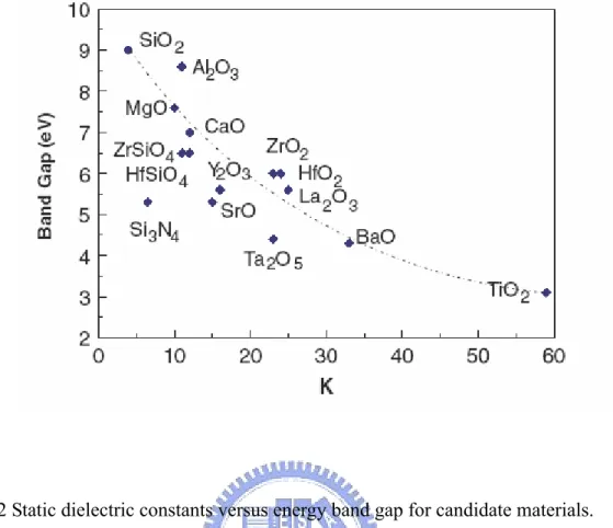
(15) 3. Low conduction for low leakage and low power consumption. For metal oxides (MOx), it is well known that bandgap is inversely related to κ value (the aluminum oxide as an exception). Low leakage current implies large band-offset for electrons and holes. 4. High carrier mobility at the dielectric/Si interface. Therefore, the low Dit and low bulk charges (low effective fixed charges) are requirements. 5. High breakdown strength and acceptable reliability. The breakdown strength is inversely related to κ value for metal oxides. 1.1.3 K Values and Thermal Stability The oxide’s K value should be over 12, preferably 25–30. There is a trade off with the band offset condition, which requires a reasonably large band gap to reduce gate leakage currents. Table 1-1 and figure 1-2 show that the K of candidate oxides varies inversely with the band gap. In fact, a very large K is undesirable in CMOS design because of large fringing fields at the source and drain electrodes [1-5]. The oxide must not react with Si to form either SiO2 or a silicide according to the unbalanced reactions. MO2 + Si → M + SiO2. (1). MO2 + 2Si → MSi + SiO2. (2). This is because the resulting SiO2 layer would increase the EOT and negate the effect of using the new oxide. In addition, any silicide formed by (2) is metallic and would short out. 3.
(16) the field effect. An interfacial layer of SiO2 often exists between the Si channel and the high. κ oxide layer [1-5~1-8]. There are advantages and drawbacks to this interfacial layer, as long as its presence and thickness can be controlled. The overall EOT of a layer 1 of SiO2 and a layer 2 of high κ oxide is given by the series capacitance formula (3), which becomes formula (4).. 1/C=1/C1+1/C2. (3). EOT=tSiO2+EOThiκ. (4). 1.1.4 Crystalline or amorphous oxides Unlike silicon oxide which is amorphous up to 1100℃ because of its low coordination covalent bonds, High-κ transition metal oxides are generally poor glass former. This is because the metal oxide bonding is normally a high coordination ionic bond with the d-state electrons and the oxide films crystallize easily at low temperatures. For both HfO2 and ZrO2, crystallization temperature was expected to be above 900℃. However, the real crystallization temperature is much lower of expected values. This difference may contribute to impurities or some sort of nucleation centers. Thus following post-deposition thermal treatment (PDA) will result in a certain degree of local crystallization. Nevertheless, structural defects in as-deposited. amorphous. films. can. be. removed. through. thermal. annealing. in. oxygen-containing ambient. Large amount of shallow oxide traps at the grain boundaries of the crystalline phase will be introduced at the same time. As a result, crystallization will give rise to a large leakage current because of large amount grain boundary traps [1-8]. 4.
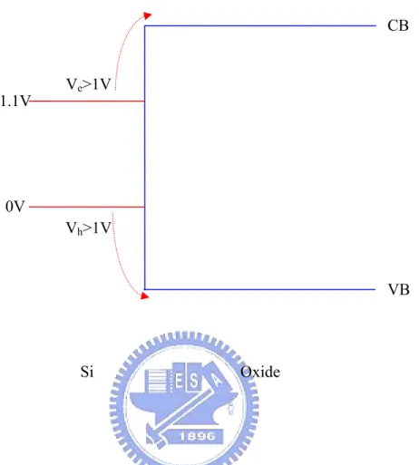
(17) 1.1.5 Band offset In order to decrease the leakage current, this requires that the potential barrier at each band must be over 1 eV in order to inhibit conduction by the Schottky emission of electrons or holes into the oxide bands, as shown schematically in figure 1-3. However, the reported high-κ materials usually have large leakage current. The large leakage current can be partially attributed to the small conduction band offset energy with respect to the silicon. The small conduction band offset does not only result in large gate direct-tunneling or Fowler–Norheim (FN) current but also give rise to large hot-carrier emission into the gate insulator. This limits the choice of oxide to those with band gaps over 5 eV. Only few materials like Al2O3, ZrO2, HfO2, Y2O3, and La2O3 and various lanthanides and their silicates and aluminates satisfy these requirements. These oxides also have excellent thermal stability. This is because a high heat of formation correlates with a wide band gap in ionic compounds [1-8].. 5.
(18) 1.2 Motivation to Study Metal Gate 1.2.1 Introduction Considerable challenges are encountered when bulk CMOS devices are scaled into the sub-100 nm regime for higher integrated circuit (IC) density and performance. The problems of polysilicon (poly-Si) gate depletion, high gate resistance, high gate tunneling leakage current, and boron penetration into the channel region become more severe as the channel length and gate-oxide thickness are aggressively reduced. In present CMOS, the gate electrodes are not real metals but polycrystalline Si doped highly n-type or p-type, respectively, for NMOS and PMOS. Their workfunctions are 4.05 eV and 5.15 eV, respectively, just as those required. The gate metals to be used must be ‘band edge metals’, with workfunctions equal to the band edge energies of Si, 4.05 and 5.15 eV [1-17]. 1.2.2 The Choice of Metal Gates As the device continuously scaling down, we encountered a lot of difficulties. Such gate electrodes have problems of: (1) Boron penetration into channels through thin gate dielectric. (2) High gate resistance. (3) Polysilicon gate depletion. (4) High gate tunneling leakage current. The possible solution is to use the proper metal gate with proper work function. The. 6.
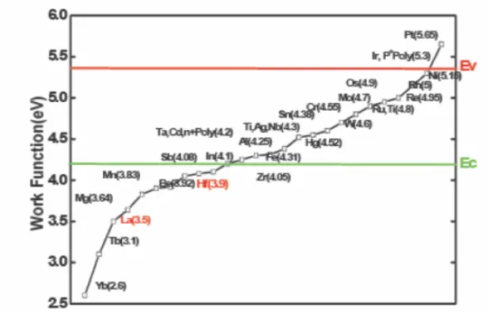
(19) parasitic series capacitance due to a depletion in poly crystalline-silicon gates poly gates reduce the gate capacitance and drive current. The metal gate electrode will make poly-depletion free due to the poly depletion will reduce the capacitance and contribute a degradation to EOT in inversion state. The work functions (Φm) of metal play an important role for metal-gate/high- κ MOSFET and are shown in Fig. 1-4. Metal gates with workfunctions near the conduction and valence band edges of Si are used in N- and P-MOSFETs respectively. To achieve the desired dual-metal gate workfunctions on high-κ gate dielectrics, candidate metals need to have vacuum workfunctions smaller (larger) than 4.05eV (5.17 eV) for the NMOS (PMOS). For the PMOS gate, inert metals must be used and this makes gate etching particularly challenging. Reactive metals have to be used as the NMOS gate, and this might introduce extrinsic interface states due to defects arising from an interfacial reaction [1-6]. There are more metal candidates for NMOSFET (Ti, Al, and Ta) than for PMOSFET. Among the possible candidates for PMOSFET, Pt and Ir are very difficult to etch using plasma processes. On the other hand, thermal stability of the effective metal electrode and metal diffusion are also important considerations. Recently, lots of metal or metal-nitride materials have been widely researched and successfully intergraded in advanced CMOSFET’s, such as TiN, TaN, Pt, Mo and Ir . Tantalum (Ta) has a work-function close to n+ poly-Si. Tantalum nitride (TaN) is quite stable (to maintain thermal stability up to a 1000℃ RTA) because the activation. 7.
(20) energy of metal and nitrogen is relatively low. Tantalum is bonded tightly within nitride and no obvious diffuse was observed in fabricated devices. However, TaN gate on high-κ HfO2 shows a significant shift of flat band voltage (VFB) toward the mid-gap of Si due to the interface reaction between the TaN and HfO2 at the high temperature. This is called the “Fermi-level pinning effect.” Therefore, the Fermi-level pinning effect needs to be avoided by selecting suitable metal gate and high-κ materials for advanced MOSFETs [1-7]-[1-9].. 8.
(21) 1.3 The Study of Fermi Level Pinning 1.3.1 Introduction In order to decrease the threshold voltage with the device scaling down, we have to choose metals with proper workfunctions carefully. The identification of metal-gate materials is very difficult because metal-gate workfunctions are observed to vary with different gate dielectrics and the process parameter. These intrinsic states are predominantly donor-like close to Ev, and mostly acceptor-like near Ec as shown in Fig. 1-5. Charge transfer generally occurs across the interface due to the presence of intrinsic interface states. Charging of these interface states creates a dipole that tends to drive the band lineup toward a position that would give zero dipole charge. Figure 1-5 illustrates the case where the metal Fermi level ΦF,m is above the charge neutrality level in the dielectric ECNL,d , creating a dipole that is charged negatively on the dielectric side. This interface dipole drives the band alignment so that EF,m goes toward ECNL,d and the effective metal work function, Φm,eff therefore differs from the vacuum metal work function Φm,vac. This work function change is proportional to the difference between ECNL,d and EF,m, or, equivalently, the difference between Φm,vac and ΦCNL,d [= (EVac-ECNL,d)/q ]. For some gate materials, there are no defects in the interface, and the workfunctions are determined by intrinsic states. According to reported paper, the workfunctions with Fermi-Level pinning effect are affected by annealing temperature. The Fermi level pinning effect is more obvious at higher temperature. The workfunctions would converge at higher. 9.
(22) temperature [1-8]-[1-10]. 1.3.2 The Effective Workfunctions We will discuss about the problems of the workfunctions shifts in the chapter. The workfunctions in vacuum are used as references. In the Schottky limit and without fixed charges, the flat band voltage of a MOS capacitor is given by equation (5). Inverting this equation, an effective workfunction of the gate metal ( Φ m, eff ) can be derived from the measured flat band voltage of the CV plot of the MOS capacitor, by referencing to the by referencing to the workfunction Φ s of the Si substrate, 4.05V or 5.15V for a n-type or p-type Si, respectively. We defined a pinning factor as the change of flat band voltage divided by the change in the metal’s vacuum workfunction as equation (7). Linearizing this model leads to another definition of effective workfunction, Φ m, eff , as shown in equation (8). In equation (8), Φ m, vac is the vacuum or true workfunction of metals and Φ CNL , d is the CNL energy of the oxide, measured from the vacuum level.. VFB = Φm − Φs. (5). Φm , eff = VFB + Φs. (6). S=dΦFB/dΦm. (7). Φm , eff = ΦCNL , d + S (Φm , vac − ΦCNL , d ). (8). S is a slope parameter that accounts for dielectric screening and depends on the electronic component of the dielectric constant ε∞ .The factor decreases as the dielectric permittivity becomes larger. The slope parameter S obeys an empirical relationship given by 10.
(23) equation (9). Materials with a smaller S tend to have obvious Fermi-Level pinning and the effective workfunction would approach Φ CNL , d , and the maximum value for S is unity, which indicates that no pinning of the metal Fermi level occurs [1-8]-[1-10]. S=. 1 1 + 0.1(ε∞ − 1) 2. (9). 11.
(24) 1.4 Fully-Silicided Gates High-performance CMOS technology generally requires two different workfunctions for n-MOS and p-MOS devices. This condition results in complex gate stacks and complex process. Only one kind of gate dielectrics deposited is basically required. One of the approaches uses a single metal layer, which sets workfunction for one type of transistor and an alloy of the same metal formed from an additional layer for the other transistor. An excellent technique, compatible with very large scale integrated VLSI CMOS technology of forming tunable metal gates by full silicidation FUSI of doped polysilicon gates, was recently demonstrated. The ability to form a pileup of dopant at the silicide/dielectric interface and thus to modulate the gate electrode workfunction appears to be strongly related to the silicidation conditions [1-11]. It is widely reported that the silicidation temperature and the ratio of Si and Ni thickness, affect the phase of the FUSI gate. Formation of dopant pileup in front of advancing silicide and ultimately at the silicide/gate dielectric interface is depend on what the diffuse species are. Virtually immobile dopant atoms in silicon at silicidation temperatures pile-up at the silicide front when silicon is the moving specie. Ni-rich silicides such as Ni2Si form by Ni atoms moving into Si, thus there is no dopant pileup. The pileup formed during NiSi formation implies that Si is moving specie during process. This phenomena is counter to Ni reacted with undoped Si. We would suggest that the presence of immobile dopant may be the key point of the FUSI gates. Several groups have been recently. 12.
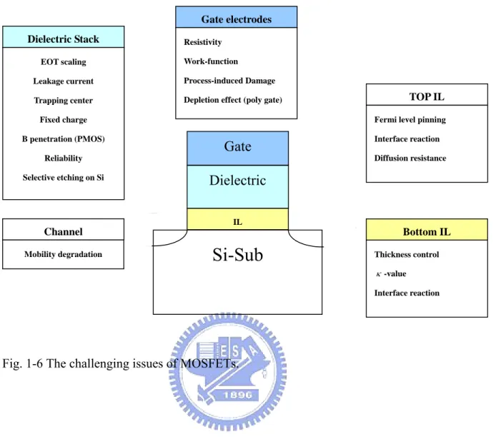
(25) studied FUSI gates on high-k dielectrics. Metal gates are proved to decrease severe Fermi level pinning observed on polysilicon/Hf-based dielectric stacks, believed to have been caused by Si-Hf interaction. No pinning was also reported for NiSi-HfAlNO system and for NiSi on HfO2. However, some studies show that FUSI NiSi does exhibit the pinning. It has been reported for NiSi gates on Hf silicate, NiSi and PtSi on HfOxN, and for NiSi on HfSiON. So we have to improve the stack formation process, and particularly the type and quality of interface between metal and dielectric to have better performance [1-11]-[1-15]. In Fig. 1-6, we summarize all the challenges of MOSFETs mentioned in Chapter 1.. 13.
(26) Materials. SiO2. Si3N4. Al2O3. HfSiO4. ZrO2. HfO2. La2O3. κ. 3.9. 7. 9. 11. 25. 25. 30. Table.1-1 Static dielectric constant (K) of various materials.. 14.
(27) Fig. 1-1 The ITRS Roadmap for semiconductor 2007.. 15.
(28) Fig. 1-2 Static dielectric constants versus energy band gap for candidate materials.. 16.
(29) CB. 1.1V. Ve>1V. 0V Vh>1V. VB. Si. Oxide. Fig. 1-3 Schematic of band offsets determining carrier injection in oxide band states.. 17.
(30) Fig. 1-4 The values of work function for different metal materials.. 18.
(31) Fig.1-5 Energy band diagram (left) and charging character of interface states (right) for the metal-dielectric interface.. 19.
(32) Gate electrodes Dielectric Stack EOT scaling. Resistivity Work-function. Leakage current. Process-induced Damage. Trapping center. Depletion effect (poly gate). Fermi level pinning. Fixed charge B penetration (PMOS). Gate. Interface reaction Diffusion resistance. Reliability Selective etching on Si. TOP IL. Dielectric IL. Channel Mobility degradation. Bottom IL. Si-Sub. Thickness control. κ -value Interface reaction. Fig. 1-6 The challenging issues of MOSFETs.. 20.
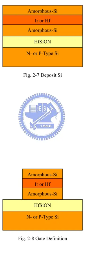
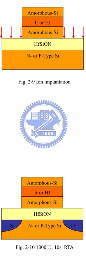
(33) Chapter 2 The Experimental Procedure 2.1 The Fabrication Step The gate-first IrxSi/HfSiON p-MOSFETs and HfxSi/HfSiON n-MOSFETS were fabricated on 12-in N-type Si wafers with resistivity of 1–10 Ω・ cm. After RCA cleaning, 4-nm HfSiO dielectric (Hf / (Hf + Si) =50%) was deposited by atomic-layer deposition (ALD). HfSiON gate dielectric was formed by applying NH3 plasma surface nitridation on HfSiO. For p-MOSFETs, 5–30-nm amorphous Si and 20–30-nm Ir were deposited by physical vapor deposition (PVD) [2-1]. For Ir/Si/HfSiON capacitors, a 1000℃ RTA was applied for 10 s to form IrxSi gates. For MOSFETs, additional 400-nm Si was deposited on top of Ir/Si to avoid ion implantation penetrating through the thin Ir/Si. After gate definition, Boron was implanted at 25-KeV energy and 5 × 1015 cm−2 dose, and activated at 1000℃ RTA for10 s. Meanwhile, IrxSi was also formed during RTA, where the x = 3 was determined by X-ray diffraction measurements. For n-MOSFETS, amorphous Si with various thickness of 50 to 5 nm was deposited on HfSiON as a silicide layer and metal barrier for subsequently deposited 20-nm-thick Hf by physical vapor deposition (PVD) [2-3]. The MOS capacitor was formed by patterning and RTA at 1000℃ for 10 s. Then, additional 150-nm-thick amorphous Si was deposited on Hf/Si/HfSiON to prevent ion implantation penetration, where the n+ source–drain regions are 21.
(34) formed by using a phosphorus ion implantation at 35 KeV. Then, the 1000 ◦C RTA was applied to activate the implanted dopant and the n-MOSFET was fabricated by this self-aligned gate first process. At such high 1000℃ RTA temperature, the fast silicidation reaching to the Si/HfSiON interface may also reduce the reaction of thin amorphous Si (5 nm) with high- κ dielectric to cause Fermi-level pinning.. 22.
(35) 2.2 The Measurement of MOSFET We used ion-mass spectroscopy (SIMS) to measure the Ir distribution profile. The fabricated p-MOSFETs and n-MOSFETs were further characterized by capacitance–voltage (C–V) and current–voltage (I–V) measurements. The capacitance–voltage (C–V) and current–voltage (I–V) measurements are measured by HP 4156C semiconductor parameter analyzer and HP 4284A precision LCR meter. In order to compare, Al, Ir-gated, and Hf-gated MOS capacitors on HfSiON were also fabricated. To prevent the different oxide charge from causing error in Φ m, eff extraction, HfSiON was subjected to the same thermal cycle (1000. ℃ RTA for 10 s) before Al gate deposition.. 23.
(36) 2.3 Process Flow. N- or P-Type Si. Fig. 2-1 N- or P-Type Si Substrate. N- or P-Type Si. Fig. 2-2 RCA clean. 24.
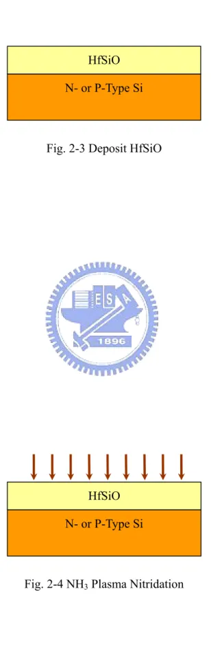
(37) HfSiO N- or P-Type Si. Fig. 2-3 Deposit HfSiO. HfSiO N- or P-Type Si. Fig. 2-4 NH3 Plasma Nitridation. 25.
(38) Amorphous-Si HfSiON N- or P-Type Si. Fig. 2-5 Deposit Amorphous-Si. Ir or Hf Amorphous-Si HfSiON N- or P-Type Si. Fig. 2-6 Deposit Ir or Hf. 26.
(39) Amorphous-Si Ir or Hf Amorphous-Si HfSiON N- or P-Type Si. Fig. 2-7 Deposit Si. Amorphous-Si Ir or Hf Amorphous-Si HfSiON N- or P-Type Si. Fig. 2-8 Gate Definition. 27.
(40) Amorphous-Si Ir or Hf Amorphous-Si HfSiON N- or P-Type Si. Fig. 2-9 Ion implantation. Amorphous-Si Ir or Hf Amorphous-Si HfSiON S. N- or P-Type Si. D. Fig. 2-10 1000℃, 10s, RTA. 28.
(41) Amorphous-Si Ir3Si or HfSix HfSiON S. N- or P-Type Si. D. Fig. 2-11 Fabricated MOSEFET. 29.
(42) Chapter 3 The Characteristics and Analysis of P-MOSFET 3.1 Introduction We have measured the J-V characteristics of the MOSFETs, and then want to find out their threshold voltages by using equation (10). W. ID =. COX µ eff (VG − VTH −. L. ∂ID ∂VD. gD =. VD. (10). )VD. 2. |. VG. (11). = CONSTANT. Measure IDS versus VGS curve with VS=0V, VB=0V, and VD<<VG-VTH. Make the IDS versus. VGS plot. There is a linear region at the neighboring of VGS at which gm, lin is maximum. The X-axis intersection is VGS =VTH +. VD , and we could find out the VTH. Then we want to find out 2. the mobility. Using equation (11) finds out the gd in linear region, and equation (12) gives the effective mobility.. µ eff =. gdL WQn. (12). VG. Qn =. ∫C. GC. dVG. (13). −∞. 3.2 The Effective Metal Workfunctions. We have fabricated three different kinds of gate electrodes. The three materials are IrxSi, Ir, and Al. Fig 3.1 and Fig. 3.2 shows the measured C–V characteristics of IrxSi, Ir, and Al gates on HfSiON MOS devices. We use low-temperature Al-gated HfSiON capacitors as a. 30.
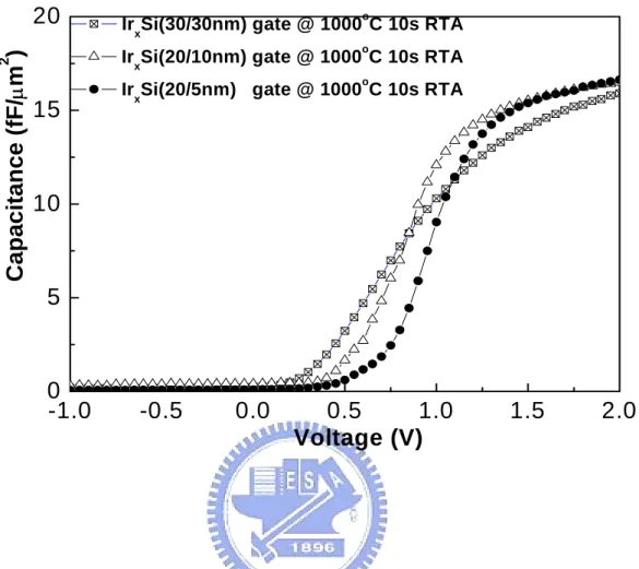
(43) reference because pure metal deposited at low temperature has less interface reaction with high-κ dielectrics than high-temperature process. The Al-gated HfSiON capacitors have fewer extrinsic states, and thus the Fermi-level pinning effect is not obvious in the structure [3-4].. Vfb = Φms − Qf / Cox = (Φm − Φs ) − (Qf / ε 0κ ox )tox. = (Φm − Φs ) − (Qf / ε 0κ sio 2) EOT. (14). The flat band voltage (Vfb) is expressed as equation (14), where Φm and Φs are the work functions for metal gates and Si, respectively. Qf , Cox, tox, and equivalent-oxide thickness (EOT) are the oxide charge, capacitance, physical thickness, and EOT for high-κ dielectrics. Since the three kinds of MOS devices have the same thermal cycle (1000 ◦C RTA for 10 s) before gates formation, we could assume that the fixed charge (Qf) amount should be the same. In Fig 3-2, the various flat band voltages (Vfb) may be due to the different metal work functions. Therefore, the principal effect of Vfb shift might be due to the difference of effective workfunction (Φm,eff ). The processes before gate definition are the same, and the MOS capacitors all have EOT values of 1.6nm. The shifts of C–V curves with different gate electrodes are attributed to the different work functions (Φm,eff ). Ir/HfSiON after 900 ◦C RTA has a large Vfb shift of 1.15 V to Al gates (Φm,eff = 4.1eV). It results in the required high. Φm,eff of 5.25 eV. This work-function value is also close to 5.27 eV for Ir. The pure metal Ir gates showed no obvious pinning effect. This is due to weak bonding strengths of Ir–O or Ir–N that reduce the Fermi-level-pinning-related interface reaction. However, we observed. 31.
(44) that Ir/HfSiON capacitors failed after 1000℃ RTA. 3.3 Thermal Stability. In Fig 3-3, Ir/HfSiON is failed after 1000℃ RTA. In order to activate the impurities, the gates have 1000℃ RTA after S/D implantation. To improve thermal stability, additional amorphous Si of 5–30 nm was inserted between Ir and HfSiON and also serve as a metal diffusion blocking layer. After 1000℃ RTA, IrxSi gate is formed. Good C–V characteristics were measured for IrxSi/HfSiON devices after the required 1000℃ RTA, although thermal stability was traded off at the Fermi-level pinning. In Fig 3-1, we obtained a high Φm,eff of 4.95 eV for IrxSi/HfSiON devices with the inserted 5-nm amorphous Si. Slow depletion for IrxSi /HfSiON devices with 30-nm amorphous Si may be due to nonuniform silicidation as examined by TEM, where locally unreacted Si was found to cause voltage drop in gate electrodes. The formation of FUSI gates is evident from the same inversion and accumulation capacitances measured in MOSFETs. 3.4 The J-V Characteristics. After 1000 ◦C RTA, Ir/HfSiON devices had high leakage currents and failed thus as shown in Fig. 3.3. On the other hand, IrxSi gates on HfSiON successfully improved thermal stability to 1000 ℃ RTA with low leakage current comparable with p+ poly-Si gates. 1000 ◦C RTA is required for dopant activation after ion implantation of source and drain. The measured large Vfb shift of IrxSi is supported by SIMS profile, as shown in Fig. 3-5. Here, Ir. 32.
(45) segregation toward amorphous Si formed IrxSi on HfSiON surface. Therefore, good thermal stability of 1000 ◦C RTA, a reasonable high Φm,eff of 4.95 eV, and a low gate dielectric leakage current can be achieved in IrxSi /HfSiON MOS capacitors at the same time. These are the few methods to achieve a high Φm,eff in Hf-based oxide p-MOS devices. There is a widely studied tuning method by impurity segregation in FUSI/SiON. However this method can not be applied to high-κ metal oxide due to the stronger interface reaction. In the following, we will study IrxSi /HfSiON devices with the thinnest 5-nm amorphous Si which has the best performance in the experiments. Compared with p-MOSFET, the Vfb of thicker Si layer is too low. Fig. 3-6 shows the transistor Id – Vd characteristics as a function of Vg - Vt for 1000 ◦C RTA IrxSi/HfSiON p-MOSFETs. The splendid results of Id – Vd curves of IrxSi/HfSiON transistors in Fig. 3-4 show little device performance degradation. Fig. 3-7 shows the Id – Vg characteristics of IrxSi-gated p-MOSFETs with HfSiON as the gate dielectric. In this work, we obtained the low Vt of −0.15 V from the linear Id – Vg plot, which is consistent with the large Φm,eff of 4.95 eV from C–V curves and the Ir accumulation on HfSiON from SIMS. Fig. 3-8 shows the extracted hole mobilities versus gate electric fields from the measured Id – Vg data of IrxSi/HfSiON p-MOSFETs. High hole mobilities of 84 and 53 cm2/V • s are obtained at peak value and 1 MV/cm effective field for. IrxSi/HfSiON p-MOSFETs, respectively, which is compatible with the published data in the literature [3-4]. Good hole mobility also indicates low Ir diffusion through HfSiON to. 33.
(46) inversion channel, even though excess Ir is necessary to prevent unreacted amorphous Si from causing gate depletion or increased Fermi-level pinning. Therefore, a highΦm,eff , a small Vt , and good hole mobility are achieved in IrxSi/HfSiON p-MOSFETs.. 34.
(47) o. IrxSi(30/30nm) gate @ 1000 C 10s RTA o. IrxSi(20/10nm) gate @ 1000 C 10s RTA. 2. Capacitance (fF/µm ). 20. o. 15. IrxSi(20/5nm) gate @ 1000 C 10s RTA. 10. 5. 0 -1.0. -0.5. 0.0. 0.5 1.0 Voltage (V). 1.5. 2.0. Fig. 3-1 C–V curves of HfSiON/n-Si with various Si thickness. The device areas are 100 × 100 µm.. 35.
(48) 20. o. IrxSi(20/5nm) gate @ 1000 C 10s RTA. 2. Capacitance (fF/µm ). o. Ir gate @ 900 C 10s RTA low temperture Al gate reference. 15. 10. 5. 0 -1.0. -0.5. 0.0. 0.5 1.0 Voltage (V). 1.5. Fig. 3-2 C–V curves of Ir/HfSiON, IrxSi/HfSiON (20/5nm), and Al/HfSiON.. 36. 2.0.
(49) 2. 10. 0. 2. Gate Current ( A/cm ). 10. 10. -2. 10. -4. 10. -6 o. 10. Ir gate @ 900 C 10s RTA o Ir gate @ 1000 C 5s RTA (failed). -8. 0.0. 0.5. 1.0 Voltage (V). 1.5. 2.0. Fig. 3-3 Ig-Vg curves of Ir/HfSiON/n-Si with RTA temperatures of 1000℃ and 900℃.. 37.
(50) 2. Gate Current ( A/cm ). 10. 2. 10. 0. 10. -2. 10. -4. 10. -6. low temperature Al gate reference o Ir xSi(30/30nm) gate @ 1000 C 10s RTA o. Ir xSi(20/10nm) gate @ 1000 C 10s RTA o. 10. Ir xSi(20/5nm) gate @ 1000 C 10s RTA. -8. 0.0. 0.5. 1.0 Voltage (V). Fig. 3.4 Ig-Vg curves of IrxSi/HfSiON and Al/HfSiON.. 38. 1.5. 2.0.
(51) Intensity (counts). 10. 10. 6. o. Si (RTA1000 C) o Si (RTA950 C) o Si (RTA900 C) o Ir (RTA1000 C) o Ir (RTA950 C) o Ir (RTA900 C). 5. Ir 3Si HfSiON Ir accum ulation. 10. 4. 10. 3. Ir. 0. 50. accumulation toward HfSiON. 100 150 Sputter Time (sec). 200. Fig. 3-5 SIMS profile of Ir3Si gates on HfSiON at different RTA temperatures. The Ir3Si that accumulated toward HfSiON interface is found to unpin the Fermi level.. 39.
(52) 4.0. |V g-V T |=0 V. Ir3 Si/HfSiON p-MOSFET 3.5. |V g-V T |=0.5 V. Gate length = 10 µ m. |V g-V T |=1 V. Id (mA). 3.0. |V g-V T |=1.5 V. 2.5 2.0 1.5 1.0 0.5 0.0 -2.5. -2.0. -1.5. -1.0. V d (V). Fig. 3-6 Id–Vd curves of Ir3Si/HfSiON p-MOSFETs.. 40. -0.5. 0.0.
(53) Id (A). 10. -3. 10. -4. 10. -5. 10. -6. 10. -7. 10. -8. 10. -9. 10. Ir3Si/HfSiON p-MOSFET. V ds = -0.1 V Gate length = 10 µ m. -10. -3.0. -2.5. -2.0. -1.5. -1.0. V g (V). Fig. 3-7 Id–Vg curves of Ir3Si/HfSiON p-MOSFETs.. 41. -0.5. 0.0. 0.5. 1.0.
(54) 200 Universal Ir3Si/HfSiON p-MOSFET. 2. µeff (cm /V-sec). 160. 120. 80. 40 -1.0. -0.8. -0.6. -0.4. -0.2. 0.0. Effective field (MV/cm). Fig. 3-8 Extracted hole mobilities from Id–Vg characteristics of Ir3Si/HfSiON p-MOSFETs.. 42.
(55) Chapter4 The Characteristics and Analysis of N-MOSFET 4.1 The Effective Metal Workfunctions and Thermal Stability. Fig. 4-1, Fig. 4-2, and Fig. 4-3 shows the C–V and J–V characteristics for HfSix/HfSiON and Al/HfSiON capacitors, where the HfSix gate was formed at 1000℃ RTA. The Al-gated capacitor has work-function of 4.1 eV. For various amorphous Si of 50 and 10 nm on HfSiON, the capacitance density decreases as the thickness of amorphous Si increases. This implies that not all amorphous silicon is silicided in HfSix gate on HfSiON. Thus a higher flat-band voltage (VFB ) due to the Fermi-level pinning on high-κ dielectric occurs. In contrast, the HfSix with thin 5-nm amorphous Si has the same capacitance density with Al gate. It is indicated that all amorphous Si is silicided. From the C–V shift referenced to the control Al gate, an extracted Φm,eff of 4.27 eV is obtained for HfSix/HfSiON. This result approaches the desired workfunction (Φm ) of NMOSFET. The low VFB and Φm,eff for HfSix gate capacitors with 5-nm amorphous Si may be due to the Hf diffusion toward the HfSiON surface through thin amorphous Si that decreases the work function. In addition, low leakage current of 1.9 × 10⁻⁵A/cm at −1 V is measured at an equivalent oxide thickness (EOT) of 1.6 nm. This result shows the good thermal stability of HfSix gate on HfSiON dielectric after 1000℃ RTA. Therefore, the experiment obtained reasonable low Φm,eff of 4.27 eV and a low gate leakage. 43.
(56) current in HfSix/HfSiON MOS capacitors at the same time [4-5]. 4.2 J-V Characteristics. Fig. 4-4 shows the transistor ID –VD characteristics as a function of Vg –Vt for the 1000 ℃ RTA-annealed HfSix/HfSiON n-MOSFETs. Fig. 4-5 displays ID –Vg characteristics of the. HfSix/HfSiON n-MOSFETs. A low Vt of only 0.14 V was measured from the linear ID –Vg plot, which agrees with the low Φm,eff of 4.27 eV from the C–V measurements. Fig. 4-6 shows the electron mobility extracted from the measured ID –Vg curves of the n-MOSFETs. A peak electron mobility of 216cm2/V·s was obtained for the HfSix/HfSiON n-MOSFETs.. 44.
(57) 25. o. HfSiX(20/50nm)@1000 CRTA o. 2. Capacitance (fF/µm ). HfSiX (20/10nm)@1000 CRTA. 20. o. HfSiX(20/5nm)@1000 CRTA. 15 10 5 0 -2.0. -1.5. -1.0 -0.5 Voltage (V). 0.0. 0.5. 1.0. Fig. 4-1 C–V characteristics for high-temperature RTA formed HfSix/HfSiON with various amorphous Si.. 45.
(58) 2. Capacitance (fF/µm ). 25. Al gate o HfSiX(20/5nm)@1000 CRTA. 20 15 10 5 0 -2.0. -1.5. -1.0 -0.5 Voltage (V). 0.0. 0.5. 1.0. Fig. 4-2 C–V characteristics for high-temperature RTA formed HfSix (20/5nm) HfSiON and low-temperature Al/HfSiON capacitors.. 46.
(59) 2. Gate Current Density (A/cm ). 10. -2. 10. -4. 10. -6. 10. -8. Al gate @low Temperature o HfSiX(20/50nm)@1000 CRTA o. HfSiX (20/10nm)@1000 CRTA o. 10. -10. -2.0. HfSiX(20/5nm)@1000 CRTA. -1.5. -1.0 Voltage (V). -0.5. Fig. 4-3 Jg - Vg characteristics for high-temperature RTA formed HfSix/HfSiON and low-temperature Al/HfSiON capacitors.. 47. 0.0.
(60) 5.5 5.0. Id ( mA ). 4.5. Vg - VT = 0 V Vg - VT = 0.5 V. o. HfSiX(20/5nm)@1000 CRTA HfSix/HfSiON n-MOSFET. Vg - VT = 1 V. 4.0. Vg - VT = 1.5 V. 3.5. Vg - VT = 2 V. 3.0 2.5 2.0 1.5 1.0 0.5 0.0 0.0. 0.5. 1.0. 1.5 Vd (V). 2.0. 2.5. Fig. 4-4 ID –VD characteristics of HfSix/HfSiON n-MOSFET. The amorphous Si on HfSiON was 5 nm and gate length was 10 µm.. 48.
(61) Id (A). 10. -2. 10. -4. 10. -6. o. 10. HfSiX(20/5nm)@1000 CRTA. -8. HfSiX/HfSiON n-MOSFET V ds= 0.1 V. 10. -10. -1.0. -0.5. 0.0. 0.5 V g (V). Fig. 4-5 Id–Vg characteristics of HfSix/HfSiON n-MOSFET.. 49. 1.0. 1.5. 2.0.
(62) Universal HfSix/HfSiON n-MOSFET o HfSiX(20/5nm)@1000 CRTA. 600. 2. µeff (cm /V-sec). 800. 400. 200. 0 0.0. 0.2. 0.4 0.6 0.8 Effective field (MV/cm). Fig. 4-6 Electron mobility of HfSix/HfSiON n-MOSFETs.. 50. 1.0.
(63) Chapter5 Conclusion In the experiment, we have obtained good device performance of IrxSi/HfSiON p-MOSFETs with a high Φm,eff of 4.95 eV, a small Vt of −0.15 V, a peak hole mobility of 84 cm2/V・s, and 1000℃RTA thermal stability. For NMOSFET, a low Φm,eff of 4.27eV, threshold voltage of 0.14V, and a mobility of 216cm2/V·s are obtained. They are obviously that the processes can be integrated in current technology. On the other hand, we will study hard to decrease EOT by replacing the high- κ gate dielectrics in the future. The threshold voltages of devices are needed to decrease, and avoid the Fermi-Level pinning. However, the research of this work proved that this is an effective way to meet the ITRS roadmap after 2008.. 51.
(64) Reference Chap1:. [1-1] 廖金昌, “The Electrical Characteristics and Application in MOSFETs of High k Gate Dielectric Al2O3 Formed by Aluminum Oxidation”,交通大學,博士論文,九十四年二月。 [1-2] K. Mistry, C. Allen, C. Auth, B. Beattie, D. Bergstrom, M. Bost, M. Brazier, M. Buehler, A. Cappellani, R. Chau, C.-H. Choi, G. Ding, K. Fischer, T. Ghani, R. Grover, W. Han, D. Hanken, M. Hattendorf, J. He, J. Hicks , R. Huessner, D. Ingerly, P. Jain, R. James, L. Jong, S. Joshi, C. Kenyon, K. Kuhn, K. Lee, H. Liu, J. Maiz, B. McIntyre, P. Moon, J. Neirynck, S. Pae, C. Parker, D. Parsons, C. Prasad , L. Pipes, M. Prince, P. Ranade, T. Reynolds, J. Sandford, L. Shifren0, J. Sebastian, J. Seiple, D. Simon, S. Sivakumar, P. Smith, C. Thomas, T. Troeger, P. Vandervoorn, S. Williams, and K. Zawadzki, “A 45nm Logic Technology with High-k-Metal Gate Transistors, Strained Silicon, 9 Cu Interconnect Layers, 193nm Dry Patterning, and 100% Pb-free Packaging”, IEEE, pp.247-250, 2007. [1-3] A.L.P. Rotondaro, M.R. Visokay, J.J. Chambers, A. Shanware, R. Khamankar, H. Bu, R.T. Laaksonen, L.Tsung, M. Douglas, R. Kuan, M.J. Bevan, T. Grider, J. cPherson, L. Colombo, “Advanced CMOS Transistors with a Novel HfSiON Grate Dielectric”, Symposium On VLSI Technology Digest of Technical Papers, pp148-149, 2002. [1-4] D.A. Buchanan, E.P. Gusev, E. Cartier, H. Okorn-Schmidt, K. Rim, M.A. Gribelyuk, A. Mocuta, A. Ajmera, M. Copel, S. Guha, N. Bojarczuk, A. Callegari, C. D’Emic, P. Kozlowski, 52.
(65) K. Chan, R.J. Fleming, P.C. Jamison, J. Brown, R Arndt, IEDM Technical Digest (2000) 223. [1-5] E.P. Gusev, E. Cartier , D.A. Buchanan , M. Gribelyuk , M. Copel , H. Okorn-Schmidt , C. D’Emic, “Ultrathin high-K metal oxides on silicon: processing, characterization and integration issues” , Microelectronic Engineering 59, pp. 341–349, 2001. [1-6] Baohong Cheng, Min Cao, Ramgopal Rao, Anand Inani, Paul Vande Voorde, Wayne M. Greene, Johannes M. C. Stork, Zhiping Yu, Peter M. Zeitzoff, and Jason C. S. Woo, “The Impact of High- κ Gate Dielectrics and Metal Gate Electrodes on Sub-100 nm MOSFET’s”, IEEE TRANSACTIONS ON ELECTRON DEVICES, VOL. 46, NO. 7, pp.1537-1544, JULY 1999. [1-7] G. D. Wilk and R. M. Wallace, “Electrical properties of hafnium silicate gate dielectrics deposited directly on silicon”, APPLIED PHYSICS LETTERS VOLUME 74, NUMBER 19, pp.2854-2856. [1.8] John Robertson, “High dielectric constant gate oxides for metal oxide Si”, Rep. Prog. Phys. 69 (2006), pp. 327–396. [1-9] Yee-Chia, Yeo Tsu-Jae King, and Chenming Hu, “Metal-dielectric band alignment and its implications for metal gate complementary metal-oxide-semiconductor technology”, JOURNAL OF APPLIED PHYSICS VOLUME 92, NUMBER 12, pp.7276-7271. [1-10] H. Y. Yu, Chi Ren, Yee-Chia Yeo, J. F. Kang, X. P. Wang, H. H. H. Ma, Ming-Fu Li, D. S. H. Chan, and D.L. Kwong, “Fermi Pinning-Induced Thermal Instability of. 53.
(66) Metal-Gate Work Functions”, IEEE ELECTRON DEVICE LETTERS, VOL. 25, NO. 5, pp.337-339, MAY 2004. [1-11] M. Copel, R. P. Pezzi, and C. Cabral, Jr., “Interfacial segregation of dopants in fully silicided metal-oxide-semiconductor gates”, APPLIED PHYSICS LETTERS 86, 2005. [1-12] J. H. Sim, H. C. Wen, J. P. Lu, and D. L. Kwong, “Work Function Tuning of Fully Silicided NiSi Metal Gates Using a TiN Capping Layer”, IEEE ELECTRON DEVICE LETTERS, VOL. 25, NO. 9, SEPTEMBER 2004. [1-13] Kousuke SANO, Masaki HINO, Norihiro OOISHI and Kentaro SHIBAHARA, “Workfunction Tuning Using Various Impurities for Fully Silicided NiSi Gate”, Japanese Journal of Applied Physics Vol. 44, No. 6A, pp. 3774–3777, 2005. [1-14] T. Nabatame, M. Kadoshima, K. Iwamoto, N. Mise, S. Migita, M. Ohno, H. Ota, N. Yasuda', A. Ogawa, K. Tominaga, H. Satake and A. Toriumi, “Partial Silicides Technology for Tunable Work Function Electrodes on High-k Gate Dielectrics - Fermi Level Pinning Controlled PtSi, for HfO, (N) pMOSFET -”, in IEDM Tech. Dig., 2004, pp. 83-86. [1-15] Jakub Kedzierski, Diane Boyd, Paul Ronsheim, Sufi Zafar, J. Newbury, John Ott, Cyril Cabral Jr., M. Ieong, Wil6ied Haensch, “Threshold voltage control in NiSi-gated MOSFETs through silicidation induced impurity segregation (SIIS)”, in IEDM Tech. Dig., 2003, pp. 315-318. [1-16] M. R. Visokay, J. J. Chambers, A. L. P. Rotondaro, A. Shanware, and L. Colombo. 54.
(67) “Application of HfSiON as a gate dielectric material”, Appl. Phys. Lett., Vol. 80, No. 17, 29 April 2002. [1-17] Qiang Lu, Ronald Lin, Pushkar Ranade, Tsu-Jae Ring, Chenming Hu, “Metal Gate Work Function Adjustment for Future CMOS Technology”, Symp. on VLSI Tech., pp.45-46, 2001. [1-18] Qiang Lu, Yee Chia Yeo, Pushkar Ranade, Hideki Takeuchi, Tsu-Jae King, Chenming Hu, S. C. Song, H. F. Luan‘ and Dim-Lee Kwong, “Dual-Metal Gate Technology for Deep-Submicron CMOS Transistors”, Symp. on VLSI Tech., pp.72-73, 2000. [1-19] Chang Seo Park, Byung Jin Cho, and Dim-Lee Kwong, “Thermally Stable Fully Silicided Hf-Silicide Metal-Gate Electrode”, IEEE ELECTRON DEVICE LETTERS, VOL. 25, NO. 6, pp.372-374, JUNE 2004. [1-20] K. Ohmori , T. Chikyow, T. Hosoi, H. Watanabe, K. Nakajima, T. Adachi , A. Ishikawa, Y. Sugita, Y. Nara, Y. Ohji, K. Shiraishi, K. Yamabe, K. Yamada, “Wide Controllability of Flatband Voltage by Tuning Crystalline Microstructures in Metal Gate Electrodes”, IEEE, pp.345-348, 2007. [1-21] Wan Sik Hwang, Chen Shen, Xing Peng Wang, Daniel S. H. Chan, and Byung Jin Cho, “Wide Controllability of Flatband Voltage by Tuning Crystalline Microstructures in Metal Gate Electrodes”, in Symp. on VLSI Tech., pp.156-157, 2007. [1-22] J. Petry, R. Singanamalla, K. Xiong, C. Ravit, E. Simoen, R. O'Connor, A. Veloso, C.. 55.
(68) Adelmann , S. VanElshocht, V. Paraschiv, S. Brus, J. Van Berkum, S. Kubicek, K. De Meyer, S. Biesemans, J.C. Hooker, “Tuning PMOS Mo(O,N) metal gates to NMOS by addition of DyO capping layer”, IEEE, pp.329-332, 2007. [1-23] H. Shang, M. M. Frank, E. P. Gusev, J. O. Chu, S. W. Bedell, K. W. Guarini, M. Ieong “Germanium Channel MOSFETs: opportunities and challenges” IBM J. RES. & DEV. VOL. 50 NO. 4/5, pp.377-386, JULY/SEPTEMBER 2006 [1-24] E. P. Gusev, V. Narayanan, M. M. Frank, “Advanced high-κ dielectric stacks with polySi and metal gates: Recent progress and current challenges”, IBM J. RES. & DEV. VOL. 50 NO. 4/5, pp.387-410, JULY/SEPTEMBER 2006. [1-25] G. Ribes, J. Mitard, M. Denais, S. Bruyere, F. Monsieur, C. Parthasarathy, E. Vincent, and. G.. Ghibaudo,. “Review. on. High-k. Dielectrics. Reliability. Issues”,. IEEE. TRANSACTIONS ON DEVICE AND MATERIALS RELIABILITY, VOL. 5, NO. 1, pp.5-19, MARCH 2005. [1-26] Hei Wong, Hiroshi Iwai, “On the scaling issues and high-κ replacement of ultrathin gate dielectrics for nanoscale MOS transistors”, Microelectronic Engineering 83 1867–1904, 2006. Chap2:. [2-1] C. H. Wu, D. S. Yu, A. Chin, S. J. Wang, M.-F. Li, C. Zhu, B. F. Hung, and S. P. McAlister, “High work function IrxSi gates on HfAlON p-MOSFETs”, IEEE Electron Device. 56.
(69) Lett., vol. 27, no. 2, pp. 90–92, Feb. 2006.. [2-2] D. S. Yu, A. Chin, C. H. Wu, M.-F. Li, C. Zhu, S. J. Wang, W. J. Yoo, B. F. Hung, and S. P. McAlister, “Lanthanide and Ir-based dual metal gate/HfAlON CMOS with large work-function difference”, in IEDM Tech. Dig., pp. 649–652, 2005. [2-3] C. H. Wu, B. F. Hung, Albert Chin, S. J. Wang, F. Y. Yen, Y. T. Hou, Y. Jin, H. J. Tao, S. C. Chen, and M. S. Liang, “HfSiON n-MOSFETs Using Low-Work Function HfSix Gate”, IEEE ELECTRON DEVICE LETTERS, VOL. 27, NO. 9, pp.762-764, SEPTEMBER 2006. Chap3:. [3-1] C. H. Wu, D. S. Yu, A. Chin, S. J. Wang, M.-F. Li, C. Zhu, B. F. Hung, and S. P. McAlister, “High work function IrxSi gates on HfAlON p-MOSFETs”, IEEE Electron Device Lett., vol. 27, no. 2, pp. 90–92, Feb. 2006.. [3-2] T. Nabatame, M. Kadoshima, K. Iwamoto, N. Mise, S. Migita, M. Ohno, H. Ota, N. Yasuda, A. Ogawa, K. Tominaga, H. Satake, and A. Toriumi, “Partial silicides technology for tunable work function electrodes on high-κ gate dielectrics- Fermi-level pinning controlled PtSix for HfOx (N) pMOSFET”, in IEDM Tech. Dig., pp. 83–86, 2004. [3-3] K. Takahashi, K. Manabe, T. Ikarashi, N. Ikarashi, T. Hase, T. Yoshihara, H. Watanabe, T. Tatsumi, and Y. Mochizuki, “Dual workfunction Ni-silicide/HfSiON gate stacks by phase-controlled full-silicidation (PC-FUSI) technique for 45 nm-node LSTP and LOP devices”, IEDM Tech. Dig., pp. 91–94, 2004.. 57.
(70) [3-4] C. H. Wu, D. S. Yu, A. Chin, S. J. Wang, M.-F. Li, C. Zhu, B. F. Hung, and S. P. McAlister, “High work function IrxSi gates on HfAlON p-MOSFETs”, IEEE Electron Device Lett., vol. 27, no. 2, pp. 90–92, Feb. 2006.. [3-5] D. S. Yu, A. Chin, C. H. Wu, M.-F. Li, C. Zhu, S. J. Wang, W. J. Yoo, B. F. Hung, and S. P. McAlister, “Lanthanide and Ir-based dual metal gate/HfAlON CMOS with large work-function difference”, IEDM Tech. Dig., , pp. 649–652, 2005. [3-6] J. K. Schaeffer, C. Capasso, L. R. C. Fonseca, S. Samavedam, D. C. Gilmer, Y. Liang, S. Kalpat, B. Adetutu, H.-H. Tseng, Y. Shiho, A. Demkov, R. Hegde, W. J. Taylor, R. Gregory, J. Jiang, E. Luckowski, M. V. Raymond, K. Moore, D. Triyoso, D. Roan, B. E. White, Jr., and P. J. Tobin, “Challenges for the integration of metal gate electrodes”, in IEDM Tech. Dig., pp. 287–290, 2004. [3-7] B. Tavel, T. Skotnicki, G. Pares, N. Carrière, M. Rivoire, F. Leverd, C. Julien, J. Torres, and R. Pantel, “Totally silicided (CoSi2) polysilicon: A novel approach to very low-resistive gate (∼2Ω/_) without metal CMP nor etching”, IEDM Tech. Dig., pp. 815–828, 2001. [3-8] M. Koyama, Y. Kamimuta, T. Ino, A. Kaneko, S. Inumiya, K. Eguchi, M. Takayanagi, and A. Nishiyama, “Careful examination on the asymmetric Vfb shift problem for Poly-Si/HfSiON gate stack and its solution by the Hf concentration control in the dielectric near the Poly-Si interface with small EOT expense”, IEDM Tech. Dig., pp. 499–502, 2004. [3-9] H. B. Michaelson, “The work function of the elements and its periodicity”, J. Appl.. 58.
(71) Phys., vol. 48, no. 11, pp. 4729–4733, Nov. 1977.. [3-10] A. L. P. Rotondaro, M. R. Visokay, J. J. Chambers, A. Shanware, R. Khamankar, H. Bu, R. T. Laaksonen, L. Tsung, M. Douglas, R. Kuan, M. J. Bevan, T. Grider, J.Mcpherson, and L. Colombo, “Advanced CMOS transistors with a novel HfSiON gate dielectric”, VLSI Symp. Tech. Dig., pp. 148–149, 2002.. [3-11] W. P. Maszara, Z. Krivokapic, P. King, J. S. GooIlgweon, and M. R. Lin, “Transistors with dual work function metal gate by single full silicidation (FUSI) of polysilicon gates”, in IEDM Tech. Dig., pp. 367–370, 2002. Chap4:. [4-1] H.-H. Tseng, C. C. Capasso, J. K. Schaeffer, E. A. Hebert, P. J. Tobin, D. C. Gilmer, D. Triyoso, M. E. Ramón, S. Kalpat, E. Luckowski, W. J. Taylor, Y. Jeon, O. Adetutu, R. I. Hegde, R. Noble, M. Jahanbani, C. El Chemali, and B. E. White, “Improved short channel device characteristics with stress relieved pre-oxide (SRPO) and a novel tantalum carbon alloy metal stack,” IEDM Tech. Dig., pp. 821–824, 2004. [4-2] C. S. Park, B. J. Cho, L. J. Tang, and D. L. Kwong, “Substituted aluminum metal gate on high-κ dielectric for low work-function and Fermi-level pinning free,” in IEDM Tech. Dig., pp. 299–302, 2004. [4-3] D. S. Yu, K. C. Chiang, C. F. Cheng, A. Chin, C. Zhu, M. F. Li, and D. L. Kwong, “Fully silicided NiSi : Hf/LaAlO3/ Smart-Cut-Ge-On-Insulator n-MOSFETs with high. 59.
(72) electron mobility”, IEEE Electron Device Lett., vol. 25, no. 8, pp. 559–561, Aug. 2004. [4-4] C. Y. Lin, M. W. Ma, A. Chin, Y. C. Yeo, C. Zhu, M. F. Li, and D. L. Kwong, “Fully silicided NiSi gate on La2O3 MOSFETs”, IEEE Electron Device Lett., vol. 24, no. 5, pp. 348–350, May 2003. [4-5] A. Veloso, K. G. Anil, L. Witters, S. Brus, S. Kubicek, J.-F. de Marneffe, B. Sijmus, K. Devriendt, A. Lauwers, T. Kauerauf, M. Jurczak, and S. Biesemans, “Work function engineering by FUSI and its impact on the performance and reliability of oxynitride and Hf-silicate based MOSFETs”, in IEDM Tech. Dig., pp. 855–858, 2004. [4-6] S. J. Rhee, C. S. Kang, C. H. Choi, C. Y. Kang, S. Krishnan, M. Zhang, M. S. Akbar, and J. C. Lee, “Improved electrical and material characteristics of hafnium titanate multi-metal oxide n-MOSFETs with ultra-thin EOT (∼ 8 Å) gate dielectric application,” in IEDM Tech. Dig., pp. 837–840, 2004.. 60.
(73) Vita 姓名:黃俊哲 性別:男 出生年月日:民國 73 年 8 月 15 日 籍貫:台灣省台南縣 住址:台南縣佳里鎮安西里安西 56-32 號 學歷:國立清華大學工程與系統科學系 (民國 91 年 9 月~民國 95 年 6 月) 國立交通大學電子研究所固態電子組 (民國 95 年 9 月~民國 97 年 6 月). 論文題目: 金屬矽化物-高介電常數介電質-半導體場效應電晶體之電性研究. The Research of Electrical Characteristics of FUSI Gate-High- κ Dielectric-Semiconductor Field-Effect Transistor.. 61.
(74)
數據

+7

相關文件
導體 絕緣體 電解質 非電解質.
導體 絕緣體 電解質 非電解質.
細目之砂紙,將絕緣體 及內部半導電層鉛筆狀
• 接續之前的例子,若原為 0.288 pF 的液晶 電容 C LC ,再並聯一個亦為 0.288 pF 的電 容C st ,則電位保持的變化值為.
◦ 金屬介電層 (inter-metal dielectric, IMD) 是介於兩 個金屬層中間,就像兩個導電的金屬或是兩條鄰 近的金屬線之間的絕緣薄膜,並以階梯覆蓋 (step
10 Magnetism of Matter 磁 性 Electromagnetic Waves 電磁 波. How can a clay-walled kiln reveal
在室溫時,少部分共價鍵中的電子吸收了足 夠的熱能跳出他的鍵結位置,進入共價鍵間
雙極性接面電晶體(bipolar junction transistor, BJT) 場效電晶體(field effect transistor, FET).
