國
立
交
通
大
學
電子工程學系 電子研究所碩士班
碩
士
論
文
適用於高速時脈產生之低功率全數位式頻率合成器
A LOW POWER ADPLL-BASED FREQUENCY
SYNTHESIZER FOR HIGH SPEED CLOCK
GENERATION
研 究 生:楊宗熙
指導教授:黃 威 教授
適用於高速時脈產生之低功率全數位式頻率合成器
A LOW POWER ADPLL-BASED FREQUENCY
SYNTHESIZER FOR HIGH SPEED CLOCK
GENERATION
研 究 生:楊宗熙 Student:Zong-Xi Yang
指導教授:黃 威 教授 Advisor:Prof. Wei Hwang
國 立 交 通 大 學
電 子 工 程 學 系 電 子 研 究 所
碩 士 論 文
A Thesis
Submitted to Department of Electronics Engineering & Institute of Electronics College of Electrical Engineering and Computer Engineering
National Chiao Tung University in partial Fulfillment of the Requirements
for the Degree of Master
in
Electronics Engineering July 2006
Hsinchu, Taiwan, Republic of China
適用於高速時脈產生之低功率全數位式頻率合成器
學生:楊宗熙
指導教授:黃 威 教授
國立交通大學電子工程學系電子研究所
摘 要
本論文提出一個新的數位控制頻率振盪器及一個新的相位頻率偵測器之架 構以設計一個低功率的全數位式鎖相迴路。藉由使用一新型的數位控制延遲元 件,此顆數位控制頻率振盪器可具有其絕對單調的特性,且使的數位控制頻率振 盪器的設計更為容易。此外,我們也提出了一個新的相位頻率偵測器,它可以在 一個參考時脈週期內,完成頻率和相位的比較,並且能進一步調整振盪器的振盪 頻率。 此全數位式頻率合成器是以 TSMC 0.13um 技術來做設計。它的輸出頻率範 圍可從三百百萬赫茲到一千百萬赫茲,並且可以在十六個參考時脈週期內達到鎖 定(最差的情況下)。輸出時脈訊號的鋒對鋒抖動值亦可維持在 120ps 之內。在供 應電壓為 1.2 伏,操作頻率在 1 千百萬赫茲的情況下,此全數位式頻率合成器所 消耗的總功率為 3.1 毫瓦。此外,參考現有的高速時脈應用之規格,此頻率合成 器可作為高速數位訊號處理器的時脈產生器。A LOW POWER ADPLL-BASED FREQUENCY
SYNTHESIZER FOR HIGH SPEED CLOCK
GENERATION
Student :Zong-Xi Yang Advisor : Prof. Wei Hwang
Department of Electronics Engineering & Institute of Electronics
National Chiao-Tung University
ABSTRACT
This thesis proposes a new digital controlled oscillator (DCO) and a new phase frequency detector (PFD) architecture for the all digital phase-locked loop (ADPLL) with low power design. By using the new type digitally controlled delay element (DCDE), a digitally controlled oscillator (DCO) with characteristics of its monotonicity is presented, which makes the DCO design more straightforward. Besides, a new PFD architecture that can finish phase and frequency comparison and adjustment in one reference cycle is also presented.
The proposed ADPLL-based frequency synthesizer has been designed with TSMC 0.13um technology model. It can operate from 300 MHz to 1 GHz, and achieve frequency acquisition within sixteen reference clock cycles (worst case scenario). The peak-to-peak jitter of the output clock is less than 120 ps. Total power dissipation of the ADPLL-based frequency synthesizer is 3.1 mW at 1 GHz with a 1.2 V power supply. With the specification, it could be used for high speed clock
Acknowledgements
I am grateful to have many people assisting in supporting this thesis. This thesis would not be accomplished without them.
First of all, I would like to thank my advisor, Prof. Wei Hwang, who has provided me a good research environment and the complete support, which does help me be devoted to the study of this research topic independently. With his edification and judicious advices, I was inspirited in this knowledge field and also gained much significant experience.
Next, the fellows of my laboratory also help a lot on my thesis. They accompany me with delights and serious works, and it makes me own a colorful life in my years at NCTU.
Finally, I would also like to thank my family, for their concerns and understanding. With their encouragement and support, I could always stride forward without fear of disturbance in the rear. Thank you all.
Contents
Chapter 1 Introduction...1
1.1 Research Motivation ...1
1.2 Thesis Organization ...6
Chapter 2 An Overview of PLL ...8
2.1 The Operating Principle of PLL...9
2.2 Linear PLL ... 11
2.3 Digital PLL ...14
2.3.1 Phase Frequency Detector...15
2.3.2 Charge Pump/Loop Filter...18
2.3.3 Voltage Controlled Oscillator...20
2.3.4 Frequency Divider ...23
2.4 All Digital PLL ...25
2.5 An Example of The Conventional ADPLL Design...29
2.5.1 Architecture Overview ...29
2.5.2 Digitally Controlled Oscillator ...31
2.5.3 Frequency Acquisition ...34
2.5.4 Phase Acquisition...37
2.5.5 Phase and Frequency Maintenance ...39
Chapter 3 Digitally Controlled Oscillator...40
3.1 Basic Concepts of DCO ...40
3.2 Different Approaches for DCO design...41
3.3 Digitally Controlled Delay Element ...44
3.4 Digitally Controlled Oscillator Architecture...52
Chapter 4 A Low Power ADPLL Circuit Design ...56
4.1 Architecture of The ADPLL...56
4.2 Circuit Design of The ADPLL ...58
4.2.1 Phase/Frequency Detector ...58
4.2.2 Control Unit ...62
4.2.4 The Sub-Circuit Design ...65
Chapter 5 The Implementation of Frequency Synthesizer ....68
5.1 Frequency Synthesizer Architecture ...68
5.1.1 Integer-N Architecture ...69
5.2 Frequency Dividers ...73
5.2.1 Divide-by-Two Circuits ...74
5.2.2 Dual-Modulus Dividers ...75
5.3 The Proposed ADPLL-Based Frequency Synthesizer ...78
5.4 Layout Implementation and Simulation Result ...79
Chapter 6 Conclusion and Future Work ...94
6.1 Conclusion ...94
List of Figures
Fig.1-1 Frequency multiplication...2
Fig.1-2 Frequency synthesizer ...2
Fig.1-3 Skew between data and buffered clock ...3
Fig.1-4 Use of a PLL to eliminate skew ...4
Fig.1-5 (a) Retiming data with D flipflop driven by a low-noise clock ...5
(b) use of a phase-locked clock recovery circuit to generate the clock ...5
Fig.2-1 Block diagram of PLL...10
Fig.2-2 The transfer curve of VCO ...10
Fig.2-3 The transfer curve of PD ... 11
Fig.2-4 Linear PLL model ...12
Fig.2-5 Digital PLL Block ...15
Fig.2-6 Phase Frequency Detector Block ...16
Fig.2-7 (a) PFD response with input reference lagging feedback clock...16
(b) PFD response with freq. of input reference > that of feedback clock ...16
Fig.2-8 PFD state diagram ...17
Fig.2-9 Charge Pump and Loop Filter ...18
Fig.2-10 three kinds of passive Loop Filter ...19
Fig.2-11 The response of PFD and Charge Pump/Loop Filter ...19
Fig.2-12 LC-Tank Voltage-Controlled Oscillator ...22
Fig.2-13 five stage signal ended ring oscillator ...23
Fig.2-14 Divide-by-two using a TSPC register ...24
Fig.2-15 All Digital Phase-Locked Loop...26
Fig.2-16 The Conventional ADPLL Block Diagram ...30
Fig.2-17 (a) The Constituent DCO cell, (b) The Digitally Controlled Oscillator....33
Fig.2-18 The Frequency Comparator...36
Fig.2-19 Frequency Comparator Timing ...37
Fig.2-20 (a) Phase Acquisition Mux, (b) Phase Acquisition Resolved...38
Fig.3-1 DCO composed of a DAC and a VCO...41
Fig.3-2 DCO composed of a high frequency oscillator and a divider ...42
Fig.3-6 Basic structure of a delay element...46
Fig.3-7 Current-starved delay element ...47
Fig.3-8 Another delay element...48
Fig.3-11 The Modified DCDE ...53
Fig.3-12 DCO Frequency V.S. number of the input vector ...54
Fig.4-1 The ADPLL Block Diagram...57
Fig.4-2 The Modified Binary Search ...58
Fig.4-3 Phase/Frequency Detector...59
Fig.4-4 Timing diagram of the Phase/Frequency Detector ...60
(a) unlock state, (b) lock state (for example: divider ratio=2) ...60
Fig.4-5 DCO Enable Generator ...61
Fig.4-6 (a) Block diagram of the Control Unit ...63
(b) An example of the phase gain strategy...63
Fig.4-7 TSPC DFF ...66
Fig.4-8 1-bit FA (a) logic diagram, (b) transistor-level circuit ...67
Fig.4-9 11-bit modified ripple adder/subtractor...67
Fig.5-1 Pulse swallow frequency divider...69
Fig.5-2 (a) Simple fractional-N synthesizer, (b) use of divider in the loop ...72
Fig.5-3 Fractional-N synthesizer using a dual-modulus divider...72
Fig.5-4 Example of a fractional-N synthesizer ...73
Fig.5-5 Divide-by-two circuit ...74
Fig.5-6 Dynamic dividers using (a) inverters, (b) TSPC ...75
Fig.5-7 (a) Divide-by-3 circuit (b) Divide-by-2/3 circuit ...76
Fig.5-8 Divide-by-15/16 circuit ...77
Fig.5-9 Adjustable DCO counter length ...78
Fig.5-10 Layout of the ADPLL...80
Fig.5-11 Floor Plan of the ADPLL ...81
Fig.5-12 Area Distribution of the ADPLL ...81
Fig.5-13 Power-Consumption Distribution of the ADPLL...82
Fig.5-14 (a) The overall lock process of 300MHz target frequency. ...83
Fig.5-14 (b) The zoom in of lock process of 300MHz target frequency...83
Fig.5-14 (c) The locked state of 300MHz target frequency. ...84
Fig.5-15 (a) The overall lock process of 400MHz target frequency. ...84
Fig.5-15 (b) The zoom in of lock process of 400MHz target frequency...85
Fig.5-15 (c) The locked state of 400MHz target frequency. ...85
Fig.5-16 (a) The overall lock process of 500MHz target frequency. ...86
Fig.5-16 (b) The zoom in of lock process of 500MHz target frequency...86
Fig.5-17 (a) The overall lock process of 600MHz target frequency. ...87
Fig.5-17 (b) The zoom in of lock process of 600MHz target frequency...88
Fig.5-17 (c) The locked state of 600MHz target frequency. ...88
Fig.5-18 (a) The overall lock process of 850MHz target frequency. ...89
Fig.5-18 (b) The zoom in of lock process of 850MHz target frequency...89
Fig.5-18 (c) The locked state of 850MHz target frequency. ...90
Fig.5-19 (a) The overall lock process of 1GHz target frequency...90
Fig.5-19 (b) The zoom in of lock process of 1GHz target frequency. ...91
Fig.5-19 (c) The locked state of 1GHz target frequency...91
Fig.5-20 Lock cycle VS. operating frequency ...92
Fig.5-21 Jitter VS. operating frequency...92
Fig.5-22 Power dissipation VS. operating frequency ...92
List of Tables
Table 2-1 Comparison of different type oscillators ...21
Table 2-2 Advantage and disadvantage of different type PLL...27
Table 2-3 Design issues of ADPLL...28
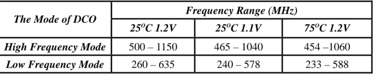
Table 3-1 Frequency Range of DCO with Different Environments ...55
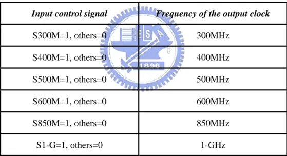
Table 5-1 Frequency of output clock V.S. input control signal...79
Table 5-2 Performance comparison of ADPLL ...93
Chapter 1
Introduction
1.1 Research Motivation
The phase-locked loop (PLL) has been widely used in electronics, communication, and instrumentation today. Examples include memories, microprocessors, hard disk drive electronics, RF and wireless transceivers, and optical fiber receivers. In this section, we show some applications that demonstrate the versatility of phase locking. They are Frequency Multiplication and Synthesis, Skew
Reduction, and Jitter Reduction, separately [1].
Frequency Multiplication A PLL can be modified such that it multiplies its input
frequency by a factor of M. As shown in Fig.1-1, if the output frequency of a PLL is divided by M and applied to the phase detector, we have fout=M‧fin. From another
point of view, since fD= fout /M and fD and fin must be equal in the locked condition, the
PLL multiplies fin by M. The %M circuit is realized as a counter that produces one output pulse for every M input pulses.
Fig.1-1 Frequency multiplication
The frequency-multiplying loop exhibits two interesting properties. First, the PLL provides a multiplication factor exactly equal to M. Second, the output frequency can be varied by changing the divide ratio M, an extremely useful property in synthesizing frequencies.
Frequency Synthesis Some systems require a periodic waveform whose frequency
(a) must be very accurate (e.g., exhibit an error less than 10ppm), and (b) can be varied in very fine steps (e.g., in steps of 30 kHz from 900 MHz to 925 MHz). Commonly encountered in wireless transceivers, such requirements can be met through frequency multiplication by PLLs.
Fig.1-2 shows the architecture of a phase-locked frequency synthesizer. The channel control input is a digital word that varies the value of M. Since fout=M‧fREF , the relative accuracy of fout is equate to that of fREF . For this reason, fREF is derived from a stable, low-noise crystal oscillator. Note that fout varies in steps equal to fREF if
M changes by one each time.
CMOS frequency synthesizers achieving gigahertz output frequency have been reported. Issues such as noise, sidebands, settling speed, frequency range, and power dissipation continue to challenge synthesizer designers.
Skew Reduction The earliest usage of phase locking in digital systems was for
skew reduction. Suppose a synchronous pair of data and clock lines enter a large digital chip as shown in Fig.1-3. Since the clock typically drives a large number of transistors and long interconnects, it is first applied to a large buffer. Thus, the clock distributed on the chip may suffer from substantial skew with respect to the data, an undesirable effect because it reduces the timing budget for on-chip operations.
Now consider the circuit shown in Fig.1-4, where CKin is applied to an on-chip PLL and the buffer is placed inside the loop. Since the PLL guarantees a nominally-zero phase difference between CKin and CKB , the skew is eliminated. From another point of view, the constant phase shift introduced by the buffer is divided by the infinite loop gain of the feedback system. Note that the VCO output,
VVCO , may not be aligned with CKin , a nonetheless unimportant issue because VVCO is not used.
Fig.1-4 Use of a PLL to eliminate skew
Jitter Reduction Many applications must deal with jittery waveforms. Random
binary signals experience jitter because of (a) crosstalk on the chip and in the package (b) package parasitics, (c) additive electronic noise of devices, etc. Such waveforms are typically “retimed” by a low-noise clock so as to reduce the jitter. Illustrated in Fig.1-5(a), the idea is to resample the midpoint of each bit by a D flipflop that is driven by the clock. However, in many applications, the clock may not be available independently. For example, an optical fiber carries only the random date stream, providing no separate clock waveform at the receive end. The circuit of Fig.1-5(a) is therefore modified as shown in Fig.1-5(b), where a “clock recovery circuit” (CRC) produces the clock from the data. Employing phase locking with a relatively narrow
loop bandwidth, the CRC minimizes the effect of the input jitter on the recovered clock.
(a)
(b)
Fig.1-5 (a) Retiming data with D flipflop driven by a low-noise clock
(b) use of a phase-locked clock recovery circuit to generate the clock
Phase locked loop (PLL) based clock generators for microprocessor are often required for on-chip clock generation and multiplication to produce several unrelated clocks with different frequency for other sub-systems. In traditional mixed mode circuit system, PLL is usually implemented in analog building block. Recently, the SoC (system-on-a-chip) architecture has become the underlying architecture for many embedded systems. That means conventional analog PLL integrated with digital circuits is inevitable. Integrating an analog circuit on a die with digital circuits,
however, has a large amount of generated digital noise. Besides, analog PLL is much more sensitive to process variation. It is too hard to use the same analog PLL design in different process [2], [3]. On the other hand, ADPLL are much easier to implement without targeting a specific technology. Their area would also scale down rapidly as the technology shrinks if only active components are used.
Since the implementation of analog component in a digital environment is not a simple task, the linear phase-locked loop (LPLL) and classical digital phase-locked loop (DPLL) which relay on analog component have been replaced by the all digital phase-locked loop (ADPLL) [4]-[7]. The ADPLL becomes more and more popular in recently year. In addition, the ADPLL has characteristics of fast frequency locking, full digitization, and good stability.
1.2 Thesis Organization
This thesis is organized as follows:
Chapter 2 gives an overview of PLL, including LPLL, DPLL and ADPLL, and also
introduces an example of the ADPLL circuit design.
Chapter 3 first introduces the fundamentals of a digitally controlled oscillator (DCO).
The different approaches including several digitally controlled delay elements (DCDE) for DCO design are also addressed. Then, we will focus on the new DCDE design and apply it as fine tune cell to build our DCO. Finally, the detailed description and simulation results of this circuit are given.
(PFD) architecture. Then, the detailed operation flow of the modified PFD will also be addressed. Besides, we also state each function circuit design in the control unit (CU).
Chapter 5 describes the fundamentals of frequency synthesizer and presents the
ADPLL-based frequency synthesizer based on the adjustable counter length mechanism. Finally, we also show the implementation of layout, simulation result, and performance summary.
Chapter 2
An Overview of PLL
In this chapter, we will review three kinds of phase locked-loop circuit, they are Linear PLL (LPLL), Digital PLL (DPLL), and All-Digital PLL (ADPLL), separately [4]. Then, we also introduce a design of the conventional ADPLL circuit, which is proposed by Motorola in 1995 [5].
The first PLL ICs appeared around 1965 and were purely analog devices. In the following years the PLL drifted slowly but steadily into digital territory. The very first digital PLL (DPLL), which appeared around 1970, was in effect a hybrid device. A few years later, the all-digital PLL (ADPLL) was invented. The ADPLL is exclusively built from digital function blocks and hence do not contain any passive components like resistor and capacitors. Different types of PLLs behave differently, roughly, the classifications of PLL circuit are defined as follows:
(1) LPLL (Linear PLL): Each block is analog.
(2) DPLL (Digital PLL): Phase Detector is digital and the others are analog.
(3) ADPLL (All Digital PLL): Each block is digital. The loop filter is from Up/Down
counter. The Voltage Controlled Oscillator (VCO) is from Digital Controlled Oscillator (DCO).
2.1 The Operating Principle of PLL
A PLL is a circuit synchronizing an output signal (generate by an oscillator) with a reference or input signal in frequency as well as in phase. In the synchronized-often called locked-state the phase error between the oscillator’s output signal and the reference signal is zero, or very small. If phase builds up, a control mechanism acts on the oscillator in such a way then the phase error is again reduced to a minimum. In such a control system the phase of the output signal is actually locked to the phase of the reference signal. This is why it is referred to as a phase-locked loop.
The operating principle of the PLL is explained by the example of the linear PLL [4]. In the Figure 2-1, the signals of interest within the PLL circuit are defined as follows:
U1(t): the reference signal
ω1: the angular frequency of the reference signal U2(t): the output signal of the VCO
ω2: the angular frequency of the output signal Ud(t): the output signal of the detector
Uf(t): he output signal of the loop filter
Fig.2-1 Block diagram of PLL
Now we look at the operations of the three functional blocks in the Figure 2-1.
VCO: VCO generate an angular frequency ω2 ,which is determined by the output
signal Uf of the loop filter. The angular frequency ω2 is given by equation (2.1),
whereω0 is the center frequency of the VCO and the K0 is the VCO gain. Equation
(2.1) is plotted graphically in the Figure 2-2.
2= 0+K0 U tf( )
ω ω ⋅ (2.1)
Fig.2-2 The transfer curve of VCO
Phase Detector: the Phase Detector compares the phase of the output signal of VCO with that of the reference signal and generate an output signal Ud(t) which is
equation (2.2), Kd is the gain of the phase detector. Equation (2.2) is plotted
graphically in the Figure 2-3.
d
( )=K
d e
U t ⋅θ (2.2)
Fig.2-3 The transfer curve of PD
Loop Filter: Because the output signal of the PD consists ac component and it is undesired, so we need a loop filter to cancel the ac component.
Different types of PLLs have different building blocks. Following sections will introduce Linear PLL, Digital PLL and All Digital PLL The next section will discuss the design of Linear PLL.
2.2 Linear PLL
Although the PLL is a non-linear system, it can be described with a linear model if the loop is in lock [8]. When the loop is in lock the phase error signal generates by the phase detector settles on a constant value. In the locked state, the output signal has a fixed frequency as the input reference signal. A phase difference between the input
reference signal and output signal may exist depending on the type of PLL used. When the loop is in lock the phase difference remains constant. The Linear PLL is built from three purely analog function blocks. They are Phase Detector, Loop Filter and VCO .The three blocks are describe in the following:
Phase Detector: Phase Detector can be a four phase analog multiplier or analog signal mixer.
Loop Filter: Loop Filter is a passive or active RC filter, it filter high frequency signal and noise from phase detector and environment. The output of the filter is a DC value to send to VCO.
VCO: It is a ring oscillator which construct by inverters. The frequency is controlled by the dc value from Phase Detector.
Fig.2-4 Linear PLL model
The building blocks of Figure 2-4 are taken as basis for the mathematical model of a Linear PLL in lock. From the model, we can derive the transfer function of the
Linear PLL: ( ) ( ) ( ) ( ) ( ) out PD VCO ref PD VCO K K F s s H s s s K K F s θ θ = = + (2.3)
The phase error transfer function is equal to the following:
( ) ( ) ( ) ( ) e ref PD VCO s s H s s s K K F s θ θ = = + (2.4)
The VCO control voltage transfer function is equal to the following:
( ) ( ) ( ) ( ) ( ) C PD ref PD VCO V s sK F s H s V s s K K F s = = + (2.5)
The following observation is made from the transfer function give in equation (2.3), (2.4) and (2.5). At first, we discuss the Linear PLL transfer function, give in equation (2.3), it has a low-pass characteristic. This means that for slow (low frequency) variations in the reference phase, the loop will basically track the input signal and produce an output phase.
The phase error transfer function, give in equation (2.4), has a high pass characteristic. This implies that for slow variations in the reference phase, the phase error will be small. However, fast variations in the reference phase will not be filtered and show up as a phase error.
The VCO control voltage transfer function, give in equation (2.5), also has a high pass characteristic. However, depending on the parameter of the loop filter, it can take on a more band-pass shape.
The linear model in Figure 2-4 enables us to analyze the tracking performance of the Linear PLL, i.e., the system maintains phase tracking when excited by phase steps, frequency steps, or other excitation signals. So we can analyze the characteristic and the responses of the Linear PLL in S-domain, and then, calculate all parameter to design a Linear PLL to satisfy the specification.
2.3 Digital PLL
In this section, we will describe the operating principle and circuit design of Digital PLL [4]. Figure 2-5 shows the Digital PLL which consists digital Phase Frequency Detector, analog Charge Pump, analog Loop Filter, analog Voltage Controlled Oscillator and Frequency Divider.
The Phase Frequency Detector can detect the phase and frequency error between the input reference signal and feedback clock signal. The output of the PFD is up signal or down signal. The up signal and down signal control the Charge Pump to charge or discharge. Loop Filter can filter the high frequency signal. Loop Filter outputs a low frequency signal to control the VCO. By including a Frequency Divider in the feedback path, the VCO output clock runs N times faster than the feedback clock. The next sections will describe the circuit and behavior of the PFD, CP, LF, FD, and VCO.
PFD Charge Pump Loop Filter VCO Frequency Divider reference clock up down feedback clock
Fig.2-5 Digital PLL Block
2.3.1 Phase Frequency Detector
This section will describe the operation and implementation of the PFD circuit. Figure 2-6 shows an example of the PFD circuit and Figure 2-7 shows the waveforms in some conditions. Unlike multipliers and XOR gate, sequential PFD generates two outputs that are not complementary. Illustrated in Figure 2-6, the operation of a typical PFD is as follows.
When the feedback clock is high and the input reference is low, then the PFD produces positive pulses at down signal, while up signal remains at zero. Conversely, if input reference is high and feedback clock is low then positive pulses appear at up signal while down signal is zero. It should be note that, in principle, up and down are never high together in the simulation. The average value of up – down is an indication of the frequency or phase difference between input reference and feedback clock.
Fig.2-6 Phase Frequency Detector Block
(a)
(b)
Fig.2-7 (a) PFD response with input reference lagging feedback clock
Fig.2-8 PFD state diagram
In the Figure 2-8, it shows the PFD circuit behavior. It has three state diagrams: up=1,down =0(state I ) ; up=0,down=0(state 0 ) ; up=0,down=1(state II ). Because the PFD is buildup from two edge-triggered sequential circuits, we can avoid dependence of the output upon the duty cycle of the inputs.
If the PFD is in the state 0, up=down=0, then a transition on A take it to state I, where up=1, down=0. With state I is reached, any more rising edges at input A won’t cause state change at all. The circuit will remain in this state until a transition occurs on B, upon which the PFD returns to state 0. The switching sequence between state 0 and state II is similar.
The PFD can nominally detect a full range of phase difference, i.e. +2π, -2π. A phase difference larger than 2π is truncated with respect to integer of 2π. The output of the PFD can drive a three-state charge pump. The charge pump and loop filter will be discussed followed.
2.3.2 Charge Pump/Loop Filter
In a PLL system, the charge pump transfers the digital signal of up and down from the PFD to an analog signal. Figure 2-9 shows a simple model of the charge pump circuit. It consists of both matched current sources, each with a fixed value. When the up signal is high, the switch connects to A and Vc is charged by the up current source Iup. Similarly, when the down signal is high, the switch connects to B
and Vc is charged by the lower current source Idown. If both up signal and down signal
are low, then the switch maintains at original node and Vc holds the original voltage. Most of the PLL’s specifications are determined by the loop filter. The loop filter can be either passive or active. In general, a passive filter is simple to design and has better noise performance. The passive filter was shown in Figure 2-10, which may be first-order, second-order, or other high order structures.
(a) (b) (c)
Fig.2-10 three kinds of passive Loop Filter
Fig.2-11 The response of PFD and Charge Pump/Loop Filter
As show in Figure 2-11, charge pump circuit convert the logic state of the PFD (Up and Down) into an analog counterpart for controlling the VCO. The charge pump output and the input of a VCO must have the low leakage tendency. So a passive loop filter shapes the output of the charge pump circuit to suppress the un-wanted message. The time domain response can be shown in Figure 2-11.
As discussed in the previous section, if the input reference signal leads the feedback signal, the pulse appear at up signal, then positive charge accumulates on capacitor steadily. Conversely, if the input reference signal lags the feedback signal, the charge is removed from capacitor on every phase comparison. In the third state, when input reference and feedback signal are equal, up and down keep low. Both switches are off, and the output signal Vc remains constant.
The above discussions of the Figure 2-11 only use a capacitor as the loop filter. But this kind of filter makes the PLL unstable. We can use the loop filter which was shown in Figure 2-10(b), Figure 2-10(c) to avoid instability.
2.3.3 Voltage Controlled Oscillator
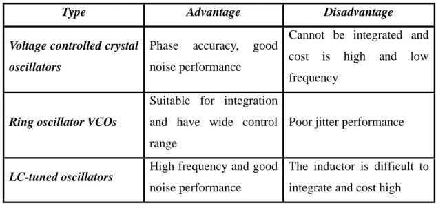
In this section, we will describe the voltage-controlled oscillator which is the critical circuit in the PLL. The input voltage of the VCO generated from the loop filter and the output frequency signal of VCO is controlled by the input voltage. In some oscillators, the frequency of the oscillator is controlled by a current rather then a voltage. They are referred as current-controlled oscillators (CCO) and play the same role as those of VCOs in PLLs. The VCO and CCO are similar. Of course, there are various types of VCO than can be used in PLLs.
The Table 2-1 show three various types of VCO. Basically, the VCO has to fulfill some constraints is the phase noise in the frequency domain or the timing jitter in the time domain. Other important factors are the bandwidth of the VCO, linearity of the controlled voltage, output voltage swing and the power consumption [9][10][11].
Table 2-1 Comparison of different type oscillators
Type Advantage Disadvantage
Voltage controlled crystal oscillators
Phase accuracy, good noise performance
Cannot be integrated and cost is high and low frequency
Ring oscillator VCOs
Suitable for integration and have wide control range
Poor jitter performance
LC-tuned oscillators High frequency and good
noise performance
The inductor is difficult to integrate and cost high
Some of the most important considerations of VCO are: [12]
(1) Phase Stability:
The frequency spectrum of a VCO output should look likes an ideal impulse, i.e., the phase noise of a VCO must be as low as possible.
(2) Electrical Tuning Range:
The tunable frequency range of a VCO must be able to cover the entire required frequency range of the interested application.
(3) Tuning Linearity:
An ideal VCO has a constant gain at the entire frequency range. Also, a constant VCO gain can simplifies the design procedure of a VCO.
(4) Power Supply Sensitivity:
Since there are many digital circuits in a modern transceiver circuit, the switching activities of digital circuits will somewhat influence the power supply of the whole system. The switching noise induced by digital circuits will also couple to the power
supply of the VCO and influence its output waveform. Therefore, in VCO the dependency of the oscillating frequency on the power supply must be as low as possible.
(5) Frequency pushing:
The dependency of the center frequency on the power supply voltage.
(6) Frequency pulling:
The dependency of the center frequency on the output load impendence.
(7) Low cost, Phase noise, DC consumption current, Harmonic/spurious
In the next, we will show an LC-Tank VCO and a ring oscillator in the Figure 2-12 and Figure 2-13 [11]. In the LC-Tank VCO, the oscillation conditions are already shown in [11], its operation frequency is 0 1
L C
ω = . Where RP is the parasitic
resistance in parallel to the LC-tank, and RL and RC are the parasitic resistances of L
and C, respectively.
Fig.2-13 five stage signal ended ring oscillator
The second type oscillator is ring oscillator as shown in Figure 2-13 has been widely used in PLL for application of clock recovery and clock generation before, it can be smoothly integrated in a standard CMOS process without taking extra processing steps because it dose not require any passive resonant element.
When the ring oscillator is employed as a voltage controlled oscillator, the desired wide operating frequency range can be easily obtained. Different output frequency is achieved by adjusting the timing delay of each stage in the ring oscillator.
The other category of oscillator is to eliminate that the real part of the loop’s impedance so that the poles are pure imaginary. The LC-tank VCO is a typical resonator oscillator that bases on the idea and is called resonator oscillator. The VCO is the most challenging part of the PLL and we have to design carefully.
2.3.4 Frequency Divider
In some application, we need a high frequency clock generator and the crystal-oscillator is not satisfied, because the frequency of the crystal-oscillator is too
small. Therefore, the multiple-frequency-technology that utilizes PLL is presented. For example, if the divider module is four, then the output frequency of VCO is a four times of the input reference signal’s frequency. The Figure 2-14 shows an example of divider, which uses a true single-phase clocking (TSPC) register. If we need higher division, it can be achieved by simple cascading divide-by-2 stages. The next is the advantages and the disadvantages of the divider:
Advantages:
(1) Reasonably fast
(2) No static power consumption (3) Compact size
(4) Differential clock not require
Disadvantages:
(1) Slowed down by stacked PMOS, signals goes through three gates per cycle (2) Requires full swing input clock signal
2.4 All Digital PLL
In this section we will describe All Digital PLL, which has characteristics of fast frequency locking, full digitization and good stability. Because of the availability of low-cost ADPLL ICs, this type of PLL can replace the classical DPLL in many applications today. The ADPLL is made as a digital building block, it dose not contain any passive component, such as resistors and capacitors.
The ADPLL consists of a digital phase frequency detector (PFD), a control unit, a frequency divider, and digital control oscillator (DCO) as shown in Figure 2-15. All signals in the ADPLL are digital signals. The PFD detects the frequency difference and the phase difference between the input reference signal and the feedback signal. The control unit receives the signal, produced by the PFD, and produces a set of digitally controlled signals to control the DCO.
By including a divide-by-N divider in the feedback path, the DCO output frequency runs N times faster than input reference signal. The divide-by-N divider is an optional component in the ADPLL. The functional blocks of the ADPLL imitate the function of the corresponding analog blocks. Because the ADPLL consists of digital circuits entirely, there are many different of design methods to achieve the functions of them.
Fig.2-15 All Digital Phase-Locked Loop
The ADPLL system is a discrete-time system, hence analyzing the ADPLL in s-domain is not suitable. Although it is possible to take an entire PLL-description and then transform it from s-domain into z-domain, this is unnecessary difficult. Instead, one transforms each component into z-domain and then proceeds with the analysis in z-domain. The ADPLL is best described in z-domain.
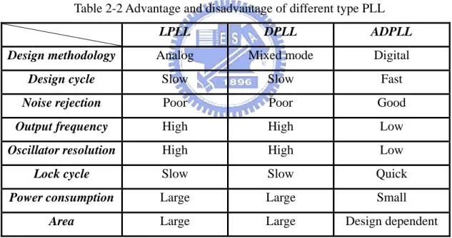
In the Linear PLL, Digital PLL and All Digital PLL, they have many advantages and disadvantages respectively. We summarize them in Table 2-2. As shown in the Table 2-2, we can know that they use different design methodology, because the ADPLL is a digital circuit design so it can be designed by standard cell library. Hence the ADPLL just need a short design cycle than the analog architecture.
The ADPLL also has higher noise immunity than LPLL and DPLL. The VCO of the LPLL or the DPLL produces a continuous frequency band but the DCO of the ADPLL produces a discrete frequency band, so the VCO has higher resolution than DCO. In general, the ADPLL have a less power consumption than analog architecture because of using digital circuits. Besides, since the loop filter of LPLL or DPLL has one or more large capacitors, whose area can not be efficiently reduced as the process technology improving. In addition, the ADPLL can shorten lock time by dealing with
digital signal.
The design of PLL is a trade-off between jitter performance, frequency resolution, phase resolution, lock-in time, area cost, power consumption, circuit complexity and design cycle. It is hard to design one PLL suitable for all applications. For fast-locking frequency synthesizer applications, such as a frequency hopping multiple access system, the lock-in time is the most critical design issue. And for portable or mobile applications, lock-in time is also very important since the PLL must support fast entry and exit from power management techniques.
Table 2-2 Advantage and disadvantage of different type PLL
LPLL DPLL ADPLL
Design methodology Analog Mixed mode Digital
Design cycle Slow Slow Fast
Noise rejection Poor Poor Good
Output frequency High High Low
Oscillator resolution High High Low
Lock cycle Slow Slow Quick
Power consumption Large Large Small
Area Large Large Design dependent
In traditional analog PLL designs, fast acquisition requires tuning of the VCO free-running frequency near the desired the frequency in advance or to increase loop bandwidth. But increasing the loop bandwidth degrades jitter performance, and the extra VCO tuning range is not easy to be achieved since there always has process variations, voltage variations, and temperate variations (PVT variations). Some
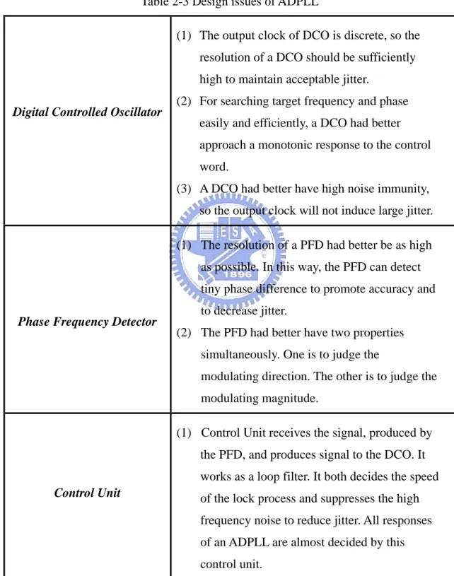
critical issues in ADPLL design are listed in the following table.
Table 2-3 Design issues of ADPLL
Digital Controlled Oscillator
(1) The output clock of DCO is discrete, so the resolution of a DCO should be sufficiently high to maintain acceptable jitter.
(2) For searching target frequency and phase easily and efficiently, a DCO had better approach a monotonic response to the control word.
(3) A DCO had better have high noise immunity, so the output clock will not induce large jitter.
Phase Frequency Detector
(1) The resolution of a PFD had better be as high as possible. In this way, the PFD can detect tiny phase difference to promote accuracy and to decrease jitter.
(2) The PFD had better have two properties simultaneously. One is to judge the
modulating direction. The other is to judge the modulating magnitude.
Control Unit
(1) Control Unit receives the signal, produced by the PFD, and produces signal to the DCO. It works as a loop filter. It both decides the speed of the lock process and suppresses the high frequency noise to reduce jitter. All responses of an ADPLL are almost decided by this control unit.
2.5 An Example of The Conventional ADPLL Design
In this section, we will introduce a design of the conventional ADPLL, which is proposed by Motorola in 1995 [5]. It has a 50-cycle phase lock, has a gain mechanism independent of process, voltage, and temperate, and is immune to input jitter. A DCO forms the core of the ADPLL and operates from 50 to 500 MHz, running at 4X the reference clock frequency. The DCO has 16b of binary weighted control and achieves LSB resolution under 500fs.
2.5.1 Architecture Overview
The ADPLL uses four loosely coupled modes of operation: frequency acquisition, phase acquisition, phase maintenance, and frequency maintenance. The phase-lock process is separated into frequency acquisition and phase acquisition, which significantly reduces the phase-lock time penalty.
Fig. 2-16 depicts a block diagram of the ADPLL. The DCO control register holds the 16 b, binary weighted DCO control word, which dictates the frequency of the DCO. Arithmetically incrementing or decrementing the DCO control word modulates DCO frequency and phase. The adder and subtracter provide the updates to the DCO control register. Also, the anchor circuit, which contains a register and an adder, updates the DCO control register in frequency maintenance mode. The frequency-gain register and phase-gain register provide operands to the adder and subtractor via the add mux and subtract mux. In addition, the phase-gain register provides data to the
anchor circuit. The control block marshals these sub-blocks to implement the different ADPLL modes of operation.
Fig.2-16 The Conventional ADPLL Block Diagram
Phase lock begins with frequency acquisition. In this mode an algorithm sweeps the DCO frequency range (divided by 4) to match that of the reference clock. The algorithm makes incremental changes to the DCO control word based on the output of the frequency comparator. The value held in the frequency-gain register determines the magnitude of the incremental changes. At the end of frequency acquisition, the ADPLL transfers the DCO control word defining the correct (baseline) frequency to the anchor register.
When frequency acquisition is complete, the ADPLL enters phase acquisition mode. During phase acquisition, the ADPLL increments or decrements the DCO
control word until the phase detector senses a change in the phase polarity of the reference clock relative to the internal clock. The value held by the phase-gain register dictates the magnitude of the changes to the DCO control word in phase acquisition mode, as well as in phase and frequency maintenance modes. Phase acquisition is finished when a change in phase polarity occurs. To complete the phase-lock process, the anchor register transfers its contents to the DCO control register, restoring the DCO control word value representing the baseline frequency.
After the phase-lock process, frequency maintenance and phase maintenance will operate concurrently. In frequency maintenance mode, an algorithm increments or decrements the content of the anchor register, changing the baseline frequency value. In phase maintenance mode, the ADPLL increments or decrements the DCO control word every reference cycle, based on the output of the phase detector, unless the polarity of phase error changes from that of the prior cycle. When phase polarity changes, the anchor register transfers its contents to the DCO control register to restore the baseline frequency. The ADPLL varies the magnitude of changes to the DCO control word, which changes the ADPLL response from overdamped to underdamped and vice versa as necessary.
2.5.2 Digitally Controlled Oscillator
At the heart of the ADPLL is a digitally-controlled oscillator (DCO). The ADPLL controls the DCO frequency through the DCO control word, the output of a
number of inverting stages in the DCO is obtained by using one enabling NAND gate and eight controllable cells. A mux selects between using four of the controllable DCO cells rather than eight to increase the range of the DCO. This selection occurs based on the first frequency comparison at the beginning of phase lock. Figure 2-17(a) illustrates the constituent DCO cell. The sizing ratio of the control devices is 2x, achieving binary weighted control. The most significant control-word bit (15) corresponds to the largest control device.
A key design criterion in DCO circuit design is to provide sufficient control word resolution to maintain acceptable jitter. With a minimum device width of 1.2 um and a maximum of 256 x 1.2 um, the DCO can achieve 9 b of control in each of 8 cells. Besides, using a stand-alone, minimum width PMOS device (and eliminating the corresponding pull-down device) adds a further bit of resolution in each cell. Taking the same PMOS device and using it in only 4 of 8 DCO cells adds yet another bit of resolution.
Fig. 2-17(b) depicts this concept, showing the DCO where control bit 5 affects four DCO cells and higher order bits affect eight DCO cells. Similarly, two more bits of resolution result from using the same PMOS device in only 2 of 8 and 1 of 8 DCO cells respectively. Finally, using the same width PMOS device but increasing the channel length-each used in only 1 of 8 cells-results in three more bits of resolution. Empirically tuning these devices compensates for the increase in channel-to-gate capacitance associated with longer lengths. Overall, these techniques yield 16 b of resolution.
(a)
ENABLE DCO_control [5]
DCO_control [15:6]
(b)
2.5.3 Frequency Acquisition
The goal of frequency acquisition mode is to lock the DCO frequency (div4) to that of the reference clock frequency, ignoring phase alignment. A modified binary-search algorithm sweeps the DCO frequency range in progressively smaller increments. The implementation of this algorithm centers around a frequency-gain register and a frequency comparator.
The frequency-acquisition algorithm begins with initializing the DCO control register and the frequency gain register. A frequency comparator then performs the first frequency comparison of the DCO output frequency relative to the reference clock frequency. By default, a mux selects the 8-cell DCO configuration. However, if the first comparison indicates the DCO frequency is slow, then the mux selects the 4-cell DCO. The comparator then performs the next frequency comparison. Based on the results of the comparison, the adder or subtracter increments or decrements, respectively, the DCO control register by the value in the frequency gain register.
If the comparator output changes from fast to slow (or vice versa) over two consecutive frequency comparisons, then a change in search direction has occurred. The algorithm reduces frequency gain on every change in search direction. The algorithm proceeds with successive frequency comparisons until the frequency gain falls below the value of the DCO control word shifted right by ten places. Finally, the algorithm loads the anchor register with the DCO control word value matching the baseline frequency.
In implementing the frequency comparison technique of the algorithm, a comparator accepts as inputs the reference clock and the DCO output. It generates two mutually exclusive output signals, “slow” and “fast,” and also an enable signal for the
DCO. The comparator uses the reference clock edge to assert the DCO enable, forcing initial phase alignment of the DCO output edge to the reference clock edge. The comparator takes one-half reference cycle for synchronization before asserting “slow” or “fast.” Resetting the comparator to disable the DCO requires the remainder of the reference cycle. Hence, a complete frequency-comparison iteration takes two reference cycles.
For example, Fig. 2-18 shows a block diagram of the frequency comparator and Fig. 2-19 shows a timing diagram of two frequency comparison iterations. The first rising edge of the reference clock enables the DCO at A, and the second rising edge captures the output of a 4-b counter at B, the input to the synchronizer. If this signal at
B is asserted when the second rising reference edge arrives at the synchronizer, then the DCO is fast. Conversely, if the signal at B is not asserted when the second rising reference edge arrives at the synchronizer, then the DCO is slow.
After synchronization, the comparator outputs a “fast” or “slow” at C. Concurrently, the comparator disables the DCO at D, and the ADPLL loads the new control word. The circuit at E matches (via circuit replication) the delay inherent in enabling the DCO and the delay inherent in the DCO pulse counter. If the frequency of the DCO (div4) identically matches the frequency of the reference clock, then both the signal and the synchronizer clock arrive simultaneously at the synchronizer (B) with the same rise times.
In implementing the gain strategy of the algorithm, an adder and subtracter receive both the value of a frequency-gain register (via the add and subtract muxes) and the DCO control word. Shifting the frequency-gain register once to the right
only the odd bits of the frequency-gain register (the add gain), and the subtract mux receives only the even bits of the frequency-gain register (the subtract gain). In addition, setting the two most significant bits of the frequency-gain register initializes the add gain to 400016, and the subtract gain to 200016.
Now that the DCO frequency is locked to that of the reference clock, the DCO enable remains asserted so that the DCO is in the free-running state, ready for phase-acquisition.
Fig.2-19 Frequency Comparator Timing
2.5.4 Phase Acquisition
The goal of this mode is to align the DCO clock edge to the reference clock edge. Because, in practice, there are several stages of logic separating the DCO clock from the DCO output. The implementation of this algorithm centers around a phase detector and a phase-gain register.
The phase-acquisition algorithm begins by selecting the phase gain and deselecting the frequency gain via the add and subtract muxes. The phase detector asserts a digital signal, either "ahead" or "behind," based on the relation of the DCO clock edge to the reference clock edge. This event increments or decrements the DCO control word by the value in the phase-gain register, thereby modulating the DCO phase relation.
versa on successive cycles, phase acquisition is complete, and the ADPLL transfers the anchor register contents to the DCO control register, restoring the baseline frequency and completing phase lock.
(a) (b)
Fig.2-20 (a) Phase Acquisition Mux, (b) Phase Acquisition Resolved
There exists a pathological phase-acquisition scenario with this implementation where the false detection of a change in phase polarity can occur. The scenario arises when the initial phase error between the DCO clock and the reference clock is 180 degrees. As shown in Fig. 2-20(a), inserting a divide-by-two circuit between the DCO clock and phase detector can preclude this scenario. In addition, Fig. 2-20(b) depict a timing diagram of the resulting circuit. The mux selects the divide-by-one circuit after phase acquisition is complete, constraining phase alignment to a rising DCO clock edge.
2.5.5 Phase and Frequency Maintenance
Once the phase lock process completes, a maintenance mode begins. The ADPLL decouples this mode into phase maintenance mode and frequency maintenance mode. Phase maintenance strives to preserve the phase alignment of the DCO clock relative to the reference clock, while frequency maintenance strives to preserve the analogous match in frequency.
In phase maintenance, the ADPLL increments or decrements the DCO control word every reference cycle, based on the output of the phase detector, unless it discerns a change in phase polarity from that of the prior cycle. The value held in the phase-gain register dictates the magnitude of the changes to the DCO control word. Whenever a change in phase polarity occurs, the ADPLL transfers the anchor register contents to the DCO control register, restoring the baseline frequency.
However, reference-clock frequency drift or DCO frequency drift induced by voltage or temperature variations requires that the ADPLL has the capability of changing the baseline frequency. Frequency maintenance mode provides such means by updating the anchor register.
Chapter 3
Digitally Controlled Oscillator
Digitally controlled oscillator (DCO) is the key component of ADPLL. Like most voltage controlled oscillators (VCO), DCO consists of a frequency-control mechanism with an oscillator block. In this chapter, first, we will introduce the basic concepts and approaches, as well as some examples in DCO circuit design. Finally, the proposed DCO circuit design in our ADPLL will be presented.
3.1 Basic Concepts of DCO
The basic transfer function of DCO is as follows [22]:
fDCO( )D = f d( n−12n−1+dn−12n−1+⋅⋅⋅+d121+d02 )0 (3.1) The output wave of DCO, typically in the form of square wave, which has a oscillation frequency of fDCO that is a function of a digital input D. The DCO transfer
function is usually defined so that the frequency fDCO is changed linearly with its input
word (D), hence it is also typically expressed as:
fDCO( )D = foffset+ ⋅Δ (3.2) D f where foffset is a constant offset frequency and Δf is its frequency quantization step.
of the quantized digital input D, the transfer characteristic of DCO is evidently discontinuous. In other words, as shown in equation 3.2, this will result in a finite frequency step size Δf and hence set some fundamental limits on the achievable jitter of the ADPLL. For this reason, it is the most important that the resolution of DCO have to be sufficiently high to maintain acceptable jitter. Besides, there are still some important issues on DCO design, such as: the DCO had better approach a monotonic response to the DCO control word and own high noise immunity at the same time, so the output clock will not induce larger jitter.
3.2 Different Approaches for DCO design
As shown in Fig. 3-1, a straightforward idea to implement DCO in [19] is utilized a digital-to-analog converter (DAC) and a conventional voltage controlled oscillator (VCO). However, it is very difficult to design a high resolution DAC and the area cost will be very high due to the DAC and VCO. Besides, the VCO is an analog block making it easily be influence by power and substrate noise.
A high frequency oscillator with a program frequency divider is commonly used for another type of DCO. As shown in Fig. 3-2, the program divider receives an n-bit digital control word D which indicates the divide ratios. The DCO output clock is to be divided from a high frequency oscillator. In this arrangement, however, the DCO output frequency resolution is limited by the high frequency oscillator. In other words, this operation will require the oscillator operating at a very high frequency and hence consume much power dissipation.
Fig.3-2 DCO composed of a high frequency oscillator and a divider
Because of the limitation on speed, directly synthesis a signal rather than dividing from a high frequency oscillator is often used in the conventional DCO. For this reason, the ring oscillator-based DCO has thus been used commonly in ADPLL for many applications today. Therefore, we will focus on the ring oscillator-based DCO design in the following.
So far, there are two main parameters to modulate the frequency of the ring oscillator. One is the total number of the delay elements, usually taken for the coarse tune method, and the other is the propagation delay time of the delay elements (i.e.
inverters), which is usually taken for the fine tune method. The first frequency modulating parameter is usually realized by a path-selection approach, and Fig. 3-3 shows the example [22]. In this example, 2n delay buffer are connected in series. A decoder decodes an n-bit control word D into 2n control lines. Hence, if the propagation delay time of each buffer stage is Tbuffer, then the time resolution is
2‧Tbuffer.
Fig.3-3 DCO realized by a path-selection method
The second frequency modulating parameter is usually realized by a digitally controlled delay element (DCDE). Moreover, we use a new DCDE in the DCO design and it has features of its monotonicity and insensitivity to PVT variations. In the following section, we will introduce several kinds of DCDE and the new DCDE circuit design.
3.3 Digitally Controlled Delay Element
There are several different architectures that have been used to implement a digitally controlled delay element (DCDE). However, they can generally be classified into the parallel-inverter-based and the single-inverter-based delay elements, individually. First, we take the parallel-inverter-based DCDEs into consideration, which are summarized in [22].
One simple DCO consists of a bank of tri-state inverter buffers was proposed in [3], [20], [21], as shown in Fig. 3-4. By enabling the numbers of tri-state inverter buffers, we can control the resolution of DCO. It is simple and easy to implement; however, it needs large area and high power dissipation for the fine tune necessarily in the DCO design. Besides, the resolution is hard to be uniform.
The other example, as shown in Fig. 3-5, a DCO is implemented by an add-or-inverter (AOI) cell and or-and-inverter (OAI) cell with two parallel tri-state inverters was proposed in [23]. The basic method is to adjust the driving capability with resistance control. The advantage is that this fine tune method of DCO cell has less area and power dissipation compared with [3], [20], [21]. However, since it’s based on AOI-OAI cell to change the delay resolution, the resolution step is also hard to be uniform and sensitive to power-supply variation. Besides, is also requires an additional decoder for mapping the control input of AOI-OAI cell.
OAI AOI EN1 1 EN2 1 OUT A1 B1 A2 B2
Fig.3-5 DCDE composed of an AOI-OAI
Moreover, we will keep on discussing the single-inverter-based DCDEs. Within most of the architectures, usually, a switch network of nMOS transistors is placed at the source of the nMOS transistor in a CMOS inverter, as shown in Fig. 3-6. In this circuit only the delay of the falling edge of the output voltage can be controlled by the
switch network of pMOS transistors should be placed at the source of the pMOS transistor (M2) in the inverter.
Fig.3-6 Basic structure of a delay element
The number of nMOS transistors in the switch network depends on the desired number of different separate delays and the required delay resolution. Depending upon the digital input vector, the equivalent resistor of the switch network (or the current passing through it) changes and causes the delay of the inverter to change [5], [13].
One of the main drawbacks of these delay elements is that the delay of the circuit may not change monotonically with respect to the input vector. It makes the design of the circuit more difficult, hence the circuit should be thoroughly simulated for all the possible combinations of the input vector. For example, in the case of the circuit used in [13], finding the sizes of the transistors in the switching network is a matter of optimal coding.
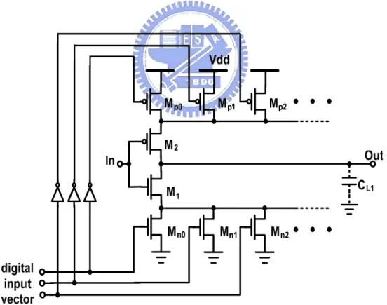
Fig. 3-7 illustrates a DCDE based on the current-starved inverter. The charging and discharging currents of the output capacitance (CL1) of the inverter, composed of
M1 and M2, are controlled by two sets of current-controlling nMOS (Mn0, Mn1, … )
and pMOS (Mp0, Mp1, … ) transistors at the source of M1 and M2, respectively. The
current controlling transistors are sized in a binary fashion. It allows us to achieve binary incremental delays. As can be seen, by applying a specific binary vector to the controlling transistors, a combination of transistors is turned on at the sources of M1
and M2 transistors. Such an arrangement controls the rise time and fall time, and hence
the delay, of the output voltage of the inverter.
Fig. 3-8 illustrates another technique for implementing a DCDE. In this circuit, a variable resistor is used to control the delay. A stack of n rows by m columns of nMOS transistors is used to make the variable resistor. This resistor subsequently controls the delay of M1. In the circuit of Fig. 3-8, only the falling edge of the Out can
be changed with the input vector. Similarly, another stack of pMOS transistors can be used at the source of the pMOS transistor, M2, to have control over the delay of the
rising edge.
Fig.3-8 Another delay element
One of the problems with the above mentioned single-inverter-based DCDE architectures is the nonmonotonic delay behavior with ascending binary input pattern. As can be seen in the circuits of Figs. 3-7 and 3-8, the input vector changes the effective resistance of transistor(s) placed at the source of the nMOS or pMOS transistors of the inverter. This not only changes the resistance at the source of M1 or
M2, but also changes the parasitic capacitance associated with transistors at these
nodes. This is because the parasitic capacitance at the drain of a MOSFET is different in the ON and OFF states. Therefore, there are two factors depending on the input vector to affect the delay:
(1) The resistance of the controlling transistors:
The circuit delay can be increased/decreased by increasing/decreasing the effective ON resistance of the controlling transistors at the source of M1 (M2).
(2) The effective parasitic capacitance of the controlling transistors:
As the effect capacitance of the controlling transistors at the source of M1 (M2)
increases due to the input vector, the charge sharing effect causes the capacitance at the output of the current-starved inverter to be (dis)charged faster and the overall delay of the circuit decreases.
Because the W/L ratio of the controlling transistors have to change in binary fashion, usually, the channel length L, is thus increased to realize a small W/L ratio. A longer transistor puts a higher resistance and a lager parasitic capacitance at the source of M1 (M2). A larger resistance increases the delay; however, a larger parasitic
capacitance decreases the delay. Therefore, it may make monotonic characteristic of the DCDE can not be ensured with ascending input vector. This situation will be further complicated as the number of delay controlling transistors increases.
For this reason, it becomes difficult to predict the circuit delay for a given input vector and will cause the circuit to be simulated for all the possible input combinations during the design phase. The design of high-resolution delay element becomes a nontrivial task due to the lack of a one-to-one relationship between
not met, it is not very clear whether the size of a transistor in the nMOS or pMOS network should be increased or decreased.
A new architecture, which eliminates the above-mentioned non-monotonic delay behavior, is proposed in [14]. Fig. 3-9 shows the new delay element. As can be seen in this figure, the delay of a current-starved inverter, M8 – M11, is controlled by the
current passing through M8 and M11. Transistor M8 controls the fall time of the output
of this inverter while M11 controls the rise time. The current passing through M8 is
determined by M5 and the current passing through M5. Meanwhile, the current passing
though M11 is determined by transistors M5 – M7 and the current passing through M5.
Fig.3-9 New DCDE architecture
The delay controlling pMOS transistors M1, M2, M3,… should be sized in a
binary fashion. The input vector turns these pMOS transistors on or off. In this way, the current passing through M5 will be determined by the input vector. This
controlling current will later be mirrored to M8 and M11, and controls the delay of the
inverter. Note that transistor Mp is always on. This circuit can implement 2N different
delays where N is the number of pMOS controlling transistors. Note that the parasitic capacitances at the source of M9 and M10 are the same for all the input vector
combinations.
Therefore, when the input vector changes, only the (dis)charging current of the inverter changes, and the charge sharing remains the same. This causes the delay of the circuit to change monotonically with respect to the input vector, which makes the design of this circuit straightforward compared to the other delay elements.
Another point which is worth mentioning is that both the rising and falling edge delays can be varied by this circuit. This has come at the expense of three more transistors (M6, M7, and M11), while in the conventional delay elements, the number of
added transistors for this purpose is more. Note that transistors M6, M7, and M11 do not
need to be very large, while the delay-controlling transistors in conventional delay elements are large and consume extra area due to their binary sizing scheme.
The design procedures of the new DCDE are explained as follows [15]:
(1) Transistor M8 / M11 should be much smaller than M9 / M10 such that the
discharging current is controlled by M8 / M11. The ratio of transistors M10 and M9
should be μn /μp where μn and μp represent electron and hole mobilities. Transistor
(M5, M6) / M7 can be the same size as M8 / M11, since these transistors make the
current mirrors. However, these transistors may have different sizes to reduce the static power consumption of the DCDE, as explained in [14].
(2) The number of pMOS controlling transistors (N) can be obtained from the desired