Improvement of TDDB reliability, characteristics of HfO
2
high-k/metal gate
MOSFET device with oxygen post deposition annealing
Chia-Wei Hsu
a, Yean-Kuen Fang
a,*, Wen-Kuan Yeh
b, Chun-Yu Chen
a, Yen-Ting Chiang
a, Feng-Renn Juang
a,
Chien-Ting Lin
c, Chien-Ming Lai
ca
VLSI Technology Laboratory, Institute of Microelectronics, Department of Electrical Engineering, National Cheng Kung University, Tainan, Taiwan 701, Taiwan
bDepartment of Electrical Engineering, National University of Kaohsiung, No. 700, Kaohsiung University Rd., Nanzih District, Kaohsiung, Taiwan c
Central R&D Division, United Microelectronics Corporation (UMC), No. 3, Li-Hsin Rd. II, Hsin-Chu City, Taiwan 300, Taiwan
a r t i c l e
i n f o
Article history:
Received 23 November 2009
Received in revised form 21 January 2010 Available online 1 March 2010
a b s t r a c t
In this work, influences of oxygen effect on an Hf-based high-k gate dielectric were investigated. A post deposition annealing (PDA) including oxygen ion after high-k dielectric deposition was used to improve reliability of the Hf-based high-k/metal gate device. The basic electrical characteristics of devices were compared with and without the PDA process. Experiment results show that the oxygen PDA did not degrade the drive current and effective oxide thickness of the Hf-based gate devices. In addition, reliabil-ity issues such as positive bias instabilreliabil-ity, negative bias instabilreliabil-ity and TDDB were also improved by the oxygen PDA significantly. During the TDDB test, the charge trapping was characterized by an in situ charge pumping system, which could make us to understand the variations of interface trap during the reliability stress easily.
Ó 2010 Elsevier Ltd. All rights reserved.
1. Introduction
Hf-based dielectrics are considered as the leading high-k candi-dates with metal electrode for next generation of CMOS technology
[1]. However, compared to the silicon oxide (SiO2), the Hf-based
dielectrics have a higher concentration of defects[2,3]. These de-fects play the role of charge trapping source, thus become one of the major issues[4–6]to cause significant reliability degradations including positive bias instability (PBTI), negative bias instability (NBTI) and TDDB (time dependent dielectric breakdown)[7,8]. Re-cently, it has been reported that these defects in hafnium-based oxides are oxygen-related defects, such as oxygen vacancies or oxygen interstitial defects[9,10]. Therefore, in this work we try use a post deposition annealing (PDA) under oxygen ambient to passive these trap defects. In addition, because of the mechanism of reliability degradation caused by the oxide-related defects has not been understood clearly yet, we also investigated the genera-tion and passivagenera-tion behaviors of the defect traps during the reli-ability degradation by combining the charge pumping system and TDDB test for the first time.
2. Experiments
A 32-nm technology was used as a vehicle to demonstrate de-vice performances of Hf-base gate dede-vice. After standard cleaning,
firstly deposited a SiO2interfacial layer at 900 °C and then the HfO2
dielectric was formed by atomic layer deposition method sequen-tially. To study the dependence of electrical characteristics on PDA, two spilt HfO2transistors were fabricated with and without the
oxygen PDA after HfO2layer. The oxygen PDA was performed at
500 °C for 60 s in O2 ambient. Next, a TiN metal electrode was
formed on top of the gate stack and followed by source/drain implant and 1000 °C activation anneal. Then, standard backend processes were employed sequentially to complete the device. Finally, basic electrical characteristics and reliability tests were executed with semiconductor parameter analyzer (HP4156B) and charge pumping measurements, respectively.
3. Results and discussions
Fig. 1shows the ID/VGcurves of the Hf-oxide high-k gate
de-vices. The drive current of nMOSFET is larger than that of pMOSFET for the higher mobility at n-channel. Compared to the oxygen PDA sample and control sample, no apparent differences are found in both the nMOSFET and pMOSFET. This implies that the drive cur-rent and the subthreshold swing were not degraded by the oxygen PDA. Similar results were also found in mobility measurements and the measured C/V curves as shown in theFigs. 2 and 3, respec-tively. As seen, the mobility did not degrade, while the C/V cures did not shift both in the nMOSFET/pMOSFET with the oxygen PDA. In addition,Fig. 3also indicates the EOT of the oxygen PDA samples are equal to that of control sample for both nMOSFET and pMOSFET thus implies that the HfO2gate did not be re-grown 0026-2714/$ - see front matter Ó 2010 Elsevier Ltd. All rights reserved.
doi:10.1016/j.microrel.2010.01.045
*Corresponding author.
E-mail address:[email protected](Y.-K. Fang).
Microelectronics Reliability 50 (2010) 618–621
Contents lists available atScienceDirect
Microelectronics Reliability
under the condition of PDA at 500 °C for 60 s in O2ambient.
Fur-thermore, the gate leakage current (IG) was almost same for the
samples with and without the oxygen PDA. In other words, the
oxygen PDA ambient did not influence the dc characteristics of HfO2gate more.
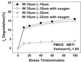
The impact of oxygen PDA on reliability was performed with PBI and NBI tests. In the PBI and NBI measurements, samples were stressed in gate terminal at 25 °C and VD= VS= VB= 0 V. And the
gate terminal voltages were VT+ 2.3 V and VT 1.8 V for PBI and
NBI, respectively. Figs.4 and 5 show the ID degradations under
PBI and NBI test, respectively. The oxygen PDA nMOSFET or pMOS-FET has a lower ID degradation than the control device for both
long channel device (gate length = 10
l
m) and short channel de-vice (gate length = 32 nm). This means the oxygen PDA could im-prove the worsen reliability issue under stress. Moreover, we found the oxygen PDA also suppressed the VTHshift under NBIand PBI tests. Therefore, we conclude that the reliability degrada-tions are strongly related to the traps in the HfO2 gate, but can
be repaired by the oxygen PDA.
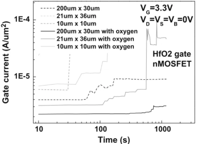
On the other hand, we investigated the effect of the oxygen PDA on trap generation during the reliability test with TDDB and field breakdown under a ramp voltage stress (RVS). A typical TDDB characteristic of an HfO2 gated NMOSFET stressed in VG= 3.3 V,
VS= VD= VB= 0 V is illustrated inFig. 6. Following the stress time
increase, we could define the characteristic into three regions i.e., fresh region, soft breakdown SBD region and hard breakdown (HBD) region, respectively. SBD and HBD have been found to be -1.5 -1.0 -0.5 0.0 0.5 1.0 1.5 1E-8 1E-7 1E-6 1E-5 1E-4 1E-3 0.01 0.1 1 10
V
D=0.05 V
W:10um L:10um HfO 2I
D(u
A
/u
m
)
V
G(volts)
nMOSWith Oxygen nMOS pMOS
With Oxygen pMOS
Fig. 1. ID/VGcurves of Hf-oxide gated nMOSFET and pMOSFET.
0.4 0.8 1.2 1.6 0 100 200 300 HfO2 gate 10um x 10um
M
o
b
ilit
y
(c
m
2/V
-s
)
Eeff (MV/cm)
NMOSNMOS with oxygen PMOS
PMOS with oxygen Universal
Fig. 2. Measured mobility vs. effective electric field for Hf-oxide gated nMOSFET and pMOSFET with and without the post oxygen treatment.
-1.5 -1.0 -0.5 0.0 0.5 1.0 1.5 0 30 60 90 120 150 0 30 60 90 120 150 W=200um L=30um
pMOS
EOT=17.4A
nMOS
EOT=16.8A
TiN/HfO 2Capacitance (pF)
V
G(V)
(nMOS) (nMOS) (pMOS) Without (pMOS) O 2 treatment annealFig. 3. Cox/VGcurves for Hf-oxide gated nMOSFET and pMOSFET with and without
the post oxygen deposition annealing. Similar EOT extracted from C–V curves was found for both with and without annealing devices.
0 20 40 60 80 100 0 5 10 15 20 25 30 35
NMOS PBTI
Vstress=V
T+2.3V
I
DDegradation(%)
Stress Time(minutes)
W:10um L:10um
W:10um L:10um with oxygen
W:10um L:32nm
W:10um L:32nm with oxygen
Fig. 4. For PBTI stress, less ID degradation was found on the Hf-oxide gated
nMOSFET with oxygen treatment.
0 5 10 15 20 25
PMOS NBTI
Vstress=V
T-1.8V
I
DDegradation(%)
Stress Time(minutes)
W:10um L:10um
W:10um L:10um with oxygen
W:10um L:32nm
W:10um L:32nm with oxygen
0 20 40 60 80 100
Fig. 5. For NBTI stress, less IDdegradation was found on Hf-oxide gated pMOSFET
with oxygen treatment.
dependent on the quality of interfacial layer and high-k layer, respectively[11]. SBD starts with the formation of a localized con-duction path in the interfacial SiO2layer and has multi unstable
conducting path. In SBD region, the gate stack does not whole breakdown, however, follows the voltage stress continuously, the traps localized areas increases and drives into high-k layer. In final, results in a gate punch through in the HBD region.
We combined a charge pumping system and TDDB test to in-spect the generation of defect traps. In the past, the charge pump-ing system was widely used to investigate interface defects[12]. As shown in the insert ofFig. 6, the curve of Icp shifts to positive and rises up in the SBD region. This means the trap defects were contin-ually generated from the fresh time to SBD time. However, as the stress time come to HBD region, the Icp could not be measured anymore for the huge defect traps and gate current. Thus, as indi-cated inFig. 7, the oxygen PDA could extend the time for TDDB obviously in different kinds of dimensions means the oxygen PDA could passivate a lot of interface states. Similar phenomena were also found under ramp voltage stress condition as shown in
Figs. 8 and 9for the field breakdown and the Icp current of charge pumping test, respectively. Again, both the breakdown characteris-tic and Icp current of the oxygen PDA device are better than the control device. Furthermore, the lower Icp for the oxygen PDA de-vice implies it has lower interface defects during the entire stress condition and thus can slow down the reliability degradation, including TDDB, NBI and PBI.
4. Conclusions
A post oxygen deposition annealing was proposed to enhance the Hf-oxide/metal-gate MOSFET device life time by passive oxide-related trap defects. The mechanism was evidenced by mea-suring the TDDB or field breakdown and Icp current in the same time. Thus, the device reliability issue can be improved by the oxy-gen deposition annealing. In addition, the oxyoxy-gen deposition annealing does not lower drive current or increase oxide thickness (EOT).
Acknowledgments
This work was supported by the National Science Council under Contract NSC98-2221-E-390-039, NSC96-2221-E-006-284-MY3 and NSC97-2221-E-006-244.
The authors would like to thank UMC staffs for their helpful supporting.
References
[1] Wilk GD, Wallace RM, Anthony JM. High-k gate dielectrics: current status and materials properties considerations. J Appl Phys 2001;89(10):5243–75. [2] Lee BH, Young CD, Choi R, Sim JH, Bersuker G, Kang CY, et al. Intrinsic
characteristics of high-k devices and implications of fast transient charging effects (FTCE), electron devices meeting, 2004. In: IEDM technical digest. IEEE international; 13–15 December 2004. p. 859–62. 0.000 0.005 0.010 0.015 -1.2 -0.8 -0.4 0.0 0.4 0.0 2.0x10⁻⁶ 4.0x10⁻⁶ 6.0x10⁻⁶ Fresh SBD HBD ICP (A ) VG (volts)
HBD
SBD
Fresh
HfO2 gate
nMOSFET
200um x 30um
Gate stress=3.3V
I
G(A
)
Time (Second)
0 200 400 600 800Fig. 6. TDDB test for the Hf-oxide gated nMOSFET. The insert shows the measured charge pumping current during the TDDB test.
10 100 1000 1E-5 1E-4
V
G=3.3V
V
D=V
S=V
B=0V
HfO2 gate
nMOSFET
Gate current (A/um
2
)
Time (s)
200um x 30um 21um x 36um 10um x 10um
200um x 30um with oxygen 21um x 36um with oxygen 10um x 10um with oxygen
Fig. 7. Less TDDB was found on the Hf-oxide gated nMOSFET with the post oxygen deposition annealing for various gate dimensions.
2 3 4 5 6 0.01 0.1
I
G(A
)
V
G(volts)
HfO
2gate
nMOSFET
200um x 30um
nMOS with Oxygen
nMOS
Fig. 8. IG/VGcharacteristics of the Hf-oxide gated nMOSFET under ramp voltage
stress. -1.0 -0.5 0.0 0.5 0.0 5.0x10⁻⁶ 1.0x10⁻⁵ HfO gate 200um x 30um Freq=1Mhz Amplitude=1V
Icp shift to positive, when increase stress bias
nMOS Bearkdown at 4.5V
nMOS with Oxygen Bearkdown at 5.3V
V
G(volts)
I
CP(A
)
Fig. 9. Less charge pumping current was found on the Hf-oxide gated nMOSFET with the post oxygen deposition annealing.
[3] Robertson J. High dielectric constant gate oxides for metal oxide Si transistors. Rep Prog Phys 2006;69(2):327–96.
[4] Kerber A, Cartier E, Pantisano L, Rosmeulen M, Degraeve R, et al. Characterization of the VT instability in SiO2/HfO2 gate dielectrics. In:
Proceeding 41st annual IEEE international reliability physics symposium; 2003. p. 41–5.
[5] Zafar S, Kumar A, Gusev E, Cartier E. Threshold voltage instabilities in high k gate dielectric stacks. IEEE Trans Dev Mater Reliab 2005;5(1):45–64. [6] Hokyung Park, Rino Choi, Seung Chul Song, Man Chang, Young CD, Bersuker G,
et al. Decoupling of cold carrier effects in hot carrier reliability of HfO2gated
nMOSFETs. In: Reliability physics symposium proceedings, 2006. 44th annual, IEEE international; 26–30 March 2006. p. 200–3.
[7] Sato M, Umezawa N, Shimokawa J, Arimura H, Sugino S, Tachibana A, et al. Physical model of the PBTI and TDDB of la incorporated HfSiON gate dielectrics with pre-existing and stress-induced defects. Electron devices meeting, 2008. IEDM 2008. IEEE international; 15–17 December 2008. p. 1–4.
[8] Torii K, Kitajima H, Arikado T, Shiraishi K, Miyazaki S, Yamabe K, et al. Physical model of BTI, TDDB and SILC in HfO2-based high-k gate dielectrics. Electron
devices meeting, 2004. In: IEDM technical digest. IEEE international; 13–15 December 2004. p. 129–32.
[9] Foster AS, Lopez Gejo F, Shluger AL, Nieminen RM. Vacancy and interstitial defects in hafnia. Phys Rev B 2002;65:174117.
[10] Xiong K, Du Y, Tse K, Robertson J. Defect states in the high-dielectric-constant gate oxide HfSiO4. J Appl Phys 2007;101(2) [Article No. 24,101].
[11] Bersuker G, Chowdhury N, Young C, Heh D, Misra D, Choi R. Progressive breakdown characteristics of high-k/metal gate stacks. IRPS 2007:49–54. [12] Xiong HD, Heh D, Gurfinkel M, Li Q, Shapira Y, Richter C, et al. Characterization
of electrically active defects in high-k gate dielectrics by using low frequency noise and charge pumping measurements. Microelectr Eng 2007;84:2230–4. C.-W. Hsu et al. / Microelectronics Reliability 50 (2010) 618–621 621