在20 GHz以上射頻IC應用上與CMOS製程相容的介電支撐物質製程開發與研究
32
0
0
全文
(2) 在 20 GHz 以上射頻 IC 應用上與 CMOS 製程相容的介電支撐物質 製程開發與研究 A CMOS Compatible Patterned Dielectric Beyond. 20GHz. Silicon. Support Process for. RFIC. Applications. 研 究 生:陳思穎. Student:Ssu Ying Chen. 指導教授:鄭裕庭. Advisor:Yu-Ting Cheng. 國 立 交 通 大 學 電子工程學系電子研究所 碩 士 論 文. A Thesis Submitted to Department of Electronics Engineering & Institute of Electronics College of Electrical and Computer Engineering National Chiao Tung University in Partial Fulfillment of the Requirements for the Degree of Master In Electronics Engineering October 2006 Hsinchu, Taiwan, Republic of China. 中華民國九十五年十月.
(3) 在 20 GHz 以上射頻 IC 應用上與 CMOS 製程相容的介 電支撐物質製程開發與研究 學生:陳思穎. 指導教授:鄭裕庭教授. 國立交通大學電子工程學系暨電子研究所碩士班. 摘. 要. 在現今的通訊晶片發展過程裡,SOP 技術已經有相當程度的發展;然而 當我們把被動微波元件實現在低阻值的矽晶圓上時,矽基底所造成的能量 損失已經讓此被動元件無法得到可應用的效果,也因此,各方都在找一個 既便宜又有效果的解決辦法來改進此種現象帶來的缺失;而在徹底了解形 成此基底效應的機制以及發展至今各方學界所發表的解決辦法之後,到目 前為止,並沒有一個真正有個可以兼顧機械以及電性的方法來改善;因此, 我們發展了一套利用一般常見的介電物質(二氧化矽、氮化矽)以及柵狀結 構來有效的減少基底效應,而建築在此構造上的微波元件也都能達到我們 想要的結果。此外,在本篇論文裡,我們更利用了介電物質的特性來達到 可以減少一道製程,這也大大的減少此種製程的便利性;而表現出來的高 頻特性(1~40. GHz)更可以與一般印電路板相同的達到幾乎沒有. 能量的損失;在製程方面,利用了微機電製程中的感應耦合電漿蝕刻機(I CP. DRIE) 、高溫爐管以及低壓化學沉積系統LPCVD來得到支撐. 1.
(4) 的介電柱狀結構,由以上可知,製程上更有與CMOS製程有相容性的優 點,因此利用這個製程可以在 SOP 的應用上達到理想的效果。. 2.
(5) A CMOS Compatible Patterned Dielectric Support Process for Beyond 20GHz Silicon RFIC Applications Student : Ssu Ying Chen. Advisor : Yu-Ting Cheng. Department of Electronics Engineering & Institute of Electronics National Chiao Tung University. Abstract A powerful reducing substrate loss method, trenched oxide-nitride islands, was demonstrated using CMOS-compatible fabrication process. The CPW on trenched oxide-nitride islands can achieve insertion loss as low as 0.045dB/150um at 40 GHz on low resistivity silicon substrate if we can solve the roughness problem. The simulated result of inductor comparison between on our design structure and conventional Si predict the improvement of inductor performance. Another advantage of trenched oxide-nitride islands is that can possess strong mechanical support and better reliability than the suspended structure Index terms —RF MEMS, eddy current, coplanar waveguides, Bosch process, trenched dielectric islands. 3.
(6) 誌. 謝. 首先,我想要感謝在交大電子所認識的每一個人;我的指導教授鄭裕庭 老師,不管是您的思考路線或者是您帶學生方式,都帶給我無限的啟發以 及成長;教授我AIC的吳介崇教授,您讓我更深入的了解到電子電路神 奇之處;實驗室的趙子元學長,這兩年來幾乎都靠你來解決我們研究上的 問題;RFIC實驗室的傅昶綜學長,您在MTK報告中對問題的看法讓 我大開眼界;實驗室的阿拉拉建章學長,你對理論的熱忱就跟你的阿拉拉 一樣滔滔不絕,讓我甘拜下風;畢業的光哥、瑋哥、川哥,沒有你們的努 力我們沒有那麼多資源可以使用;躲桌子的達叔,福爾摩沙代言人的凱哥, 謝謝您們在畢業後還如此關心我的研究;實驗室的榮譽博士生小筑,謝謝 妳在必須周旋在眾男人的閒暇之餘,能夠聽我大吐苦水;同屆的特助 chando,即使你在我最低潮的時候依然不改嘴賤的本事,但卻也讓我成長了 許多;球速破百的火球男小B,你讓我漸漸懂得要如何觀賞設計的品味; 龜縮的昱文,你那變化莫測的睡覺姿勢以及高腰褲可說是讓我大開眼界 了;以及實驗室各個學弟妹們,你們對我的鼓勵我都很感激,實驗室接下 來就靠你們了;陶藝社的宗凰、健誠等各位朋友,謝謝你們讓我在枯燥的 研究生活中還能殘留一點大學生涯的元素;以及大學山服社的好朋友們, 跟你們在一起的時光讓我可以隨時的補充能量,尤其是在這我人生最低潮 的一年半中,能夠忍受我近乎白痴又無法控制的個人行為並且陪著我一步 步走出低潮;每一位在交大所認識的人,都讓我點滴在心頭,謝謝你們充 實了我這兩年的生活。 最後,要感謝我的母親,忍受著兒子一年回家兩次的不孝行為,沒有您, 就沒有今天的我;而最低潮的時間已經過去了,明天的我,會努力讓您感 到驕傲的。. 4.
(7) Contents 摘要. 1. Abstract. 3. 誌謝. 4. Contents. 5. Figure Captions. 6. Table Captions. 7. Contents Chapter 1 Introduction. 8. Chapter 2 Concept Design. 13. Chapter 3 Fabrication. 16. Chapter 4 Discussions. 19. Chapter 5 Measurement and simulation. 23. Chapter 6 Conclusion and Future Work. 26. References. 27. 5.
(8) Figure Captions Chapter 2 Figure.1 Figure1.simulated current distribution………………………………7 Figure 2 (a) layout of trenched oxide-nitride islands (b) the SEM picture……8. Chapter 3 Figure 3. (a)Deep trench etching by Bosch process. (b)thermal oxide grown. (c)ICP etching resident silicon. (d) LPCVD deposit nitride. (e)electroplate CPW…………………………………………………..10 Figure.4 The SEM picture of oxide-nitride islands………………………….....11 Figure.5 copper electroplated on islands directly…………………………..…..11. Chapter 4 Figure.6 SEM picture of rooting phenomenon without controlling………..…..14 Figure 7. The lithography diagram of trenched island deposited seed layer…...14 Figure 8. the SEM picture of rooting phenomenon with controlling exposed time…………………………………………………………………....15. Chapter 5 Figure 9. the measurement and simulation result of 150um CPW on the trenched oxide-nitride islands…………………………………………………..17 Figure 10. The S21comparison between the CPWs on different substrates...….17 Figure11. The simulated comparison of the inductors between that on conventional Si substrate and on trenched oxide nitride islands……...18. Chapter 6 Figure 12. the filter on the oxide-nitride islands……………………………….27 6.
(9) Table Captions Chapter 1 Table 1 Comparison of several methods for reducing substrate loss………...….5. Chapter 4 Table 2 The contact angle of DI water on islands………………………..…….12. 7.
(10) Chapter 1 Introduction Inevitable substrate loss mechanism is one of major factors hinder silicon based RFIC technology for high frequency wireless communication applications. Poor passive components on Si-RFIC due to the substrate loss like low Q inductor, filter, and high loss TML (Transmission Line) could result in a circuit performance with smaller dynamic range, higher noise figure, and larger power consumption which would make the circuit hard to be applied for high speed data communication.. Besides, the loss phenomenon will become more severe. with the increase of operational frequency of the circuit.. Therefore, a lot of. research efforts have been put for eliminating the substrate loss mechanism. For examples, proton implanted silicon substrate can have higher resistivity than conventional Si substrate which makes the on-chip passives perform well and consistently up to 40 GHz [1], The silicon substrate with patterned ground shields can effectively enhance the Q performance of on-chip spiral inductor up to 10 GHz [2], and the others like silicon trenched islands, nitride blocks [4], pn junctions isolation [5], and suspended membrane support… etc., can all provide nice approaches for high performance passive fabrication.. Nevertheless, while. the frequency rises up to 40 GHz or even higher, only the membrane support with substrate removal and proton implanting methods are effective to eliminate the loss issue. Among the above approaches, removing the substrate under the microwave. 8.
(11) device directly is the most popular and well-developed technology using contemporary micromaching process.. Since the substrate under the device is. removed, as suspended structure or membrane structure, the resistivity of “substrate” (air) raises so high that it is very difficult to generate the eddy current due to the variation of magnetic flux. The less the eddy current, the less energy dissipated from substrate.. On the other hand, the parasitic capacitor. between the upper transmission line and substrate also decreases a lot. J. Y.-C. Chang etc. published the high Q large suspended inductor encased in oxide on a membrane over the substrate with the removal of underlying silicon in 1993[7], although it is for 2um CMOS RF amplifier. It has been proved that the quality factor and self-resonace can be improved when substrate removed. In 1998, Pieere Blondy published the high performance filter with removing the dielectric material up to a thin membrane that suspends the planar filters. [6]. he used the membrane made of ONO (oxide-nitride-oxide) structure, etching underlying silicon substrate, and two metalized cavities as upper and lower shielding. The combination of bulk micromaching by removal of the substrate and self packaging reduces the radiation loss both into air and substrate and also greatly reduces ohmic loss by allowing for very wide microstrip lines. The filters he designed consist of a 3.5%bandwidth two-pole Chebyshev filter with transmission zeros at 37 GHz, 2.7% and 4.3% bandwidth four- and five-pole Chebyshev filters at 60 GHz, and an 8% bandwidth elliptic filter at 60 GHz.. 9.
(12) To date, many applications of suspended structure are post, tabled in table 1, for example, Hongrui Jiang etc. published the inductor suspended over the deep copper-lined cavities over 30-um deep.[8] They built a suspended inductor over a cavity whose bottom plane and sidewalls are metallized with copper. The deep cavity reduces the electromagnetic coupling and parasitic capacitance between the inductor and substrate that can increase quality factor and self-resonace. And the Cu-lined provide electromagnetic shielding. The quality factor of the inductor is over 30 and self-resonace frequency is 10 GHz. Moreover Jun-Bo Yoon etc. published a highly suspended spiral inductor in 2002[9]. The inductor was lifted 50um in height without any membrane and only suspended by two signal posts of 20 um in diameter without any additional mechanically supporting posts in order to minimize the substrate coupling. And the quality factor of the highly lift inductor is up to 70 at 6 GHz and it’s self-resonace frequency is over 20 GHz. Although the above suspended structures are so sensitive to the vibration of environment, it is not suitable for the portable communication technology due to lack of electrical and mechanical reliabilities. So, in 2005, Mina Raieszadeh published the trenched silicon island structure [3], which the inductor is supported by trenched silicon islands and the Q of the inductor is about 51 at 1 GHz It solved the vibration issue of suspended device. But the microwave device on this structure will suffer from the increasing substrate loss when the. 10.
(13) frequency is higher frequency. It is because there is still silicon substrate contacted the device, that parasitic capacitor makes the operation frequency down. In this paper, we will use the oxide-nitride islands patterned substrate and electroplate the Cu CPW on the patterned substrate. With oxide-nitride islands patterned substrate, we not only reduce the substrate loss due to it’s isolation property but also electroplate the Cu CPW on the islands directly due to the small space of the gaps between neighbor islands. Better transmission line performance (1 GHz to 50 GHz) on oxide-nitride islands patterned substrate than those on silicon substrate are evidenced.. 11.
(14) Design. Author. Advantage. Weak-point. Pierre Blondy. High performance up to 60 GHz. Weak to vibration and process complicated cost. Photon implanted substrate. Albert Chin. High performance up to 40 GHz. Patterned ground shielding. High Q inductor at C. Patrick 1~10 GHz Yue. SiRN/SiRN -Si block. Very thick Operation dielectric layer frequency M Elwensp-o lower ek. Membrane with metallized shielding. Pn junction Min Hao isolation. Improve Qs of inductor 19%. Operation frequency lower. High Q inductor at 1~10 GHz. Operation frequency lower. Trenched silicon island. Farrokh Ayazi. Edgesuspended CPW. High Lydia L. performane W. Leung CPW at 1~ 40G. Table1- comparison of several methods for reducing substrate loss. 12. Operation frequency lower. Complicated applied for passive component.
(15) Chapter 2 Concept Design At microwave frequency, the variation speed of magnetic flux is so fast that induced eddy current in the silicon substrate with opposite direction to signal flow will convert magnetic energy into heat, so called substrate loss. Equation 1 and 2 show the element of induced current in substrate at the presence of electromagnetic fields [10]. ∇ × H = jωε' E + ωε' ' E tanδ + σE. [1]. ∇ × E = − j ωμ H , J = σ E. [2]. Where σ and tanδ represent the substrate conductivity and loss tangent,ε’andε”are the real and imaginary part of the substrate permittivity, ω is the angular frequency, and μ is the permeability. For CMOS-grade silicon, the σE term which represent the electrically-induced current dominates over the terms ωε’Etanδ which represent the dipole loss. Thus, we will effective reduce the substrate effective permittivity and conductivity by oxide-nitride island. Because slicing the substrate with deep high-aspect-ratio trenches, the path of induced current is disrupted that reduces the substrate effective permittivity and conductive which in turn reduces the electrically and magnetically-induced current as well as the dipoles. For higher frequency application, we further make the dielectric island to reduce the substrate loss. At DC and low frequency, the current is uniformly distributed. When. 13.
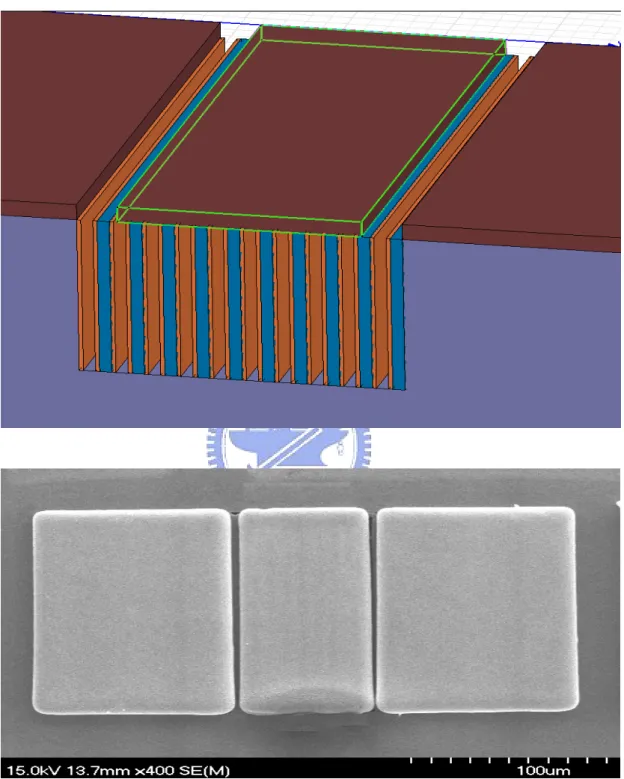
(16) frequency raises higher and higher, skin effect becomes significant, so that AC current is pushed towards the edges of signal line. Figure 1. shows the current distribution simulation of conventional CPW at 10 GHz with HFSS. Most of current is concentrated along the two edge of signal line. But if for other microwave device, for example inductor or filter, we could not replace dielectric material only for the substrate under the edge of signal line. Figure 2 shows the layout of trenched oxide-nitride islands design .With this structure, we can exactly reduce the substrate loss for any microwave device on the silicon.. Figure1.simulated current distribution. 14.
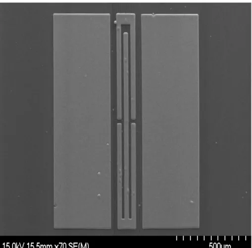
(17) Figure 2 - (a) layout of trenched oxide-nitride islands (b) the SEM picture. 15.
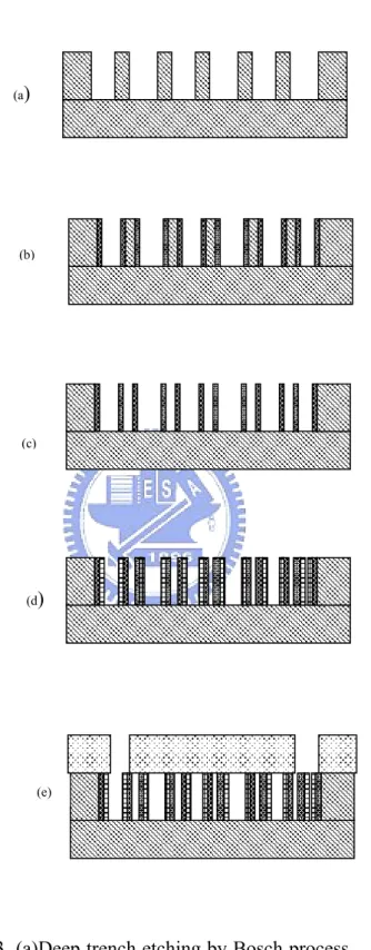
(18) Chapter 3 Fabrication Figure3 shows the fabrication process flow for the CPW on the trenched oxide-nitride islands. First, deep high-aspect-ratio (10:1) trenches are etched by ICP DRIE,so called Bosch process. Then 1.3um thick thermal oxide is grown at 1100°C and using RIE to etch the upper horizontal oxide layer. At present, we can get the trenched silicon-oxide islands. After patterned the etching hole, we use ICP-DRIE to etch the resident silicon of silicon-oxide islands. Then deposit the silicon nitride by using LPCVD (Low pressure chemical vapor deposition). Because of the high covering property of LPCVD, we can get the oxide coated with nitride, oxide-nitride islands shown as figure 4. After using e-gun to deposit seed layer, we can electroplate CPW directly because nitride is hydrophobic shown as figure 5.. 16.
(19) (a). (b). (c). (d). (e). Figure 3. (a)Deep trench etching by Bosch process. (b)thermal oxide grown. (c)ICP etching resident silicon. (d) LPCVD deposit nitride. (e)electroplate CPW. 17.
(20) Figure.4 The SEM picture of oxide-nitride islands. Figure.5 copper electroplated on islands directly. 18.
(21) Chapter 4 Discussions 1. Electroplate copper without membrane Because of the hydrophobic property of silicon nitride, we consider that by this property with designation we will make the electroplating solution separated from the trench due to the surface tension force. In order to confirm that the tension force of water on nitride is enough to make water not flowing into trench, we measure the contact angles of DI water on the patterned silicon-nitride islands as shown table-2. Contact angle Silicon island. Nitride island. Height (mm). Sessile volume (uL). 5-5 84.9. 1.1899. 4.9927. 5-4 84.5. 1.2045. 5.3562. 5-3 88.07. 1.219. 4.432. 5-2 91.65. 1.277. 5.014. 4-3 91.04. 1.3205. 5.2238. 5-5. 79.97. 1.1319. 5.1368. 5-4 81.49. 1.1899. 5.5119. 5-3 80.80. 1.1319. 4.947. 5-2 81.10. 1.1754. 5.1165. 4-3 80.13. 1.2045. 5.6933. Table-2 the contact angle of DI water on islands. 19.
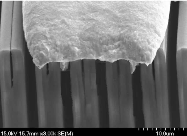
(22) 2. rooting phenomenon Although nitride is hydrophobic, the seed layer e-gun deposited before electroplating is hydrophilic. Thus, there is some copper electroplated on the sidewall of the trenched oxide-nitride islands. On the other hand, the copper is electroplated into the trenches, that makes the CPW like rooting. Figure 6.shows this rooting phenomenon clearly. Undoubtedly, this rooting part will influence the performance of main upon CPW. There are some un-anticipated parasitic effects between the rooting copper areas, and the uncontrolled characteristic impedance will make microwave devices designation difficult. Thus, we will solve this problem by controlling the lithography time. As figure 7 shows, the top of islands deposited seed layer does reflecting more UV, that makes the photoresist(AZ 4620) upon. the islands effectively exposed twice as the. photoresist upon the tenches only exposed once. So, we can control the exposed time to make the photoresist upon the islands hyper-exposed and that upon the trenches hypo-exposed, and can prevent the sidewall electroplated with copper. Figure 8 shows the improvement of rooting phenomenon. Obviously the rooting areas decrease, and the surface of CPW upon the structure is more smooth that make the performance of CPW better.. 20.
(23) Figure.6 SEM picture of rooting phenomenon without controlling. Si Seed layer. Figure 7. The lithography diagram of trenched island deposited seed layer. 21.
(24) Figure 8. the SEM picture of rooting phenomenon with controlling exposed time. 22.
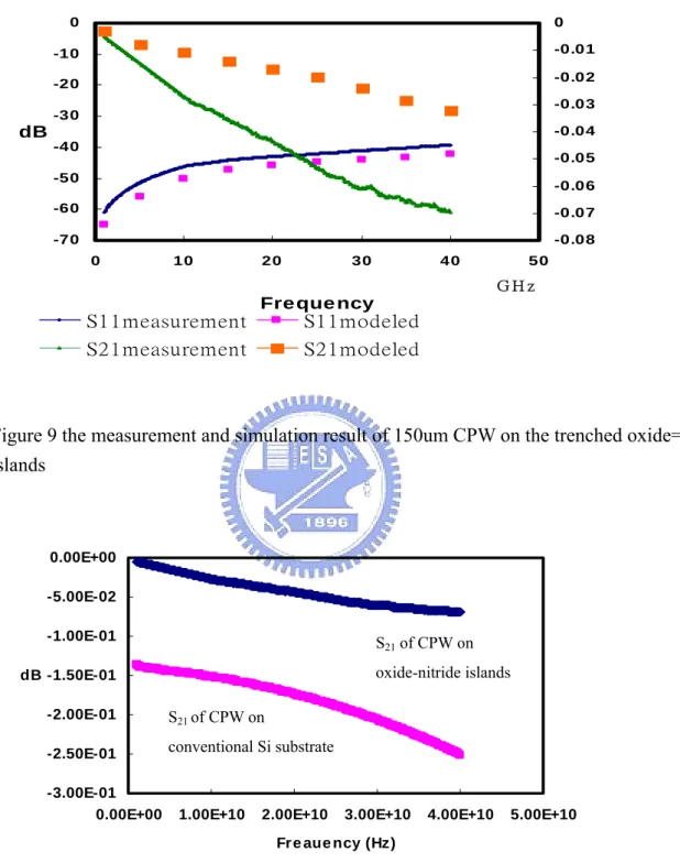
(25) Chapter 5 Measurement and Simulation Simulated and measurement results of 150um CPW are shown as figure9. As we predicted previously, at 40 GHz the insertion loss of CPW is so small (S21~0dB) and the return loss is also very tiny from 1 GHz to 40 GHz. Noted that, the measurement result differs from simulation result, S11 is higher and S21 is lower slightly. It’s because the degree of roughness of CPW is not uniform and there are some inversion rooting areas under the CPW. The comparison of the loss of CPW on oxide-nitride islands and that on conventional Si substrate is shown as figure 10. We can see the huge improvement of S21, that is due to the substrate loss reduced effectively.. 23.
(26) 0. 0. -10. -0.01. -20. -0.02 -0.03. -30. dB. -0.04 -40. -0.05. -50. -0.06. -60. -0.07. -70. -0.08 0. 10. 20. 30. 40. 50. GHz. S11measurement. Fre que ncy. S11modeled. S21measurement. S21modeled. Figure 9 the measurement and simulation result of 150um CPW on the trenched oxide=nitride islands. 0.00E+00 -5.00E-02 -1.00E-01. S21 of CPW on oxide-nitride islands. dB -1.50E-01 -2.00E-01. S21 of CPW on. -2.50E-01. conventional Si substrate. -3.00E-01 0.00E+00. 1.00E+10. 2.00E+10. 3.00E+10. 4.00E+10. 5.00E+10. Fre aue ncy (Hz). Figure 10 The S21comparison between the CPWs on different substrates. 24.
(27) In additional, we simulate a microwave device, inductor, on the trenched oxide- nitride islands to predict the effect of the inductor on trenched oxide-nitride islands. As figure11 shows, when the substrate replaced by trenched oxide-nitride islands the quality factor and self-resonance frequency of the inductor are improved. This is obviously because the parasitic conductance between the copper and substrate reduces with the reducing contact areas.. 4.00E+01. 8.00E-08. 3.00E+01. 6.00E-08. 2.00E+01. 4.00E-08. 1.00E+01. 2.00E-08. Q 0.00E+00. 0.00E+00 (H). -1.00E+01. -2.00E-08. -2.00E+01. -4.00E-08. -3.00E+01. -6.00E-08. -4.00E+01 -8.00E-08 0.00E+00 5.00E+09 1.00E+10 1.50E+10 2.00E+10 2.50E+10 Fre que ncy(Hz) Figure11. the simulated comparison of the inductors between that on conventional Si substrate and on trenched oxide nitride islands. 25.
(28) Chapter 6 Conclusion and Future Work 6.1 Conclusion A powerful reducing substrate loss method, trenched oxide-nitride islands, was demonstrated using CMOS-compatible fabrication process. The CPW on trenched oxide-nitride islands can achieve insertion loss as low as 0.045dB/150um at 40 GHz on low resistivity silicon substrate if we can solve the roughness problem. With PECVD, we can deposit an oxide layer to solve the non-smooth problem. Thus the trenched oxide-nitride islands can provide even smaller. insertion. loss,0.045dB/150um.Another. advantage. of. trenched. oxide-nitride islands is that can possess strong mechanical support and better reliability than the suspended structure.. 6.2 Future Work Because the substrate under CPW is not simple as silicon , the filter design will be improve to make the performance of filter better and better as shown in figure 12. We can utilize the design of trench pattern to make the Z0 of upper CPW designed , so that can use stepped-impedance method to design filter. We can utilize this process to improve the Q of spiral inductor on Si .. 26.
(29) Figure 12. the filter on the oxide-nitride islands. 27.
(30) References 1. K. T. Chan, C. Y. Chen, Albert Chin, Senior Member, IEEE, J. C. Hsieh, J. Liu, T. S. Duh, and W. J. Lin, “40-GHz Coplanar Waveguide Bandpass Filters on Silicon. Substrate”, Microwave and Wireless Components. Letters, IEEE Volume 12,. Issue: 11 page(s): 429- 431 Nov 2002. 2. C. Patrick Yue, Student Member, IEEE, and S. Simon Wong, Senior Member, IEEE, “On-Chip Spiral Inductors with Patterned Ground Shields for Si-Based RF IC’s”, IEEE Journal of solid-state circuits,. 33(5):743-752, May 1998 3. Mina Raieszadeh, Pejman Monajemi, Sang- Woong Yoon, Joy Lash-ur, and Farrokh Ayuz, “HIGH-Q INTEGRATED INDUCTORS ON TRENCHED SILICON ISLANDS”, IEEE Int. Conf. on Microelectromechanical Systems. (Miami, USA, Jan. 2005) pp 199–202 4. L.J. Ferna’ndez, E. Berenschot, J. Sese’, R.J.Wiegerink,J. Flokstra, H.V. Jansen and M. Elwenspoek, “Fabrication of thick silicon nitride blocks for integration of RF devices”, Electronics Letters 41, 124 (2005) 5. Hongyan Jian*, Zhangwen Tang, Jie He, Jinglan He, Min Hao, “Standard CMOS Technology On-chip Inductors with pn Junctions Substrate Isolation”, 2005 IEEE Asia South Pacific Design Automation Conference Proceedings, pp. D-5 - D-6, Jan. 2005. 6. Blondy, P.; Brown, A.R.; Crost, D.; Rebeiz, G.M.;Large, . “Low loss micromachined filters for millimeter-wave Telecommunicationsystems”, IEEE Trans. Microwave Theory Tech., Vol. 46, pp. 2308-2316, Dec. 1998. 7. Chang, J.Y.-C.; Abidi, A.A.; Gaitan, M., “Suspended inductors on silicon and their use in a 2-μm CMOS RF amplifier”, IEEE Electron Device Lett.,1993;14:246-248. 8. Hongrui Jiang; Ye Wang; Yeh, J.-L.A.; Tien, N.C., “On-chip spiral inductors suspended over deep copper-lined cavities”, Microwave Theory and Techniques, IEEE Transactions onVolume 48, Page(s):2415 – 2423. 28. Issue 12,. Dec. 2000.
(31) 9. Jun-Bo. Yoon;. Yun-Seok. Choi;. Byeong-Il. Kim;. Yunseong. Eo,. “CMOS-compatible surface-micromachined suspended spiral inductors for multi-GHz. silicon. RF. ICs”,. IEEE. Electron. Lett,2002;23(10):591-593. 10. D.M. Pozar, “Microwave Engineering”, John Wliley&Sons,2005.. 29. Device.
(32) Vita 姓. 名:陳思穎 (Ssu Ying Chen). 出生日期:中華民國七十一年三月四日 出 生 地:台灣省台南市 E - mail:[email protected] 學. 歷: 國立台南第一高級中學. (1998.9~2000.6). (National Tainan first High School) 國立清華大學材料工程學系. (2000.9~2004.6). (National Tsing Hua University) 國立交通大學電子工程所碩士班. (2004.6~2006.10). (Department of electronics Engineering & Institute of Electronics, Nation Chiao Tung University). 30.
(33)
數據

+3
相關文件
運用 Zuvio IRS 與台日比較文化觀點於日本文化相關課程之教學研究 Applying Zuvio IRS and Perspective on Cultural comparison between Taiwan and Japan to Teaching
The bottleneck stations with multiple machines are generally in the industry, such as semiconductor wafer manufacturing plants, IC substrate manufacturing plants,
GaN transistors with high-power, High temperature, high breakdown voltage and high current density on different substrate can further develop high efficiency,
研究與發展(research and development, R&D) 係指進步的 科學知識或產品(與製程)之創新而言[23]。依據美國國家科學基 金會的報告,顯示在最近
第二章是介紹 MEMS 加工製程,包括體型微加工、面型微加工、LIGA、微 放電加工(Micro-EDM)、積體電路相容製造技術 CMOS MEMS 製程等。製作微 加速度感測器。本研究是選用台積電 0.35μm
Atomic structure of hydrous ruthenium oxide coating on CNT substrate with 5 minutes of deposition period, (a) HRTEM image of specimen and (b) higher magnification of HRTEM
和 GSP 及 Graphmatica 類似,但過去有關電腦輔助教學的研究大多使用 GSP 設 計課程,在比較兩者的優劣之後,發現 GeoGebra 在使用上較 GSP
為完成上述研究目的,本文將於第二章依序說明 IPTV 的介紹與現況,以及詳述 e-SERVAUAL
