IEEE Asian Solid-State Circuits Conference November 16-18, 2009 / Taipei, Taiwan
978-1-4244-4434-2/09/$25.00 ©2009 IEEE 173
6-4
An 8 Gbps Fast-Locked Automatic Gain Control
for PAM Receiver
Guo-Wei Wu, Wei-Zen Chen, and Shih-Hao Huang
Department of Electronics Engineering, National Chiao Tung University, Hsin-Chu, 300, Taiwan
Abstract — An 8 Gbps automatic gain control (AGC) loop for
PAM receiver is proposed. Incorporating digital intensive gain control scheme, the dynamic range of the variable gain amplifier is 22 dB with a resolution of 0.9 dB/step. The locking time of the AGC loop is less than 200 ns and independent of input amplitude. Fabricated in a 0.18 μm CMOS technology, the chip size is 0.62
mm x 0.62 mm. The total power dissipation is 84 mW from a 1.8 V supply.
Keywords — automatic gain control (AGC), variable gain amplifier, PAM receiver.
I. INTRODUCTION
Multi-channel optical links suffer from less cross talk and EMI compared to their electrical counterparts, and are considered as promising technologies for data intensive platform and ultra high speed chip to chip interconnects. To take these advantages, low cost and small form factor optical transceivers incorporating silicon photo detectors are key components to enable pervasive adaptation. However, the intrinsic bandwidth of CMOS detectors in general is limited below hundreds of MHz. For over Gbps operations, they usually demand sophisticated equalization scheme [1]. In order to circumvent the speed limitation of the detector, optical link incorporating pulse amplitude modulation (PAM) can improve its spectral efficiency so as to boost up the data bandwidth. In this scenario, an AGC loop is needed to replace conventional limiting amplifier in the receiver chain. On the other hand, the locking speed of the gain control loop is also of special interests to retain its channel efficiency [2].
This paper presents the design of an automatic gain control loop for PAM receiver. Digital intensive gain control scheme and digital loop filter are adopted to accelerate locking speed while reducing chip area. It achieves less than 200 ns locking time independent of input amplitude variation.
This paper is organized as follows. Section II describes the AGC architecture. Section III describes the circuit schematic. The experimental results are shown in Section IV. Finally, conclusion is drawn in Section V.
II. AUTOMATIC GAIN CONTROL ARCHITECTURE
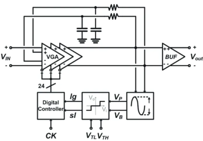
Fig. 1 illustrates the automatic gain control loop architecture (AGC), which is composed of a 3 stages variable gain amplifiers (VGA), an amplitude detector, a level comparator, an offset cancellation circuit, and a digital controller. The amplitude detector output is compared to reference voltages VTH and VTL, so as to digitally tune the VGA
gain by sending the control signal (lg, sl).
Typically, the VGA gain control scheme in terms of control voltage or control code should be linear in dB for a constant settling time [3]. In general, the settling time is compromised with the amplitude accuracy for a constant loop bandwidth. In order to circumvent this trade off, the proposed AGC loop undergoes binary gain searching mode and linear gain tracking mode during the amplitude locking process, which is moderated by the digital controller. Besides, to speed up the amplitude detection process, dual band peak and bottom hold detector are adopted for the amplitude detection [4].
This work is supported in part by National Science Council, Ministry of Economic, Mediatek, and TSMC.
174
III. CIRCUIT SCHEMATIC
A. Variable Gain Amplifier
Fig. 2 (a) shows the architecture of the variable gain amplifier, which is composed of a variable transconductance input stage followed by a transimpedance gain stage. The VGA gain Av can be approximated as
mf mi
v G
G
A = (1)
Fig. 2 (b) shows the variable transconductance stage by source coupled pair with digitally tunable resistor Rsi. For Av to be linearly tuned in dB scale, it turns out that the transconductance should be adjusted in a similar fashion as well. In this design, the Rsi is composed of a bank of triode region MOSFETs in parallel, which are scaled with a constant geometric ratio. As the turn on resistance (Rsi) of the degeneration MOSFET is inversely proportional to its aspect ratio, while its parasitic capacitance (Csi) is proportional to the device size. It concludes a relative constant zero frequency in the input transconductance stage. Another benefit is that the feedback factor of the transimpedance gain stage is kept constant, it minimizes gain peaking under different gain mode. Moreover, compared to VGAs employing Gilbert cell current
divider [5], the proposed configuration can prevent the input transconductance stage from being overloaded.
The tranimpedance gain stage is composed of voltage amplifier with active shunt feedback. For a maximum flat gain response, the -3 dB bandwidth of the voltage amplifier should be at least times higher than the overall VGA bandwidth. In order to achieve wide bandwidth performance, the voltage amplifier is configured as another active feedback Cherry-Hooper amplifier, resulting in a nested feedback architecture. It provides another flexibility to equalize phase response and minimize group delay variations.
B. Amplitude Detector
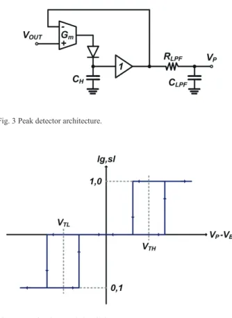
To speed up the acquisition of the signal amplitude, the amplitude detector is composed of peak detector, bottom detector, and a dual band low pass filter [4]. Fig. 3 shows the architecture of the peak detector. The Gm stage along with the
diode is configured as a negative feedback rectifier. In the initial state and during gain mode switching, the holding capacitor (CH) for peak detector is preset to a low level, while
that for the bottom detector is precharged to a high level. To avoid charge sharing effect, the signal amplitude is derived by a unity gain buffer followed by a dual band low pass filter (RLPF and CLPF). Here RLPFis also automatically adjusted by
digital controller during the amplitude locking process, leading the loop bandwidth to be changed from a wide band mode to a narrow band mode during gain tracking.
Fig. 2(a) Variable gain amplifier.
Fig. 2(b) Variable transconductance cell.
Fig. 3 Peak detector architecture.
Fig. 4 Transfer characteristic of tri-state comparator. Fig. 3 Peak detector architecture.
175 C. Comparator
The detected VGA output amplitude is compared to reference voltage level for gain adjustment. As the VGA is digitally tuned, to avoid gain mode flipping during the tracking process caused by the finite resolution of amplitude detector and gain mode quantization error, a tri-state comparator is adopted in this design. It provides holding mode when the output amplitude is approaching the target level.
Fig. 4 shows the transfer characteristic of the tri-state comparator. It is comprised of two hysteresis comparators with two threshold levels, VTH and VTL, which are determined by the
resolution of the gain mode. As the output amplitude is larger than VTH, lg (large) flag is raised and the VGA gain will be
reduced. Contrarily, if the detected amplitude is smaller than VTL, sl (small) flag is raised to increase the overall gain. If the
detected signal level falls between VTH and VTL, the AGC loop
will be kept in the hold mode. D. Digital Controller
To further accelerate the locking process, the AGC loop undergoes binary gain tuning and linear gain tracking during the locking process, which is moderated by the digital controller. The digital controller mainly comprises timing control unit and digital loop filter. The timing control unit generates control signal for the amplitude detector to preset peak/bottom detector. It also generates internal clock for the
searching engine and finite state machine to change gain tracking mode.
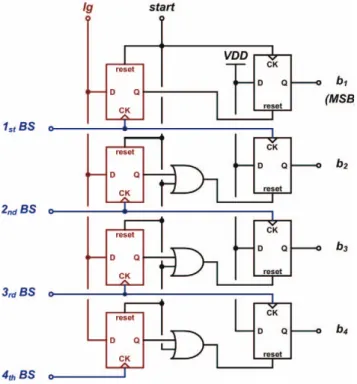
As the gain resolution of the VGA is targeted for about 1 dB/step, the total conversion gain is adjustable in 24 steps. Concerning the hardware complexity and settling time of the AGC loop, a 4-time binary search is chosen in this design. The most appropriate 16 bits thermometer code will be determined after binary search, and the remaining 8 control bits is controlled by the linear search engine to provide long term stability. Fig. 5 illustrates the 4 bits binary search engine, enabled by the start signal during the binary search mode. Here the searching algorithm can be simplified as the following steps:
(1) Preset the digital output (b1, b2, b3, b4) as (1,0,0,0). (2) For the ith binary search step (rising edge of ith BS), bi+1 is
preset to 1. Meanwhile, bi is kept one or reset to zero
depends on lg.
The linear search engine in this design is based on shift register, which resembles digital low pass filter in the AGC loop. The shift register will be shifted left or right depending on the control signal (lg, sl). It enables the increase or decrease of the conversion gain when the filter is overflow or underflow, and then resumes the register to its initial value for continuously gain mode tracking
Fig. 5 Binary search engine.
Fig. 6 Measured magnitude response of 16 different gain mode.
176
IV. EXPERIMENTAL RESULTS
The frequency response of VGA is characterized using Agilent E8364B network analyzer. Fig. 6 shows the measured frequency response under different gain modes. The -3 dB bandwidth of the VGA is about 4 GHz and is relatively constant across different gain modes, which is sufficient for 8-Gbps 4-PAM data rate.
To comply with the application of PAM optical link, the AGC provides a variable gain ranging from 1.9 dB to 24.2 dB. It corresponds to an input dynamic range of about 22 dB. Under 24 step gain control, the resolution for VGA is 0.9 dB/bit.
For the characterization of AGC, 4-PAM input data is generated by Tektronix arbitrary waveform generator (AWG) 7102. Fig. 7 shows the measured 8-Gbps 4-PAM eye diagram at the input sensitivity level. In this worst case, the VGA delivers the highest gain of about 24.2 dB and provides constant differential output swing of about 500 mVpp. The eye
height is about 130 mV.
The measured settling behavior of the AGC loop is shown in Fig. 8. The AGC loop undergoes binary searching mode followed by linear tracking mode for amplitude recovery. Under different input signal level, the measured settling time for the binary search is less than 170 ns, and the total settling time is less than 200 ns.
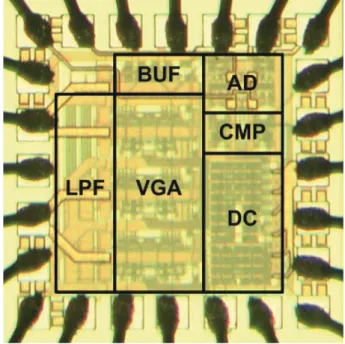
Fig. 9 shows the chip micrograph. Fabricated in a generic 0.18 μm CMOS technology, the chip size is 0.62 by 0.62 mm2.
The total power dissipation is 84 mW from a 1.8 V supply.
V. CONCLUSION
This paper presents the design of an 8 Gbps automatic gain control (AGC) circuit to be applied in PAM receiver. To facilitate digital gain control and broadband operations, the variable gain amplifier (VGA) in the AGC loop is comprised of
nested-feedback transconducatnce and transimpedance amplifier, where the transconducatnce is digitally tuned for gain control. The output amplitude is rapidly captured by resettable peak and bottom hold detector and dual band low pass filter. With the proposed digital assisted gain control scheme, the locking time for the AGC loop is less than 200 ns.
ACKNOWLEDGMENT
The authors wish to thank chip implementation center (CIC) for chip fabrication.
REFERENCES
[1] S. Radovanoviü, A.J. Annema, and B. Nauta, “A 3-Gb/s Optical Receiver Front-end in 0.18ȝm CMOS,” IEEE J. Solid-State Circuits, vol. 40, no. 8, pp. 1706-1717, Aug. 2005.
[2] T. Ridder, P. Ossieur, B. Baekelandt, C. Mélange, J. Bauwelinck, C. Ford, X. Z. Qiu, and J. Vandewege, “A 2.7V 9.8Gb/s Burst-Mode TIA with Fast Automatic Gain Locking and Coarse Threshold Extraction,” IEEE ISSCC Dig. Tech. Papers, pp. 220-221, Feb. 2008.
[3] J. M. Khoury, “On the design of constant settling time AGC circuits,” IEEE Transactions on Circuits and Systems (II), vol. 45, pp. 283Ω294, Mar. 1998.
[4] W.-Z. Chen, R.-M. Gan, and S.-H. Huang, ”A Single Chip 2.5 Gbps CMOS Burst Mode Optical Receiver”, IEEE Transactions on Circuits and Systems (I), Oct. 2009.
[5] C.-F. Liao and S.-I. Liu, “A 10Gb/s CMOS AGC Amplifier with 35dB Dynamic Range for 10Gb Ethernet,” IEEE ISSCC Dig. Tech. Papers, pp. 2092–2101, Feb. 2006.
Fig. 8 Measured settling behavior of the AGC.