國 立 交 通 大 學
電子工程學系 電子研究所
博 士 論 文
氮氧化層及高介電常數介電層
在金氧半元件及快閃記憶體上之特性研究
Investigation of Nitrided Oxides and High-
κ
Dielectrics on MOS Devices and Flash Memories
研 究 生:陳永裕 Yeong-Yuh Chen
指導教授:羅正忠 博士 Dr. Jen-Chung Lou
簡昭欣 博士 Dr. Chao-Hsin Chien
氮氧化層及高介電常數介電層
在金氧半元件及快閃記憶體上之特性研究
研究生 : 陳永裕 指導教授 : 羅正忠 博士 簡昭欣 博士 國立交通大學 電子工程學系 電子研究所 摘要 隨著系統晶片(SOC)的發展,持續降低 CMOS 元件中的閘極介電層及非 揮發性記憶體中的複晶矽層間介電層(inter-poly dielectric)厚度以提高元件密度 及降低操作電壓變得十分重要。為了滿足以上的需求並獲得較低的漏電流及較高 的可靠度,利用氮氧化層(nitrided oxide)及高介電常數材料(high-κ)來取代 二氧化矽變成是不可或缺的趨勢。 本篇論文首先研究利用成長氧化層前的氮原子離子佈植(nitrogen-implanted Si substrate)及氧化層成長後的一氧化氮(NO)高溫退火來改善傳統二氧化矽閘 極介電層的可靠度。其次,經由模擬工具將高介電常數材料做為堆疊式快閃記憶 體(stacked-gate flash memory)的複晶矽層間介電層和穿隧介電層(tunneldielectric),並討論其對快閃記憶體寫入/抹除的效率。最後,探討表面氨氣(NH3)
氮化處理及沉積後高溫退火(post-deposition annealing)溫度對反應式濺鍍 (reactive sputtering)及有機金屬化學氣相沉積(metal organic chemical vapor
deposition)之高介電常數材料三氧化二鋁(Al2O3)及二氧化鉿(HfO2)複晶矽 層間電容的影響。 首先,研究利用成長氧化層前的氮原子離子佈植及氧化層成長後的一氧化 氮高溫退火來改善傳統二氧化矽閘極介電層的可靠度。研究結果顯示成長後的一 氧化氮高溫退火會在界面處造成氮原子聚集,而成長氧化層前的氮原子離子佈植 則會造成氮原子均勻分布在氮氧化層裡。摻雜進入氧化層的氮濃度也會隨著氧化 層厚度而變;氧化層厚度愈薄,氮濃度愈高。聚集在界面處的氮原子有助於增強 二氧化矽介電層的可靠度,包括較平整的界面、較小的電洞捕捉(hole trapping)、 改善崩潰時間(time-to-breakdown)及崩潰電荷(charge-to-breakdown)等。此 外,介電層的可靠度還可由氮離子佈植濃度決定。當濃度小於 1×1014 cm-2時, 氧化速率不但不會降低,還會造成介電層可靠度劣化;相反的,若將濃度提高至 1×1015 cm-2,氧化速度可以很明顯的被抑制並用來成長多種不同介電層厚度以滿 足系統晶片需求,還可同時改善介電層可靠度。配合成長氧化層前的氮原子離子 佈植和氧化層成長後的一氧化氮高溫退火更可大幅提高閘極介電層的可靠度,用 以取代 0.13 微米以下製程的二氧化矽閘極介電層。 其次,經由模擬工具將高介電常數材料做為堆疊式快閃記憶體的複晶矽層 間介電層和穿隧介電層,並討論其對快閃記憶體寫入/抹除的效率。模擬結果指 出利用高介電常數材料取代傳統堆疊式快閃記憶體中的氧化層-氮化層-氧化 層(oxide-nitride-oxide)複晶矽層間介電層可明顯的提高寫入/抹除的速度,且 寫入/抹除的速度在 Fowler-Nordheim 穿隧上比熱電子(hot electron)注入的方 式更有效。選擇二氧化鉿做為複晶矽層間介電層並採用 Fowler-Nordheim 穿隧來 寫入/抹除,可大幅降低外加電壓達 48%。然而,高介電常數材料在穿隧介電層 上的應用結果卻截然相反。由於採用高介電常數材料做為穿隧介電層會降低閘極
的電壓藕合率(gate coupling ratio),利用 Fowler-Nordheim 穿隧反而會劣化寫入
電層的電場還低,但較低的電子位障高(barrier height)及增強的碰撞游離發生 率(impact ionization rate)卻使得高介電常數穿隧介電層在熱電子注入方式下有 較快的寫入/抹除速度。由於適用的寫入/抹除方式不同,高介電常數材料複晶 矽層間介電層及穿隧介電層可分別應用於 NAND 和 NOR 型式的堆疊式快閃記憶 體。 最後,探討表面氨氣氮化處理及沉積後高溫退火溫度對反應式濺鍍及有機 金屬化學氣相沉積之高介電常數材料三氧化二鋁及二氧化鉿複晶矽層間電容的 影響。表面氮化處理和高溫退火溫度都會造成反應式濺鍍的三氧化二鋁複晶矽層 間電容的特性和電壓極性相關。表面氮化處理會在界面處形成薄 Si-N 界面層, 抑制低介電常數界面層成長、形成較平滑的界面並讓後續的高溫退火更有效率的 消除原本存在的缺陷,得到較低的漏電流、較大的崩潰電場、較小的電子捕捉率 和較大的崩潰電荷。再者,反應式濺鍍的三氧化二鋁複晶矽層間電容的特性也受 高溫退火溫度影響甚巨。實驗結果顯示,不論是漏電流、電子捕捉率或崩潰電荷,
900oC 都是最佳化條件。根據 X 光光電子頻譜(X-ray photoelectron spectroscopy)
和 Auger 電子頻譜(Auger electron spectroscopy)的分析,發現溫度效應會造成 三氧化二鋁的組成比發生明顯的變化,其中氧原子的成份比將會決定複晶矽層間 介電層的特性。有鑑於反應式濺鍍的三氧化二鋁複晶矽層間電容的崩潰電荷過 低,我們也研究利用有機金屬化學氣相沉積方式沉積三氧化二鋁和二氧化鉿來改 善崩潰電荷的可能性。實驗結果證明,利用有機金屬化學氣相沉積除了可大幅改 善崩潰電荷外,也能有效的降低漏電流和增加崩潰電壓(breakdown voltage)和 有效崩潰電場(effective breakdown field)。因此,等效氧化層厚度為 5 奈米及 3 奈米的三氧化二鋁和二氧化鉿將是 45 奈米及 32 奈米世代以下堆疊式快閃記憶體 的絕佳候選複晶矽層間介電層。
Investigation of Nitrided Oxides and High-
κ Dielectrics
on MOS Devices and Flash Memories
Student : Yeong-Yuh Chen Advisors : Dr. Jen-Chung Lou Dr. Chao-Hsin Chien
Department of Electronics Engineering & Institute of Electronics National Chiao-Tung University
Abstract
For the system on a chip (SOC) application, a continuously scaling of the gate dielectrics for complementary metal oxide semiconductor (CMOS) and inter-poly dielectrics (IPDs) for electrically-erasable programmable read only memory (EEPROM) and stacked-gate flash memory is needed to obtain high density and low operation voltage. To meet the above requirements and exhibit a low leakage current and a good reliability, the replacement of nitrided oxides and high dielectric constant (high-κ) materials for the silicon dioxide (SiO2) and additional treatment have become
indispensable.
The first objective of this dissertation is to apply the pre-oxidation nitrogen implanted Si substrate (NIS) and post-oxidation nitric oxide (NO) annealing to improve reliabilities of conventional SiO2 gate dielectric. Then, investigates the
programming/erasing performances of stacked-gate flash memories through 2-D Medici simulation. Finally, the surface NH3 nitridation and post-deposition annealing
(PDA) temperature effects of the reactive-sputtered (RS) and metal organic chemical vapor deposition (MOCVD) high-κ IPDs is studied.
Firstly, we focused on the dielectric characteristics and reliability phenomena of NIS nitrided oxides with NO- and N2-annealing comparing to conventional SiO2 gate
oxide. It was found that a nitrogen pile-up occurred near the interface after NO-annealing, while NIS produced a uniform nitrogen distribution in the dielectric bulk. Incorporated nitrogen atomic concentration is also affected on the initial oxide thickness; thinner oxide thickness, higher nitrogen atomic concentration. Nitrogen pile-up near the interface is beneficial to enhance dielectric reliabilities in terms of smoothen interface roughness, reduced hole trapping, improved time-to-breakdown (tBD) and charge-to-breakdown (QBD). Moreover, it was found that the dielectric
reliability is strongly dependent on the NIS dosage. NIS with a dosage smaller than 1×10¹⁴
cm-2 is found to be useless in the oxidation rate suppression but degrades dielectric reliability simultaneously. On the contrary, the samples with 1×10¹⁵
cm-2 NIS dosage not only exhibit a significantly reduced oxidation rate, which can be used to grow multiple oxide thicknesses to meet the SOC requirement, but also improve stress immunity. NIS nitrided oxides with NO-annealing depict superior dielectric reliability and this technique appears suitable to replace the traditional SiO2 at 0.13
µm technology node and beyond.
Secondly, the effects of high-κ IPDs and TDs on a flash memory performance will be presented. By 2-D MEDICI simulation, flash memories with high-κ IPDs clearly exhibit significant improvement in programming/erasing speed over those with conventional ONO IPD. Moreover, it is found that high-κ IPDs are more effective for
the memories programmed/erased with Fowler-Nordheim (FN) tunneling rather than channel hot electron (CHE) injection. Choosing HfO2 as the IPD and using F-N
programming/erasing scheme, the operating voltage can be reduced 48% at a typical program time of 10 µs and 0.1 ms erasing time. Our results also show that dielectrics with very high permittivity (κ > 25) may not be necessary for the IPD in stacked-gate flash memories. On the other hand, the effect of high-κ TDs is quite contrary to the high-κ IPDs. Due to the reduced gate coupling ratio, the programming/erasing speed of stacked-gate flash memories with high-κ TDs by using FN tunneling is helpless in operation voltage reduction. Although the electric field on high-κ tunnel dielectrics is lower than SiO2 tunnel oxide, enhanced impact ionization rate and lower barrier
height contribute to higher CHE injection current and efficiency. Consequently, high-κ TDs are only effective for the memories programmed/erased with hot electron injection rather than FN tunneling. Due to the contrary programming/erasing schemes, high-κ IPDs and TDs are suitable for NAND- and NOR-type stacked-gate flash memories, respectively.
Finally, the effects of surface NH3 nitridation of the bottom poly-Si film and
PDA temperature on the electrical properties and reliability characteristics of RS and MOCVD high-κ inter-poly capacitors were evaluated. The polarity-dependent dielectric properties of RS Al2O3 IPD were strongly affected by the surface nitridation
and the annealing temperature. For positive gate bias, IPD with NH3 surface
nitridation were found to significantly suppress the formation of an additional layer with lower dielectric constant during the post-annealing process and obtain a smoother interface, compared to those without nitridation treatment. Furthermore, the presence of a thin Si-N layer can make PDA more effective in eliminating traps existing in the as-deposited films and improve dielectric characteristics under negative
polarity. As a result, the smoother interface and smaller electron trapping rate contribute to the drastically reduced leakage current, enhanced breakdown field, and QBD of the RS Al2O3 inter-poly capacitors with surface NH3 nitridation. Moreover,
the electrical properties of RS Al2O3 IPD are heavily dependent upon the PDA
temperature. The sample exhibits optimal quality in terms of leakage current, electron trapping rate and QBD when annealed at 900°C. X-ray photoelectron spectroscopy and
Auger electron spectroscopy analyses have shown that this occurrence arises from the composition variations under different annealing conditions and excess oxygen, which can act as an electron trapping center, playing an important role in determining the IPD electrical properties. The results apparently demonstrate Al2O3 IPD with surface
nitridation and optimized PDA temperature can effectively reduce charge transfer between CG and FG, better retention and disturb characteristics are expected by replacing ONO IPD to Al2O3 IPD. MOCVD Al2O3 and HfO2 IPD are investigated in
order to further promote QBD of RS Al2O3 IPD. The QBD can be significantly
improved as well as reduced leakage current density, enhanced breakdown voltage and effective breakdown field by using MOCVD replacing RS. As thin as 5nm and 3nm EOT of Al2O3 and HfO2 IPD is suitable to meet the requirement of 45nm and
Acknowledgements
There are many people to whom I owe a special word of thanks for their help to make my graduate studies possible. First, I would like to extend my sincere appreciation to Professor Jen-Chung Lou and Dr. Chao-Hsin Chien, my research advisors, for their guidance and assistance enabled the completion of this research. I am most grateful to them for providing me considerable freedom in directing my research. I would also like to thank Dr. Jeng Gong, Dr. Jenn-Gwo Hwu, Dr. Shui-Jinn Wang, Dr. Kwo-Ming Chang, Dr. Ming-Jer Chen, Dr. Tseung-Yuen Tseng and Dr. Bing-Yue Tsui for reading this thesis and serving on my oral examination committee. I am grateful to them for giving valuable criticism and suggestions for improving the exposition of the material in this dissertation.
I am indebted to the many professional and friendly staff members in National Nano-Devices Laboratories. I would like to thank my classmates Dr. Ching-Wei Chen, Mr. Wen-Tai Lu and junior classmates Mr. Shin-Chang Chen, Mr. Yen-Ting Chen and Mr. Tsung-Han Li for their useful discussions and suggestions. Special appreciation is also extended to Mei-Ling Fan and her parents, brother and sister for their kindly supported and encouraged me.
Finally, I would like to express my greatest appreciation to my parents, brother and sister who have supported and encouraged me through the years. Their love has always been the motive power to make me move forward and stay positive.
Contents
Abstract (in Chinese) ... I Abstract (in English) ... IV Acknowledgements ... VIII Contents ... IX Table Captions ... XIII Figure Captions ... XV
Chapter 1 Introduction ... 1
1.1 Background ... 1
1.2 Motivation ... 4
1.3 Organization of the Dissertation ... 6
Chapter 2 Characteristics and Reliabilities of Sub-3nm High Temperature NO-Annealed Nitrided Oxides ... 11
2.1 Introduction ... 11
2.2 Experimental Details ... 12
2.3 Results and Discussions ... 13
2.3.1 Accurate Models for Oxide Thickness Extraction ... 13
2.3.1.1 Corrected Two-Frequency Method for High Leakage Dielectrics ... 13
2.3.1.2 Quantum Confinement Effect Correction ... 14
2.3.1.3 Extract Tox using Accumulation Direct-Tunneling Currents ... 16
2.3.2 Basic Characteristics of Sub-3nm NO-Annealed Nitrided Oxides ... 17 2.3.3 Reliability Characteristics of Sub-3nm NO-Annealed Nitrided
Oxides ... 18
2.4 Summary ... 20
Chapter 3 Characteristics and Reliabilities of Sub-3nm Nitrided Oxides with Nitrogen-Implanted Silicon Substrates ... 33
3.1 Introduction ... 33
3.2 Experimental Details ... 34
3.3 Results and Discussions ... 35
3.3.1 Basic Characteristics of Sub-3nm NIS Nitrided Oxides ... 35
3.3.2 Reliability Characteristics of Sub-3nm NIS Nitrided Oxides ... 37
3.4 Summary ... 40
Chapter 4 Simulated Characteristics of Stacked-gate Flash Memories with Inter-Poly High-κ Dielectrics ... 53
4.1 Introduction ... 53
4.2 Simulation Details ... 54
4.3 Results and Discussions ... 55
4.3.1 Basic Characteristics of Flash Memories with High-κ IPDs and SiO2 TOX ... 55
4.3.2 Program/Erase Characteristics of Flash Memories with High-κ IPDs and SiO2 TOX ... 58
4.4 Summary ... 61
Chapter 5 Simulated Characteristics of Stacked-Gate Flash Memories with HfO2 IPD and High-κ Tunnel Dielectrics ... 73
5.2 Simulation Details ... 74
5.3 Results and Discussions ... 75
5.3.1 Basic Characteristics of Flash Memories with HfO2 IPD and High-κ TDs ... 75
5.3.2 Program/Erase Characteristics of Flash Memories with HfO2 IPD and High-κ TDs ... 76
5.4 Summary ... 79
Chapter 6 Study of Surface NH3 Nitridation on the Trapping Characteristics and Dielectric Reliabilities of Al2O3 IPD ... 89
6.1 Introduction ... 89
6.2 Experimental Details ... 91
6.3 Results and Discussions ... 92
6.3.1 Investigation of Surface NH3 Nitridation Effects on the RS Al2O3 IPD .. 92
6.3.2 Conduction Mechanism of the RS Al2O3 IPD ... 95
6.3.3 Polarity Dependence of the RS Al2O3 IPD ... 96
6.4 Summary ... 98
Chapter 7 Effects of PDA Temperature on the Electrical Properties of Al2O3 IPD with NH3 Nitridation ... 109
7.1 Introduction ... 109
7.2 Experimental Details ... 110
7.3 Results and Discussions ... 111
7.3.1 The Effects of Post-Deposition Temperature Annealing on the RS Al2O3 IPD ... 111
7.3.3 Physical Evidences of the Optimized 900oC PDA ... 116
7.4 Summary ... 119
Chapter 8 Thickness Scaling and Reliability Improvement of High-κ IPD for Next Decade Stacked-Gate Flash Memories ... 131
8.1 Introduction ... 131
8.2 Experimental Details ... 132
8.3 Results and Discussions ... 133
8.4 Summary ... 135
Chapter 9 Conclusions and Recommendations for Future Works ... 139
9.1 Conclusions ... 139
9.2 Recommendations for Future Works ... 142
References ... 143
Vita ... 157
Table Captions
Chapter 1
Table 1.1 Materials properties of high-κ dielectrics, Al2O3, ZrO2 and HfO2.
Chapter 2
Table 2.1 Comparison of thickness extraction from various methods of NO-annealed and N2-annealed GOX.
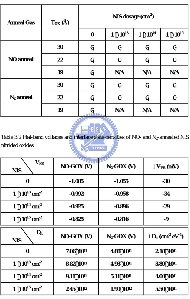
Table 2.2 Flat-band voltages and interface state densities of NO- and N2-annealed
GOX.
Chapter 3
Table 3.1 Experimental conditions of nitrided gate oxides formed by pre-oxidation NIS and post-oxidation NO-annealing.
Table 3.2 Flat-band voltages and interface state densities of NO- and N2-annealed
NIS nitrided oxides.
Table 3.3 Thickness and dielectric constant variation for NO- and N2-annealed NIS
nitrided oxides.
Chapter 4
Table 4.1 Dielectric constants and conduction band offsets with respect to Si of the IPD materials with fixed SiO2 TOX for simulated stacked-gate flash
memories.
Table 4.2 Operation voltage reduction of stacked gate flash memories with high-κ IPDs and SiO2 TOX.
Table 5.1 Dielectric constants and conduction band offsets with respect to Si of the TD materials with fixed HfO2 IPD for simulated stacked-gate flash
memories.
Table 5.2 Operation voltage reduction of stacked gate flash memories with HfO2 IPD
and high-κ TDs.
Chapter 6
Table 6.1 EOT, Poly-I surface roughness and 63%-failure QBD values of the
800oC-annealed Al2O3 inter-poly capacitors with and without surface NH3
nitridation.
Chapter 7
Table 7.1 EOT, Poly-I surface roughness and 63%-failure QBD values of the Al2O3
inter-poly capacitors with surface NH3 nitridation under positive and
negative CCS at various PDA temperatures in O2 ambient. Due to the
extremely large leakage current, the corresponding EOT and 63%-failure QBD values of the as-deposited Al2O3 inter-poly capacitors can not be
determinable.
Table 7.2 κ-value, interfacial layer thickness and extracted barrier heights of the Al2O3 inter-poly capacitors with surface NH3 nitridation at various PDA
temperatures in O2 ambient.
Chapter 8
Table 8.1 Deposition conditions and EOT of the various IPDs deposited either by LPCVD, RS or MOCVD.
Table 8.2 Breakdown voltage, effective breakdown field and 63%-failure QBD values
Figure Captions
Chapter 1
Fig. 1.1 Scaling limits of various gate dielectrics as a function of the technology specifications for low stand-by power technologies.
Fig. 1.2 Leakage current density and EOT projection of nitrided oxides from ITRS roadmap 2003.
Chapter 2
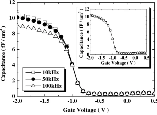
Fig. 2.1 The C-V curves of the 19Å NO-annealed GOX. Inset shows corrected C-V curves by two-frequency method.
Fig. 2.2 Extracted dielectric constants of NO- and N2-annealed GOX. NO-annealed
GOX has higher dielectric constant than N2-annealed GOX.
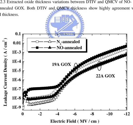
Fig. 2.3 Extracted oxide thickness variations between DTIV and QMCV of NO- and N2-annealed GOX. Both DTIV and QMCV thickness show highly
agreement with TEM thickness.
Fig. 2.4 Direct tunneling current density of 19Å and 22Å NO- and N2-annealed
GOX. NO-annealing does not deteriorate leakage current.
Fig. 2.5 (a) Normalized C-V curves of 19Å and 22Å NO- and N2-annealed GOX.
(b) Magnify (a) for clearly comparison between NO- and N2-annealed
GOX. NO-annealing exhibits negative flat-band voltage shift and slightly increases interface state density.
Fig. 2.6 (a) XPS nitrogen depth profiles (b) nitrogen peak concentrations of NO-annealed nitrided oxides varied with initial oxide thickness. NO-annealing piles-up nitrogen near the interface and more N incorporates as oxide thickness decreasing.
Fig. 2.7 SILC characteristics of 19Å NO- and N2-annealed GOX at -3.8V CVS for
100sec. Maximum current increment after CVS occurs near flat band region.
Fig. 2.8 (a) SILC characteristics (b) transient hole-trapping behavior of 22Å NO- and N2-annealed GOX at -4V CVS. NO-annealing can suppress both
hole-trapping and maximum trap generation rate occurred near flat-band region during constant voltage stress.
Fig. 2.9 Maximum trap generation rate of 22Å N2- and NO-annealed GOX stressed 2
NO-annealing can reduce hole-trap generation rate during both voltage and current stress.
Fig. 2.10 (a) TDDB Weibull plots of 19Å and 22Å N2- and NO-annealed GOX at
-4.3V CVS. (b) QBD Weibull plots of 22Å N2- and NO-annealed GOX at
-20 mA/cm2 CCS. NO-annealed nitrided oxides exhibits higher stress immunity than N2-annealed oxides.
Fig. 2.11 The HRTEM cross-sectional images of 22Å (a) N2- and (b) NO-annealed
GOX. NO-annealing has smoother interface than N2-annealing.
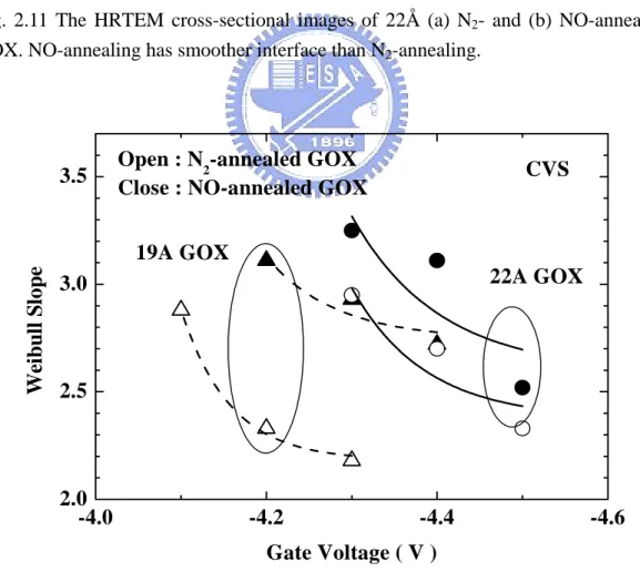
Fig. 2.12 Plots of weibull slope of 19Å and 22Å N2- and NO-annealed GOX.
NO-annealing clearly enhances Weibull slope.
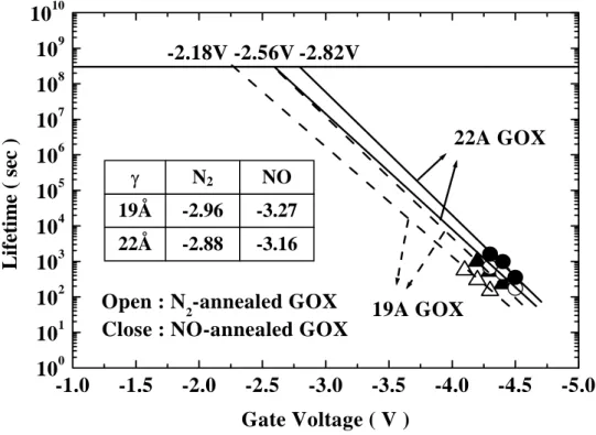
Fig. 2.13 10-year lifetime projection of 19Å and 22Å N2- and NO-annealed GOX.
Inset also indicates voltage acceleration factors.
Chapter 3
Fig. 3.1 Plots of high frequency C-V curves of 22Å (a) N2-annealed (b)
NO-annealed NIS nitrided oxides. Significant oxidation rate retardation is inspected as NIS dosage larger than 1×10¹⁴
cm-2. As NIS dosage larger than 1×10¹⁵
cm-2, clear VFB shift and Dit increment is observed.
Fig. 3.2 (a) Oxide thickness (b) dielectric constant as a function of nitrogen dosage implanted into the silicon substrate before oxidation. Dielectric constant increases from 3.9 to 4.6 for NO-annealed NIS nitrided oxides with heavy implantation dosage.
Fig. 3.3 Direct tunneling leakage current density as a function of gate voltages of 22Å (a) N2-annealed (b) NO-annealed NIS nitrided oxides. Direct
tunneling leakage current density is strongly dependent on the dosage of nitrogen implanted into Si substrate..
Fig. 3.4 (a) XPS depth profiles of 22Å NO-annealed nitrided oxides with 4×1015 cm-2 NIS. Evidence of Si3N4-like interface is observed. (b) SIMS nitrogen
depth profiles of 30Å NO-annealed NIS nitrided oxides. NIS incorporates uniform nitrogen distribution in the bulk.
Fig. 3.5 SILC characteristics of 22Å (a) N2-annealed (b) NO-annealed NIS nitrided
oxides at -4V CVS for 100sec. Maximum current increase after CVS occurs near flat band region. Increased SILC is negligible for 1×10¹⁵
cm-2 NIS nitrided oxides.
Fig. 3.6 (a) Transient hole-trapping behaviors (b) maximum trap generation rates of 22Å NO-annealed NIS nitrided oxides at -20 mA/cm2 constant current stress. NIS nitrided oxides with 1×10¹⁵
generation rate for both CVS and CCS.
Fig. 3.7 (a) tBD Weibull distribution (b) Weibull slopes of 22Å NO-annealed NIS
nitrided oxides under -4.3V constant voltage stress. The reliability of NIS nitrided oxides is substantially relied on NIS dosage, tBD and Weibull slope
are increased only for NIS nitrided oxides with 1×10¹⁵
cm-2 dosage.
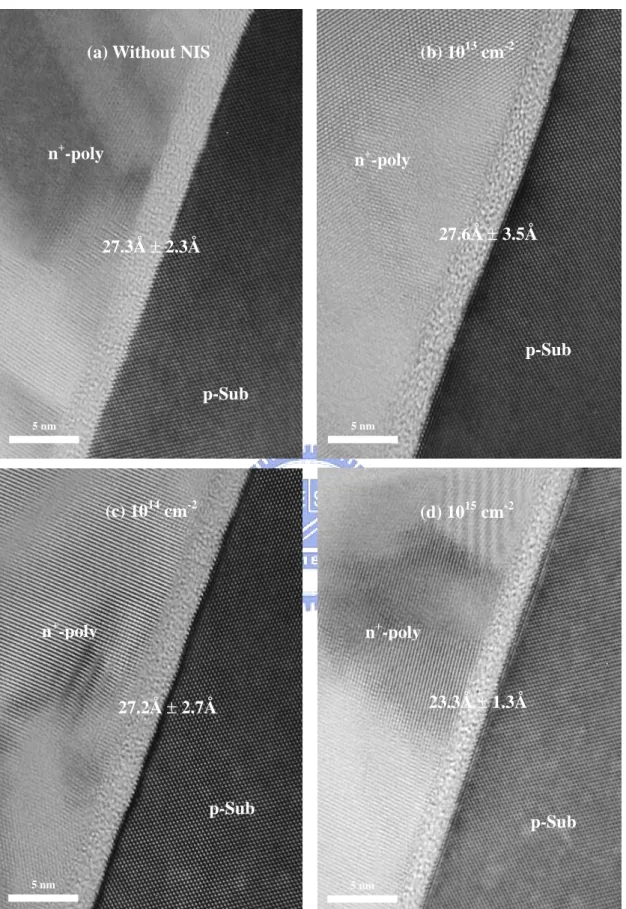
Fig. 3.8 The HRTEM cross-sectional images of 22Å N2-annealed NIS nitrided
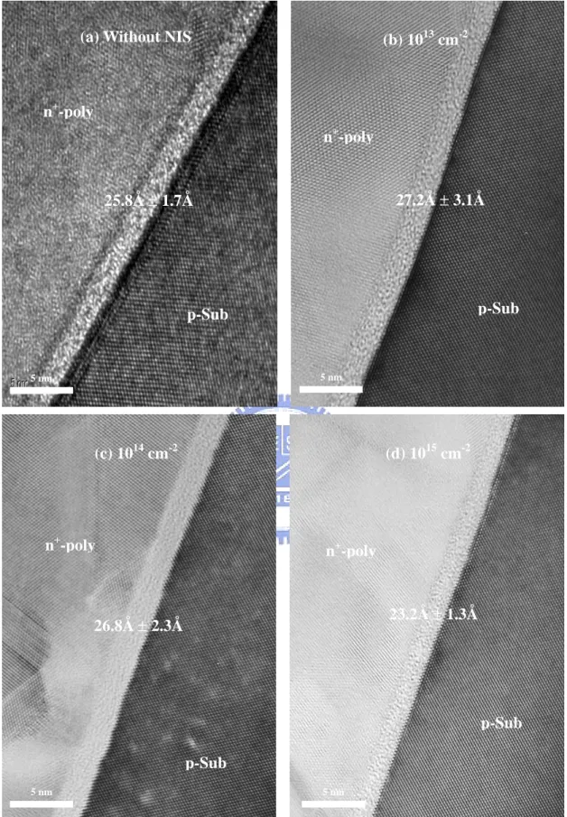
oxides. (a) without NIS (b) 1013 cm-2 (c) 1014 cm-2 (d) 1015 cm-2. Sample with 1015 cm-2 NIS not only smoothes interface but also reduces physical thickness.
Fig. 3.9 The HRTEM cross-sectional images of 22Å NO-annealed NIS nitrided oxides. (a) without NIS (b) 1013 cm-2 (c) 1014 cm-2 (d) 1015 cm-2. Sample with 1015 cm-2 NIS not only smoothes interface but also reduces physical thickness.
Fig. 3.10 Substrate surface roughness of NO-annealed NIS nitrided oxides after dielectrics removal by diluted HF solution. Evidence of smooth interface is revealed for samples with 1015 cm-2 NIS and post-oxidation NO annealing.
Chapter 4
Fig. 4.1 (a) Simulated 0.45µm n-channel device structure (b) equivalent electrical model of stacked-gate flash memories with several high-κ IPDs and TDs. Asymmetry source/drain junction for enhanced source-side erasing efficiency. Programming by either CHE or CFN injection; erasing by SFN erasing.
Fig. 4.2 (a) IPD (b) TOX electric field as a function of control gate voltages of erased state stacked-gate flash memories with high-κ IPDs and SiO2 TOX
under VD = VB = VS = -9.0V. High-κ IPDs can reduce IPD electric field as
well as enhance TOX electric field.
Fig. 4.3 (a) Linear region (b) saturation region transfer characteristics of stacked-gate flash memories with high-κ IPDs and SiO2 TOX. High-κ
IPDs can increase drive-in current as well as enhance gate control ability, especially at high drain voltage.
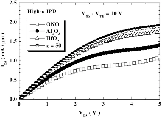
Fig. 4.4 Output characteristics of stacked-gate flash memories with high-κ IPDs and SiO2 TOX at (VGS - VTH) = 10V.
Fig. 4.5 Substrate current of stacked-gate flash memories with high-κ IPDs and SiO2 TOX. Maximum substrate current is independent of the κ-values.
memories with high-κ IPDs and SiO2 TOX. High-κ IPDs slightly enhance
injection efficiency than ONO IPD, but not significantly.
Fig. 4.7 CHE programming time as a function of control gate voltages of stacked-gate flash memories with high-κ IPDs and SiO2 TOX.
Fig. 4.8 CFN current injected to FG as a function of control gate voltages of stacked-gate flash memories with high-κ IPDs and SiO2 TOX.
Fig. 4.9 CFN programming time as a function of control gate voltages of stacked-gate flash memories with high-κ IPDs and SiO2 TOX. Significant
improvement in CFN programming speed for high-κ IPDs is indicated. Fig. 4.10 (a) Absolute IPD (b) TOX electric field as a function of control gate
voltages of programmed state stacked-gate flash memories with high-κ IPDs and SiO2 TOX under VS = 5.0V. Drain and substrate terminals are
floating. High-κ IPDs can reduce IPD electric field as well as enhance TOX electric field.
Fig. 4.11 Band diagrams of programmed state flash memories at the outset of erase for (a) high-κ IPDs and (b) ONO IPD.
Fig. 4.12 SFN current ejected from FG of stacked-gate flash memories with high-κ IPDs and SiO2 TOX under VS = 5.0V, floated drain and substrate terminal.
Fig. 4.13 SFN erasing time of stacked-gate flash memories with high-κ IPDs and SiO2 TOX. High-κ IPDs crucially improve SFN erasing speed.
Chapter 5
Fig. 5.1 (a) IPD (b) TD electric field as a function of control gate voltages of erased state stacked-gate flash memories with HfO2 IPD and high-κ TDs under
VD = VB = VS = -9.0V. High-κ TDs can increase IPD electric field as well
as reduce TD electric field.
Fig. 5.2 (a) Linear region (b) saturation region transfer characteristics of stacked-gate flash memories with HfO2 IPD and high-κ TDs. The flash
memories with HfO2 IPD and high-κ TDs not only depict the degraded subthreshold swing but also exhibit significantly large off-state current. Fig. 5.3 Output characteristics of stacked-gate flash memories with HfO2 IPD and
high-κ TDs.
Fig. 5.4 Substrate current of stacked-gate flash memories with HfO2 IPD and
high-κ TDs. Maximum substrate current is substantially dependent of the κ-values of TDs.
of control gate voltages of stacked-gate flash memories with HfO2 IPD and
high-κ TDs at VDS = 5.0V. Flash memories with high-κ TDs dramatically
enhance injection efficiency than SiO2 TOX.
Fig. 5.6 CHE programming time as a function of control gate voltages of stacked-gate flash memories with HfO2 IPD and high-κ TDs at VDS = 5.0V.
Fig. 5.7 CFN current injected to FG as a function of control gate voltages of stacked-gate flash memories with HfO2 IPD and high-κ TDs at VDS = 5.0V.
Fig. 5.8 CFN programming time as a function of control gate voltages of stacked-gate flash memories with HfO2 IPD and high-κ TDs at VD = VB =
VS = -9.0V. Obvious degradation in CFN programming speed for high-κ
TDs is indicated.
Fig. 5.9 (a) Absolute IPD (b) TD electric field as a function of control gate voltages of programmed state stacked-gate flash memories with HfO2 IPD and
high-κ TDs under VS = 5.0V. Drain and substrate terminals are floating.
High-κ TDs would increase IPD electric field as well as reduce TD electric field.
Fig. 5.10 SFN current ejected from FG of stacked-gate flash memories with HfO2
IPD and high-κ TDs under VS = 5.0V, floated drain and substrate terminal.
Fig. 5.11 SFN erasing time of stacked-gate flash memories with HfO2 IPD and
high-κ TDs. High-κ TDs crucially deteriorate SFN erasing speed.
Chapter 6
Fig. 6.1 Cross-sectional view of Al2O3 inter-poly capacitor with surface NH3
nitridation and post-deposition oxygen annealing.
Fig. 6.2 Key process steps of Al2O3 inter-poly capacitor with surface NH3
nitridation and post-deposition oxygen annealing.
Fig. 6.3 (a) J-E characteristics (b) C-V curves of 800oC-annealed Al2O3 inter-poly
capacitors with and without surface NH3 nitridation under both polarities.
Surface nitridation is beneficial in thinning EOT and lowering leakage current density compared to samples without nitridation.
Fig. 6.4 High resolution TEM images of Al2O3 inter-poly capacitors after 800oC
annealing (a) with (b) without surface NH3 nitridation. Physical thickness
of Al2O3 IPD is estimated to be 8.5 nm. Samples with NH3 nitridation
can effectively reduce interfacial layer growth and smooth interface roughness.
Fig. 6.5 Leakage current density Weibull distributions at 3 MV/cm and 8 MV/cm
nitridation under (a) positive VG (b) negative VG. Surface NH3 nitridation
can effectively reduce low and high field leakage current under both polarities.
Fig. 6.6 Effective breakdown field Weibull distributions of 800oC-annealed Al2O3
inter-poly capacitors with and without NH3 nitridation in both polarities.
Fig. 6.7 Dielectric relaxation current of 800oC-annealed Al2O3 inter-poly capacitors
with and without NH3 nitridation in both polarities.
Fig. 6.8 (a) Curves of gate voltage shift (b) QBD Weibull plots of Al2O3 inter-poly
capacitors after 800oC annealing with and without surface NH3 nitridation
under constant current stress. Samples with NH3 nitridation can suppress
electron-trapping generation and increase QBD.
Fig. 6.9 (a) Measuring temperature dependence of leakage current density (b) Fowler-Nordheim tunneling fitting of Al2O3 inter-poly capacitors after
800oC annealing with and without surface NH3 nitridation.
Fig. 6.10 AFM images (5µm×5µm) of the poly-I surface before Al2O3 IPD
deposition (a) with (b) without surface NH3 nitridation, and after 800°C
O2 annealing (c) with (d) without surface NH3 nitridation. Surface
nitridation can eliminate surface roughness apparently.
Fig. 6.11 AES depth profiles of Al2O3 inter-poly capacitors after 800oC annealing
with and without surface NH3 nitridation. Surface nitridation clearly
suppresses interfacial Al, O and Si inter-diffusion.
Chapter 7
Fig. 7.1 (a) C-V curves (b) J-E characteristics of Al2O3 inter-poly capacitors with
surface NH3 nitridation annealed at 800oC to 1000oC in O2 ambient. Al2O3
inter-poly capacitor with 900oC PDA in O2 ambient is beneficial in scaling
EOT and suppressing low-field leakage current density.
Fig. 7.2 (a) As-fabrication trap densities evaluation at 2 MV/cm constant voltage stress (CVS) (b) dielectric relaxation current of Al2O3 inter-poly capacitors
with surface NH3 nitridation annealed at 800oC to 1000oC in O2 ambient.
Al2O3 inter-poly capacitor with 900oC PDA in O2 ambient can reduce
as-fabricated trap densities.
Fig. 7.3 (a) Curves of gate voltage shift (b) QBD Weibull plots of Al2O3 inter-poly
capacitors with surface NH3 nitridation annealed at 800oC to 1000oC in O2
ambient under constant current stress. Al2O3 inter-poly capacitors with
optimized 900oC PDA can suppress electron-trapping and increase QBD.
surface NH3 nitridation annealed at 800oC to 1000oC in O2 ambient.
Fig. 7.5 Temperature dependence of gate current density at 6 MV/cm of Al2O3
inter-poly capacitors with surface NH3 nitridation annealed at 800oC to
1000oC.
Fig. 7.6 (a) Centroid of trapped charges (b) trapped charge density of Al2O3
inter-poly capacitors with surface NH3 nitridation annealed at 800oC to
1000oC in O2 ambient under constant current stress. Al2O3 inter-poly
capacitors with optimized 900oC PDA can suppress electron trapping rate below 10-4.
Fig. 7.7 Band diagrams of Al2O3 inter-poly capacitors with surface NH3 nitridation
under (a) positive (b) negative gate voltage biased to the Poly-II. Al2O3
inter-poly capacitors at negative polarity show less electron trapping and gate voltage shift.
Fig. 7.8 (a) XPS binding energy spectrum (b) corresponding XPS binding energy spectrum after arranging to the equivalent background signal for the O 1s and Al 2p signals as a function of PDA temperatures with C 1s calibration at 284.5 eV. The binding energy of O and Al signals is strongly dependent on PDA temperature.
Fig. 7.9 Al and O atomic concentrations extracted from XPS as a function of PDA temperatures with C 1s calibration at 284.5 eV.
Fig. 7.10 Weibull plots of effective breakdown field of Al2O3 inter-poly capacitors
with surface NH3 nitridation annealed at 800oC to 1000oC in O2 ambient.
Fig. 7.11 AFM images (5µm×5µm) of the poly-I surface of Al2O3 inter-poly
capacitors with surface NH3 nitridation for (a) as-deposited (b) 800oC (c)
900oC (d) 1000oC PDA in O2 ambient. Surface roughness becomes more
severe as PDA temperature increasing.
Fig. 7.12 XRD spectra for aluminum oxide on Si(100). Al2O3 IPD is crystallized
while PDA temperature larger than 900oC.
Fig. 7.13 AES depth profiles of Al2O3 IPD with surface NH3 nitridation annealed at
800oC to 1000oC in O2 ambient. The signal of N is magnified by 5 times.
Chapter 8
Fig. 8.1 Current density at 5V as a function of EOT for various IPDs. High-κ IPDs can reduce leakage current larger than 1-order of magnitude.
Fig. 8.2 Breakdown voltage as a function of EOT for various IPDs. High-κ IPDs exhibits higher breakdown voltage than TEOS IPD.
Fig. 8.3 Effective breakdown field as a function of EOT for various IPDs. High-κ IPDs exhibits higher breakdown field than TEOS IPD.
Fig. 8.4 Charge-to-breakdown as a function of EOT for various IPDs. High-κ IPDs exhibits higher QBD than TEOS IPD.
CHAPTER 1
Introduction
1.1 Background
The rapid progress of complementary metal-oxide-semiconductor (CMOS) integrated circuit technology since the late 1980’s has enabled the Si-base microelectronics industry to simultaneously meet several technological requirements to fuel market expansion. These requirements include performance (speed), low static (off-state) power and a wide range of power supply and output voltages [1]. This has been accomplished by developing the ability to perform a calculated reduction of the dimensions of the fundamental active device in the circuit, following the “Moore’s law”, doubling about every two or three years since about 1980 [2]-[4]. The result has been a dramatic expansion in technology and communications markets including the market associated with high-performance microprocessors as well as low static-power applications, such as wireless systems.
It can be argued that the key element enabling the scaling of the Si-based metal-oxide-semiconductor field effect transistor (MOSFET) is the materials and resultant electrical properties associated with the dielectric employed to isolate the transistor gate from the Si channel for decades: silicon dioxide (SiO2). The use of
high-quality Si-SiO2 interface as well as superior electrical isolation properties. In
modern CMOS processing, defect charge densities are on the order of 1010 cm-2, midgap interface state densities are ~ 1010 cm-2eV-1 and hard breakdown fields of 15 MV/cm are routinely obtained and are therefore expected regardless of the device dimensions. These outstanding electrical properties clearly present a significant challenge for any alternative gate dielectric candidate [5], [6].
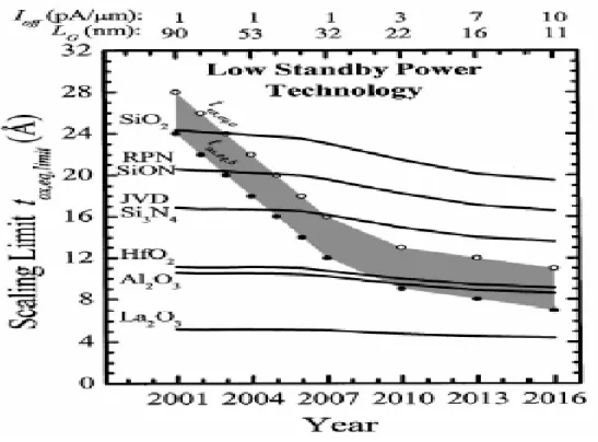
Over the years, there have been several major evolutions in silicon digital logic technology. CMOS technology has become the most popular digital logic technology for all IC industry, owing to its low standby power dissipation and scaling properties. Oxide thickness scaling has long been recognized as one of major keys for devices scaling. High drive current and thereby improved device performance can be achieved by reducing oxide thickness. It suggests that at the current rate of progress, Fig. 1.1 stresses the urgent need for a nitrided oxides (SiOxNy) and high dielectric constant (κ)
gate dielectrics for low stand-by power application after the year 2002 and 2006, respectively [7]. Besides, the direct tunneling current increases exponentially by about one order of magnitude for every 0.2nm ~ 0.3nm reduction in oxide thickness. This additional leakage current not only causes increased power dissipation but also may affect the circuit functionality due to the decreased operation margins.
For this reason, several alternative materials for silicon dioxide are currently being investigated. Ultrathin nitrided oxides are the leading candidates to replace pure SiO2 [8]-[14]. Figure 1.2 shows the expected equivalent oxide thickness (EOT) trends
from the published 2003- ITRS roadmap. It suggests nitrided oxides can extend SiO2
limitation to 2006 without massive change in production technologies.Nitrided oxides exhibit several properties superior to those of conventional thermal SiO2, the more
reliability. Nitrogen also reduces hot-electron-induced degradation [15]. The dielectric constant of the oxynitride increases linearly with the percentage of nitrogen from κ (SiO2) = 3.9 to κ (Si3N4) = 7.8 [16], though one should note that most SiOxNy films
grown currently by thermal methods are lightly doped with N (< 10 at.%) and therefore have a dielectric constant only slightly higher than that of pure SiO2. The
other potential candidates to replace silicon dioxide are high-κ materials, including aluminum oxide (Al2O3), hafnium oxide (HfO2) and zirconium oxide (ZrO2) etc
[17]-[20]. The most benefic for high-κ dielectrics is leakage current reduction by several orders of magnitude at the same EOT compared to SiO2. However, in device
performance point of view, a suitable gate dielectric candidate should also meet the other requirements, including high thermal stability, high carrier mobility, small oxide charges, good stress immunity and CMOS compatible.
On the other hand, high-κ dielectrics are paid much attention on the flash memory applications [21]-[27]. The thickness of inter-poly dielectric (IPD) and tunnel dielectric (TD) in stacked-gate flash memory had meet intrinsic limitation [28]. It is not sufficient to meet the stringent data retention requirement of IPD while applying thermal or CVD oxynitride technologies due to the unavoidable leakage current [29]-[32]. By increasing the floating gate coupling ratio, high-κ IPD can lead to a high electric field across tunnel oxide (TOX) even at very low control gate voltage. For the tunnel dielectric engineering of stacked-gate flash memories, the issue is closely related to dielectric material selection itself. Flash tunnel dielectric has two roles. One is a barrier to suppress charge leakage under read and retention. Second role is a charge transfer path. In order to avoid trap-assisted tunneling via one trap site, the minimum TOX thickness of conventional FG structure will be limit to 8 nm. This limits the tunnel SiO2 scaling and program/erase voltage reduction. Nitrided oxide
have been intensively studied, but so far only 5 to 10 times improvement for low field leakage is achieved [33]. This is not enough, because it only achieves 1 nm reduction even with heavy nitridation.
To successfully employ the high-κ IPD and TD into flash memory, one must take charge retention issues into consideration and make sure that the barrier height (ϕB) between Si and the new adopted high-κ dielectrics should be larger than 1.5eV
for effectively suppressing the loss of floating gate charges through electron thermal emission [33]. Usually, dielectrics with higher κ inherently have lower ϕB. Therefore
a trade-off between dielectric constant and barrier height is inevitably required in trying to implement the high-κ dielectrics in flash memories.
1.2 Motivation
Recent publications suggest that the performance of CMOS-based devices depends on both the concentration and distribution of the nitrogen atoms incorporated into the gate dielectric [9]-[11], [34]-[36]. For example, excessive nitrogen at the interface may reduce peak carrier mobility in the channel of MOSFETs and may allow boron accumulation in the oxide, which, in turn, may result in device instabilities [34]. One possibility is an SiOxNy film with two nitrogen-enhanced layers: first, nitrogen at
or near the Si/SiOxNy interface to improve hot-electron immunity, and second, an
even higher nitrogen concentration at the SiOxNy/polysilicon interface, as this is
where it can best be used to minimize the penetration of boron from the heavily doped p+ poly-gate electrode [37]. Thermal nitridation of SiO2 in nitric oxide (NO) or nitrous
[37]-[39]. Although N2O processing similarity to O2 permits N2O to replace oxygen in
oxidation reactors/furnaces, oxynitridation in N2O is complicated by the fast
gas-phase decomposition of the molecule into N2, O2, NO and O at typical oxidation
temperatures, 800 - 1100oC [13]. Therefore, NO-annealing of an initial oxide is preferred to prepare nitrided oxide with sufficient concentration in a reasonable thermal cycle [9], [14], [36], [39]. Compared to N2O, oxynitridation in NO results in
more nitrogen incorporation at equivalent temperatures [9], [40], [41]. In addition, NO oxynitrides exhibit lower leakage currents and interface defect densities, as well as improved electrical stress properties [9], [36], [40]. On the other hand, system-on-a-chip has gradually become the trend of CMOS technologies. As a result, circuit architecture and material reliability are both mixed into the design consideration. In these applications, minimizing process steps and forming thermally stable dual oxide thickness CMOSFETs are essential. One of the ways for reducing the number of process steps is to implant nitrogen into Si substrate in order to obtain two gate oxide thickness on the same thermal cycle [42], [43].
Recently, aluminum oxide (Al2O3) [17], [44]-[46] and hafnium oxide (HfO2)
[20], [47]-[50] had been proved as promising candidates for the gate dielectrics of sub-0.1 µm device due to their higher κ, relatively high ϕB and superior thermal
stability, shown in Table 1.1. Thanks to the high dielectric constant and high thermal stability, Al2O3 and HfO2 are suitable to be integrated into stacked-gate flash
memories. Nonetheless, the effects of these kinds of high-κ dielectrics on flash memories are seldom investigated. To further realize the dielectric properties of these high-κ dielectrics, some reliability issues such as breakdown field, charge trapping and temperature-dependence behaviors are extensively studied for both gate dielectric and flash memories applications.
1.3 Organization of the Dissertation
There are nine chapters in this dissertation. Chapter 1 shows the background and motivation for the application of the ultrathin nitrided oxides and high-κ dielectrics.
In Chapter 2, the reliabilities of sub-3nm nitrided oxides formed by NO-annealing are shown. In our study, N atomic concentration is shown to depend on the initial oxide thickness, i.e., concentration increases as oxide thickness decreases, which was desired for the improvement of dielectric reliability in the ultra-thin thickness region. NO-annealing can achieve better SILC immunity for both constant voltage and constant current stress. Moreover, NO-annealing also improves interface smoothness and results in tighter TDDB distribution.
In Chapter 3, the reliabilities of sub-3nm nitrided oxides formed by nitrogen-implanted silicon substrate (NIS) are investigated. NIS dosage less than 1×10¹⁴
cm-2 is helpless to oxidation rate suppression and degrades dielectric reliability simultaneously. On the contrary, samples with 1×10¹⁵
cm-2 NIS not only can use to grow multiple oxide thickness to meet SOC requirement, but also improve stress immunity apparently. Nitrogen implantation also generates a uniform distribution nitrogen profile in the dielectric bulk, which can be used as an effective diffusion barrier to resist boron penetration. In conclusion, both NO-annealed and NIS nitrided oxides can improve dielectric reliability and are suitable to replace traditional SiO2 at
0.13µm and beyond.
In Chapter 4, the program/erase performance of stacked-gate flash memory with high-κ IPDs and SiO2 TOX are compared to ONO IPD. From MEDICI simulation,
respectively. By 2-D MEDICI simulation, flash memories with high-κ IPD clearly exhibit significant improvement in programming/erasing speed over those with conventional ONO IPD. Moreover, it is found that high-κ IPD is more effective for the memories programmed/erased with Fowler-Nordheim (FN) tunneling rather than channel hot carrier (CHE) injection. Choosing HfO2 as the IPD and using FN
programming/erasing scheme, the operating voltage can be reduced 48% at a typical program time of 10 µs and 0.1 ms erasing time.
In Chapter 5, the program/erase performance of stacked-gate flash memory on the κ-value of tunnel dielectric are studied. The effect of high-κ TD is quite different with high-κ IPD. Due to the reduced gate coupling ratio, the programming/erasing speed of stacked-gate flash memories with high-κ TD by using FN tunneling is helpless in operation voltage reduction. On the other hand, the increased electric field on HfO2 IPD would produce excess charge loss and narrow the operation window
between programmed and erased state. Although the electric field on high-κ tunnel dielectrics is lower than SiO2 TOX, enhanced impact ionization rate and lower
electron barrier height contribute to higher CHE injection current and efficiency. Consequently, high-κ TD is more effective for the memories programmed/erased with hot electron injection rather than FN tunneling. Due to the contrary improvement in programming/erasing schemes, high-κ IPD and TD is suitable for next-generation NAND and NOR type stacked-gate flash memories, respectively.
In Chapter 6, the effects of surface ammonia (NH3) nitridation on inter-poly
characteristics of reactive-sputtered (RS) Al2O3 dielectrics are evaluated. With surface
NH3 nitridation, the formation of an additional layer with lower dielectric constant
during post-annealing process can be significantly suppressed and reduced, compared to that without nitridation treatment. Furthermore, the presence of a thin Si-N layer
can make post-deposition annealing more effective in eliminating traps existing in the as-deposited films. As a result, a smoother interface and smaller electron trapping rate can contribute to the drastically reduced leakage current, enhanced breakdown field and QBD of Al2O3 interpoly capacitors with surface NH3 nitridation for both polarities.
In Chapter 7, the effects of post-deposition annealing (PDA) temperature on inter-poly characteristics of RS Al2O3 dielectrics are examined. It was found that the
electrical properties of Al2O3 IPD strongly depend upon the PDA temperature. 900°C
annealing is the best condition for the Al2O3 IPD electrical characteristic in terms of
leakage current, electron trapping rate and charge-to-breakdown. The XPS and AES analyses indicate that this consequence is closely related to the compositional changes and excess oxygen concentration when changing annealing temperature. The results apparently demonstrate Al2O3 IPD with surface nitridation and optimized PDA
temperature can effectively reduce charge transfer between CG and FG, better retention and disturb characteristics are expected by replacing ONO IPD to Al2O3
IPD.
In Chapter 8, thickness scaling down and reliability promotion of next-decade suitable IPD are inspected. The results clearly indicates high-κ IPDs, regardless of deposition tools, exhibits high potential to replace TEOS IPD. Moreover, MOCVD deposition demonstrates significant reliability improvement compared to RS deposition. As thin as 5nm and 3nm EOT of MOCVD-deposited Al2O3 and HfO2 IPD
is suitable to meet the requirement of 45nm and 32nm generation stacked-gate flash memories, respectively.
Finally, in Chapter 9, the conclusions are made and the recommendation describes the topics which can be further researched.
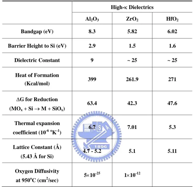
Table 1.1 Materials properties of high-κ dielectrics, Al2O3, ZrO2 and HfO2.
High-κ Dielectrics
Al2O3 ZrO2 HfO2
Bandgap (eV) 8.3 5.82 6.02
Barrier Height to Si (eV) 2.9 1.5 1.6
Dielectric Constant 9 ~ 25 ~ 25 Heat of Formation (Kcal/mol) 399 261.9 271 ∆G for Reduction (MOx + Si → M + SiOx) 63.4 42.3 47.6 Thermal expansion coefficient (10-6oK-1) 6.7 7.01 5.3 Lattice Constant (Å) (5.43 Å for Si) 4.7 - 5.2 5.1 5.11 Oxygen Diffusivity at 950oC (cm2/sec) 5×10 -25 1×10-12
Fig. 1.1 Scaling limits of various gate dielectrics as a function of the technology specifications for low stand-by power technologies [Ref. 7].
Fig. 1.2 Leakage current density and EOT projection of nitrided oxides from ITRS roadmap 2003.
CHAPTER 2
Characteristics and Reliabilities of Sub-3nm
High Temperature NO-Annealed Nitrided Oxides
2.1 Introduction
In order for a MOSFET to behave as a transistor, the gate must exert greater control over the channel than the drain does, i.e., the gate to channel capacitance must be larger than the drain to channel capacitance. A simple model suggests
Lmin α Tox × X1j/3 (2-1) The scaling limit of Tox is therefore of paramount importance. Besides suppressing the
short channel effect, reducing Tox improves drive current and generally but not always
raises circuit speed.
The continuous shrinkage of device dimensions below a quarter-micron requires highly reliable ultra-thin dielectric films. In this thickness range, not only breakdown but also wearout of dielectric films is one of the key technological issues. As an alternative gate dielectric, nitrided oxides have drawn considerable attention due to their superior performance and reliability properties over conventional SiO2 [12]-[14],
[51]-[56]. On possible approach to form nitrided oxides was post-oxidation annealing, including ammonia (NH3), nitrous oxide (N2O) and nitric oxide (NO) annealing. NH3
carrier mobility, but simultaneously incorporate large amount of hydrogen into which will degrade hot carrier immunity [51]-[53]. N2O-annealing is another candidate for
nitrogen incorporation, but requires a much higher thermal budget for sufficient nitrogen incorporation [12], [13], [54]. As a result, NO-annealing of an initial oxide is preferred to prepare nitrided oxide with sufficient concentration in a reasonable thermal cycle, considering the self-limiting nature of the growth proves in an NO ambient [13], [14], [55], [56].
In this chapter, characteristics and reliabilities of NO-annealed nitrided oxides are studied. Although NO-annealing will induce significant flat-band voltage shift and increase of the interface state density due to the pile-up of nitrogen near the interface, incorporation of nitrogen still can effectively suppress trap generation and improve time-to-breakdown and charge-to-breakdown.
2.2 Experiment Details
LOCOS isolated MOS capacitors were fabricated on p-type (100) silicon wafers. After forming LOCOS isolation, wafers were cleaned and HF dipped before oxidation. The gate dielectrics were grown at 750oC followed by either NO or N2 annealing at
850oC for an hour. Then 1500Å polysilicon was deposited with in-situ doped phosphorus of 2.5×10²⁰
cm-3. Dopants were then activated at 950oC for 30sec. After gate electrodes patterned and contact holes etched, aluminum metallization was done followed by sintering at 450oC in N2 ambient.
Square or circular capacitors of different areas, ranging from 2.5×10⁻⁵ to 1×10⁻²
gate oxide thickness was determined by spectroscopic ellipsometer and compared with high-resolution transmission electron microscopy (HRTEM). The equivalent oxide thickness (EOT) was extracted by fitting the measured high-frequency capacitance-voltage (C-V) data from Hewlett-Packard (HP) 4284 LCR meter under an accumulation condition with quantum mechanical correction. The tunneling leakage current density-electric field (J-E) and the reliability characteristics of MOS capacitors were measured by semiconductor parameter analyzer HP4145A. Nitrogen depth profiles and compositions were analyzed by secondary ion mass spectroscopy (SIMS) and X-ray photoelectron spectroscopy (XPS). The micro-roughness of the wafer surface and the interface between nitrided oxides/silicon were detected by atomic force microscopy (AFM).
2.3 Results and Discussions
2.3.1 Accurate Models for Oxide Thickness Extraction
To meet the device requirement of the deep-submicron generation, the gate oxide thickness must be scaled down below 30Å. However, as oxide thickness scaled below 30Å, traditional C-V method is more and more difficult to extract the accurate oxide thickness due to large direct tunneling current and quantum confinement effect. There are several reports used to extract the physical oxide thickness [57]-[61]. Oxide thickness extraction using different methods was summarized in Table 2.1.
2.3.1.1 Corrected Two-Frequency Method for High Leakage Dielectrics
and 100kHz measurement, a clear frequency dispersion was observed at the strong accumulation region due to series resistance ignoring [57]. Since capacitance is proportional to 1 2
f , higher measurement frequency will decrease oxide capacitance.
For example, 19Å NO-annealed GOX shows a 5% decrease in gate capacitance with 50kHz and 15% decrease with 100kHz, both comparing to 10kHz. The accurate model published by C.Hu [57] can eliminate this frequency-dependent capacitance measured at two different frequencies using (2-2) :
2 2 2 1 2 ' 2 ' 2 2 2 2 ' 1 ' 1 2 1 (1 ) (1 ) f f D C f D C f C − + − + = (2-2) where ' 1 C , ' 1
D refer to the capacitance and dissipation factor ( fC G
π
2 ) measured at the frequency f1 and C , 2' D refer to the capacitance and dissipation factor 2'
measured at the frequencyf2 , respectively. Inset also shows the C-V curves after
modification, dispersion between three frequencies was disappeared. Unless stated otherwise, all C-V curves used in this report are the modified 50kHz-100kHz curve.
2.3.1.2 Quantum Confinement Effect Correction
As the channel length shrink, oxide thickness must be scaled to avoid severe short channel effect. However, when oxide thickness becomes thinner and the electric field becomes stronger, quantum confinement effect becomes more and more critical in the oxide thickness extraction. Quantum effect occurs when the vertical electric field is large enough to confine conduction carriers into the potential well at the surface, generates discrete band diagram. Since the capacitor structure was used in our experiments, only accumulation charge centroid is needed to be calculated. According
to [58], charge centroid at strong accumulation region (Xacc) can be calculated using eq. (2-3) : 6 . 0 2 )] ( 02 . 0 [ 1 ⎪⎭ ⎪ ⎬ ⎫ ⎪⎩ ⎪ ⎨ ⎧ + − + = ∆ T T V V X X phys FB G acc (2-3)
where T∆ is determined to be 6Å from quantum simulation using heavily doped silicon, Tphys is the physical oxide thickness, X2 = 10.8 for electrons and X2 = 13.5
for holes. VFB used in eq. (2-3) is roughly -1V since n+ polysilicon gate electrode and p-type substrate are used. After fitting C-V (calculated from 50kHz-100kHz C-V curve) with Xacc, Tphys (named QMCV) can be calculated as shown in Table 2.1.
Figure 2.2 compares the EOT and QMCV thickness extracted at VG = -2V of
NO- and N2-annealed GOX. The difference can be calculated by the following
expression:
NO-annealed GOX : ∆Tox = −0.03 TTEM +7.5 (Å) (2-4)
N2-annealed GOX : ∆Tox = −0.05 TTEM +8.1 (Å) (2-5)
where TTEM refers to the physical oxide thickness from HRTEM. The difference is
about 7~8Å due to the quantum confinement effect. Otherwise, as oxide thickness decreases, the difference between EOT and QMCV will be more obvious since Xacc
will contribute more significant portion in total oxide thickness. In addition, the model mentioned above is published for pure oxide, i.e., N2-annealed GOX in our
experiment. It would be a little change in parameters fitting with nitrided oxide. Furthermore, post-oxidation NO-annealing will incorporate additional nitrogen into GOX and slightly increase the dielectric constant (κ) from 4.0 to 4.2.
2.3.1.3 Extract Tox using Accumulation Direct-Tunneling Currents
As oxide thickness shrinkage down to the direct-tunneling region, tunneling current will strongly dependent on the oxide thickness [62]. For example, tunneling current will be increased by 10 times as oxide thickness decreases from 22Å to 20Å. Therefore, using direct-tunneling current to extract oxide thickness becomes feasible solution. Since gate current in inversion mode is strongly dependent on the poly depletion effect (polysilicon doping concentration) and threshold shifts (substrate doping condition), using inversion gate current to determine oxide thickness becomes more difficult [59]. On the other hand, using accumulation gate current to determine oxide thickness is much easier since it will be independent on the poly depletion and the substrate condition. As a result, a simple model can be used to evaluate Tox from
accumulation gate current at different gate bias, (named DTIV):
For VG = -1.5V : 2 . 6 )] log( 1 . 10 [ G ox J T = − (2-6) For VG = -1V : 5 . 6 )] log( 6 . 9 [ G ox J T = − (2-7)
where JG is the accumulation gate current density united A/cm2 and Tox united nm.
Figure 2.3 compares the physical oxide thickness extracting from QMCV and DTIV method with TEM thickness as the reference. As the oxide thickness thicker than 30Å, DTIV would become improper since the Fowler-Nordheim tunneling starts to contribute the leakage current, and the current dependence on oxide thickness becomes significantly weaker than direct-tunneling dominant region. Except for 30Å gate oxide, both the extracted QMCV and DTIV thicknesses reveal highly agreement with the TEM physical thickness.
2.3.2 Basic Characteristics of Sub-3nm NO-Annealed Nitrided Oxides
As shown in Table 2.1, NO-annealed GOX always had thinner EOT and QMCV thickness than N2-annealed GOX. Since NO-annealing will incorporate nitrogen into
gate oxide and pile- up at SiO2/Si-sub interface [62]-[64], this will slightly increase
the dielectric constant and result in thinner oxide thickness.
Figure 2.4 compares the magnitudes of direct tunneling current of both 19Å and 22Å N2- and NO-annealed GOX. The samples with NO-annealing do not introduce
higher leakage current density than the control samples at higher electric field. In addition, small current peak can be observed in gate oxides due to traps assisted tunneling (TAT) at E < 1 MV/cm. After filling of the existed neutral traps with electrons, tunneling current will drop and return to the direct tunneling behavior. Figure 2.5(a) compares the normalized C-V curves of N2- and NO-annealed GOX.
Slightly stretch-out and negative flat-band voltage shift (∆VFB) is observed for the
samples with NO-annealing, which can be observed more clearly in Fig. 2.5(b).
Figure 2.6(a) shows XPS nitrogen distribution profiles of nitrided oxides after NO-annealing by XPS analyses. N is preferably piled up at the Si/dielectric interface with Si3
≡
N bonds [65], [66]. Due to lower electronegativity of N compared to O, Nincorporation causes an increase in positive fixed charges and thereby, lowers the VFB.
Moreover, nitridation also increases interface state densities due to Si3
≡
N bonding[62]. Figure 2.6(b) indicates the dependence between nitrogen peak concentration and initial oxide thickness. As the oxide thickness decreases, nitrogen will be incorporated more efficient because of less diffusion distance of NO gas [64]. Consequently, one can use the initial oxide thickness to control the peak nitrogen concentration at the same annealing condition. Moreover, as the oxide thickness less than 20Å, 850oC
significantly. As a result, reduced thermal budget is necessary for such ultra-thin gate oxide annealing from device performance point of view. Table 2.2 summarizes VFB
and Dit extracted from C-V curves and in-line Quantox non-contact C-V, respectively.
The results clearly indicate both ∆VFB and ∆Dit increases as decreasing initial oxide
thickness, which is strongly affected by nitrogen concentration, under the same post-oxidation NO-annealing.
2.3.3 Reliability Characteristics of Sub-3nm NO-Annealed Nitrided Oxides
As the oxide thickness scales to the direct tunneling region, stress-induced leakage current (SILC) will become less and less significant because of insufficient energy of tunneling electrons, which will results in lower trap generation rate. In our experiment, all oxides had been measured using both constant voltage stress (CVS) and constant current stress (CCS). Figure 2.7 shows the J-V curves of 19Å gate oxides after -3.8V CVS for 100sec. The J-V curves of 22Å gate oxides after -4V CVS for 100sec is seen in Fig. 2.8(a). The most current increment after constant voltage stress occurs near -1V, i.e. flat-band voltage [67]. Since stress will generate extra interface state and bulk electron traps, leakage current will increase through tunneling via these traps. As the gate voltage increases from 0V to VFB, more and more amount of
interface states are available for the electron tunneling from the gate after stress, thus more current increment is observed. As shown in the Fig. 2.7 and 2.8, both NO-annealed GOX have higher stress immunity than N2-annealed GOX which can be
attributed to the formation of stronger Si3
≡
N bonds near the SiO2/Si-substrateinterface [62]-[64], [68]. Figure 2.8(b) compares hole trapping rate during CVS. It should be reminded that as the oxide thickness thinner than 50~60Å, only hole trapping can be observed during stress [63], [64], [68]. During voltage stress, the gate
current monotonic increase over time clearly indicates that only the hole trapping is occurred.NO-annealed GOX can effectively suppress hole trapping rates during CVS.
For going into details about reliability phenomenon, Fig. 2.9 demonstrates maximum trap generation rates (Gtrap) under both CVS and CCS with various
injection charges used to compare the oxide quality of 22Å N2-annealed and
NO-annealed GOX.The relationship between Gtrap and injection charges are parabolic,
SILC will increase more rapidly and then tends to saturate until breakdown occurs. Regardless of constant voltage or current stress, NO-annealed GOX can effectively eliminate hole trapping generation compared to N2-annealed GOX due to stronger
Si3
≡
N bonding, which is consistent with Fig. 2.8(b). Figure 2.10(a) compares theTDDB characteristics of 19Å and 22Å gate dielectrics stressed at -4.3V constant voltage stress. After Weibull plotting, NO-annealed GOX exhibits better tBD
(time-to-breakdown) compared to N2-annealed GOX. The 63% accumulative failure
rate for 19Å N2- and NO-annealed GOX are 149sec and 518sec, respectively.
NO-annealed GOX improves larger than 3 times of tBD than N2-annealed GOX. While
increasing initial oxide thickness to 22Å, the 63% accumulative failure rate for NO- and N2-annealed GOX are 1600sec and 683sec, respectively. tBD improvement
becomes smaller than thin oxide, but still larger than 2 times. QBD Weibull distribution
of 22Å gate dielectrics stressed at -20 mA/cm2 constant current stress is shown in Fig. 2.10(b). The 63%-failure QBD for NO- and N2-annealed GOX are 42.4 C/cm2 and 16.1
C/cm2, respectively. NO-annealing not only improves QBD larger than 2 times but also
results in larger Weibull distribution slope (β) under CCS, consistent with CVS results. The HRTEM images of N2- and NO-annealed GOX, as seen in Fig. 2.11, reveal
NO-annealing can help to smooth interface roughness and reduce interfacial layer (IL) thickness [69], as well as forming stronger Si3
≡
N bonding, we expect post-oxidationNO-annealing will effectively improve dielectrics reliability characteristics.
Figure 2.12 compares β as function of dielectric thickness and stress voltage. β decreases with decreasing oxide thickness and increasing stress voltage [70]-[72]. In thin oxides, the conductive breakdown path consists of only a few traps and consequently there is a large statistical spread on the average density to form such a short path. In thick oxides, the breakdown path consists of a larger number of traps, and the spread on the trap density need to generate such a large path is smaller. This means that β as a function of oxide thickness is an intrinsic property of the degradation and breakdown mechanism. On the other hand, increasing stress voltage accelerates trap generation and has higher probability of forming conductive breakdown path. Moreover, NO-annealing also enhances β due to smoother interface and stronger Si3
≡
N interface bonding. Figure 2.13 predicts the 10-year lifetime using63% accumulative failure rate. Thanks to N incorporation, 19Å and 22Å NO-annealed nitrided oxides can sustain 10-year stressing time at VG = -2.5V and -2.8V,
respectively, which can meet 0.15µm requirement [73]. Voltage acceleration factor (γ) is also increased for NO-annealed nitrided oxides, as shown in the inset.
2.4 Summary
According to SIA roadmap, the oxide thickness smaller than 20Å is necessary for deep sub-quarter micron devices. However, pure SiO2 can not meet the
requirement due to the large tunneling current. In our study, N atomic concentration is shown to depend on the initial oxide thickness, i.e., with decreasing oxide thickness from 63Å to 22Å, the N concentration increases from 2.12 to 4.45 at.% in the interface, which was desired for the improvement of dielectric reliability in the
ultrathin region. NO-annealing can achieve better SILC immunity for both constant voltage and constant current stress. Moreover, NO-annealing also improves interface smoothness and results in tighter TDDB distribution. Even after process optimization in the future, NO-annealing can be used to improve device performance more apparent, as predicting in mind. Although boron penetration is lack in our project, many studies have been shown the improvement of NO-annealing on pMOSFET performance. As a result, NO-annealed nitrided oxides can improve dielectric reliability and are suitable to replace traditional SiO2 at 0.13µm and beyond.