單晶片溫度感測器中的正比絕對溫度參考電壓之設計與製作
69
0
0
全文
(2) 單晶片溫度感測器中的正比絕對溫度參考電壓之設計與製作 The Design and Implementation of CMOS PTAT References for Monolithic Temperature Sensors 研 究 生:張智閔. Student:Chih-Ming Chang. 指導教授:闕河鳴 博士. Advisor:Dr. Herming Chiueh. 國 立 交 通 大 學 電 信 工 程 學 系 碩 士 班 碩 士 論 文. A Thesis Submitted to Department of Communication Engineering College of Electrical Engineering and Computer Science National Chiao Tung University in Partial Fulfillment of the Requirements for the Degree of Master of Science in Communication Engineering July 2004 Hsinchu, Taiwan.. 西元二00 四年七月.
(3) 單晶片溫度感測器中的 正比絕對溫度參考電壓之設計與製作 研究生:張智閔. 指導教授:闕河鳴 博士. 國立交通大學 電信工程學系碩士班. 中文摘要. 這篇論文使用 0.25 微米互補式金氧半標準製程設計並實現了一個正比絕對 溫度參考電壓源.過去的研究提出將金氧半電晶體操作在弱反轉區可用來取代傳 統電路中的雙極性電晶體以實現正比絕對溫度的電路.然而,這些電路在高溫時 都會有非線性的現象產生,本論文提出的電路運用了一個補償的技巧以改善其在 高溫時的線性度.量測結果顯示此電路的線性工作區間可延伸到至少 155°C,此 電路只需要校正因製程飄移所產生的偏移電壓.因此,製程後段所需的校正工作 將可減低至最低.另外,此電路可以容易的與其他任何的數位系統整合.. I.
(4) The Design and Implementation of CMOS PTAT References for Monolithic Temperature Sensors. Student: Chih-Ming Chang. Advisor: Dr. Herming Chiueh. Department of Communication Engineering National Chiao Tung University Hsinchu, Taiwan. ABSTRACT. A pure CMOS proportional-to-absolute temperature (PTAT) reference circuit has been designed and implemented in a standard 0.25-µm CMOS technology. Previous research has proposed the use of MOS transistors operating in the weak inversion region to replace the bipolar devices in conventional PTAT circuits. However, such solutions often have nonlinearity problem in high temperature. The proposed circuitry applied a compensation technique to enhance the linearity of high temperature behavior. The experimental results show the linear range of the voltage output has been expand to at least 155°C, which implies that the temperature sensor requires calibration only of its offset. Thus, the effort for after process calibration is minimized. The proposed circuit can be integrated to any digital systems with minimal efforts.. II.
(5) 誌謝 本篇論文可以順利完成,首先要感謝我的指導教授闕河鳴博士.每當我在研 究的過程中遇到瓶頸時,闕老師總是能適時地引導我,給予寶貴的建議並指引正 確的方向.另外,老師平日培養學生獨立思考與分析問題的能力,更讓我理解到 做研究時正確的態度與方法. 其次,我要由衷的感謝謹鴻、志軒、明治、書豪四位同窗與我一同努力奮鬥, 並在研究與生活上給予我許多的幫助,尤其感謝書豪從大學到研究所這段期間給 予我的幫助及啟發.此外,也要感謝所有關心我的朋友以及晶片系統設計實驗室 的學弟、學妹們,有了各位的支持與相伴,讓我在碩士學習生涯中,能更過的更 多采多姿,也讓我的研究生活增色不少. 最後,我要感謝一直支持我的父母以及四位姐姐,有你們的支持才有現在的 我.. III.
(6) CONTENTS. Chinese Abstract … … … … … … … … … … … … … … … … … … … …. I. English Abstract … … … … … … … … … … … … … … … … … … … … . II Acknowledgements … … … … … … … … … … … … … … … … … … …. III. Contents … … … … … … … … … … … … … … … … … … … … … … … .. IV List of Tables … … … … … … … … … … … … … … … … … … … … … .. VI List of Figures … … … … … … … … … … … … … … … … … … … … … VII. Chapter 1. Introduction … … … … … … … … … … … … … … … … .. 1. 1.1 Motivation … … … … … … … … … … … … … … … … … … … … … … … .... 1. 1.2 Organization … … … … … … … … … … … … … … … … … … … … … … …. 2. Chapter 2 Subthreshold Operation of MOS Transistors … … …. 4. 2.1. Introduction … … … … … … … … … … … … … … … … … … … … … … …. 4. 2.2 Analytical Model … … … … … … … … … … … … … … … … … … … … …. 5. 2.3 Efficient Design … … … … … … … … … … … … … … … … … … … … … .. 11 2.4 Mismatch … … … … … … … … … … … … … … … … … … … … … … … … . 17. Chapter 3 CMOS PTAT References … … … … … … … … … … … . 21 3.1 Introduction … … … … … … … … … … … … … … … … … … … … … … … . 21. IV.
(7) Contents. 3.2 MOS PTAT Generator Prototypes … … … … … … … … … … … … … … ... 22 3.2.1 Prototype I: Diode Connection .................................................... 22 3.2.2 Prototype II: Cascode Configuration ........................................... 25 3.2.3 Prototype III: Common Gate Connetion ...................................... 28 3.2.4 Summary ...................................................................................... 30 3.3. Low-Voltage PTAT Reference in Deep-Submicron Technology … … …. 31. 3.3.1 Power-Supply Rejection Ratio (PSRR) … … … … … … … … … ... 31 3.3.2 Accuracy … … … … … … … … … … … … … … … … … … … … … .. 34 3.3.3 Circuit Compensation … … … … … … … … … … … … … … … … .. 35 3.3.4 All-MOS Implementation … … … … … … … … … … … … … … …. 37. 3.4 Leakage Currents and Proposed Compensation Technique … … … … …. 39. Chapter 4 4.1. Implementation of CMOS PTAT References … … … . 44. Realization … … … … … … … … … … … … … … … … … … … … … … … .. 44. 4.2 Measurement Setup … … … … … … … … … … … … … … … … … … … … . 50 4.3 Experimental Results … … … … … … … … … … … … … … … … … … … .. 52 4.4 Summary … … … … … … … … … … … … … … … … … … … … … … … … . 54. Chapter 5 Conclusions … … … … … … … … … … … … … … … … ... 55. References … … … … … … … … … … … … … … … … … … … … … … ... 56. V.
(8) List of Tables. Table 2.1. Definitions used in the model … … … … … … … … … … … … … … .... 6. Table 2.2. Drain current in weak inversion … … … … … … … … … … … … … …. 11. Table 3.1. Characteristics of MOS PTAT prototypes … … … … … … … … … … . 30. Table 4.1. MOS PTAT references component values … … … … … … … … … …. Table 4.2. Measured PTAT voltage at room temperature … … … … … … … … .. 52. VI. 47.
(9) List of Figures. Figure 1.1 Block diagram of a thermal aware system … … … … … … … … … … ... 2 Figure 2.1. Cross section of a typical enhancement-mode n-channel MOS transistor … ........................................................................................... 5 Figure 2.2 Charges appearing across the MOS structure … … … … … … … … ...... 6 Figure 2.3. Pinch-off voltage versus gate voltage … … … … … … … … … … … ...... 9. Figure 2.4 Drain current versus drain-source voltage in weak inversion … … … .. 11 Figure 2.5 (a) Tested circuit. (b) The ln(ID)-VG characteristic … … … … … … … ... 13 Figure 2.6 Drain current versus gate voltage with different W/L ratios for L = 4 µm … … … … … … … … … … … … … … … … … … … … … … … … … . Figure 2.7 Drain current versus gate voltage with different W/L ratios for L = 0.36 µm … … … … … … … … … … … … … … … … … … … … … … … … Figure 2.8 Drain current versus gate voltage at VS = 50 mV with different W/L ratios … … … … … … … … … … … … … … … … … … … … … … … … … . Figure 3.1 Typical PTAT generator … … … … … … … … … … … … … … … … … .... 15 16 17 22. Figure 3.2 MOS PTAT generator prototype I: diode connection … … … … … … .. 23 Figure 3.3 Simulation of MOS PTAT prototype I. (a) Simulation circuit. (b) PTAT voltage versus temperature … … … … … … … … … … … … … … 24 Figure 3.4 MOS PTAT generator prototype II: cascode configuration. (a) Elementary cell. (b) Stack of elementary cells … … … … … … … … … 26 Figure 3.5 Simulation of MOS PTAT prototype II. (a) Simulation circuit. (b) PTAT voltage versus temperature ........................................................ 27 Figure 3.6 MOS PTAT generator prototype III: common gate connection … … ... 28 Figure 3.7 Simulation of MOS PTAT prototype III. (a) Simulation circuit. (b) PTAT voltage versus temperature ........................................................ 29 Figure 3.8 Low- frequency small-signal model of the MOS PTAT generator shown in Fig. 3.7(a) … … … … … … … … … … … … … … … … … … … . 31 Figure 3.9 Simulated VPTAT and static PSRR+ versus supply voltage at room temperature for the PTAT generator shown in Fig. 3.7(a) … … … … ... 32. VII.
(10) List of Figures. Figure 3.10 The low-voltage MOS PTAT reference … … … … … … … … … … … ... 33 Figure 3.11 Low- frequency small-signal model of the MOS PTAT reference shown in Fig. 3.10 … … … … … … … … … … … … … … … … … … … … 33 Figure 3.12 Simulated VPTAT and static PSRR+ versus supply voltage at room temperature for the low-voltage PTAT reference shown in Fig. 3.10 .. 34 Figure 3.13 Open-loop circuit of the low- voltage MOS PTAT reference … … … ... 35 Figure 3.14 Frequency response of the open-loop circuit shown in Fig. 3.13 … …. 36. Figure 3.15 Low- voltage MOS PTAT references with all-MOS implementation ... 37 Figure 3.16 The leaky junction diodes in MOS transistors … … … … … … … … … . 39 Figure 3.17 Leakage current versus temperature .................................................... 40 Figure 3.18 VPTAT curves of the circuit in Fig. 3.15(a) with different ID1 … … … …. 40. Figure 3.19 Nonlinearity of the PTAT voltage in the circuit show in Fig. 3.15(a) .. 41 Figure 3.20 All-MOS PTAT reference with leakage compensation … … … … … …. 42. Figure 3.21 Simulated VPTAT versus temperature for all-MOS and compensated PTAT references … … … … … … … … … … … … … … … … … … … … ... 43 Figure 4.1 The R-based MOS PTAT reference … … … … … … … … … … … … … . 45 Figure 4.2 All-MOS and compensated all- MOS PTAT references … … … … … ... 46 Figure 4.3 Simulated VPTAT versus VDD at room temperature … … … … … … … …. 47. Figure 4.4 Simulated VPTAT versus temperature … … … … … … … … … … … … … . 48 Figure 4.5 VPTAT histogram at room temperature from 1000´ Monte Carlo runs for the R-based PTAT references … … … … … … … … … … … … … … . 48 Figure 4.6 VPTAT histogram at room temperature from 1000´ Monte Carlo runs for the all-MOS PTAT references … … … … … … … … … … … … … … 49 Figure 4.7 Microphotographs of (a) R-based and (b) compensated all-MOS PTAT references … … … … … … … … … … … … … … … … … … … … ... 50 Figure 4.8 Measurement setup … … … … … … … … … … … … … … … … … … … .. 51 Figure 4.9 The voltage regulator with bypass filter … … … … … … … … … … … .. 51 Figure 4.10 Photograph of the PCB … … … … … … … … … … … … … … … … … …. 51. Figure 4.11 The measurement environment … … … … … … … … … … … … … … …. 52. Figure 4.12 Measured PTAT voltage versus temperature for all-MOS (crosses) and compensated (circles) PTAT references … … … … ........................ 53. VIII.
(11) List of Figures. Figure 4.13 Measured PTAT voltage versus temperature for R-based (triangles) and compensated (circles) PTAT references … … … … … … … … … … 53 Figure 4.14 The spread of measured PTAT voltages for the compensated PTAT reference … … … … … … … … … … … … … … … … … … … … … … … … 54. IX.
(12) CHAPTER. 1. INTRODUCTION. 1.1 Motivation Increases in circuit density and clock speed in modern VLSI design brought thermal issues into the spotlight of high-speed VLSI design [1]. Previous research has indicated that the thermal problem in modern integrated circuits can cause a significant performance decay [2] as well as reducing of circuitry reliability [3]-[6]. Local overheating in even one spot of high density circuits, such as CPUs and high-speed mixed-signal circuits [7], [8] can cause the whole system crashed. The reasons include clock synchronization problems, parameter mismatches or other coefficient changes due to the uneven heat-up on a single chip [2]. In order to avoid thermal damages, early detection of overheating and properly handling such event are necessary. Recent research has proposed the utilization of a thermal management system [9], [10] for large scale integrated circuits. In such design, adapting cooling and temperature monitoring mechanisms are widely used. Fig. 1.1 shows the block diagram of an on-chip thermal aware system. This thesis focuses on the design and analysis of the suitable temperature sensor in the system. Recent research has indicated that the best candidate for a fully-integrated temperature sensor is the proportional-to-absolute temperature (PTAT) circuit [11]. The PTAT sources are usually implemented using parasitic vertical BJTs in any standard CMOS technology. These circuits require resistors which may vary from different technology. Also, the power consumption of the BJT based references is relatively high for low power applications. The PTAT generator of Vittoz and Fellrath [12] takes advantage of MOS transistors operating in subthreshold region; the power 1.
(13) Chap. 1. Figure 1.1. Introduction. Block diagram of a thermal aware system.. consumption is made minimal due to the inherently low currents in that region. However, this circuit does not allow strong supply voltage scaling in deep-submicron technology. Serra-Graells and Huertas [13] introduced an all-MOS implementation exhibiting enough low-voltage capabilities by the use of MOS subthreshold techniques. However, this circuit has nonlinearity problem in high temperature. The nonlinearity behavior is a crucial effect to implement a complete thermal management system within a digital circuit since such circuitries require more effort and cost for after process calibration. In this thesis, we propose a new method to improve temperature performance of the PTAT circuit for monolithic temperature sensors. This sensor is designed for the temperature range from 0°C to 150°C. The proposed PTAT circuitry has a linear temperature reading in high temperature, which requires minimum after-process tuning, and can be fully-integrated in a standard CMOS process to reduce the cost.. 1.2 Organization Chapter 2 begins with the overview of a subthreshold MOSFET analytical model which is suitable for circuit design. Then an effective method to use this simple model is introduced and demonstrated on a deep-submicron technology. Finally, we discuss about the matching properties of MOS transistors. Chapter 3 introduces the MOS PTAT reference prototypes. These circuits are thoroughly analyzed in this chapter. In addition, low-voltage PTAT generators which are applicable in deep-submicron technology are also investigated. The effects of leakage current are discussed and a compensation technique is then proposed. 2.
(14) Chap. 1. Introduction. In Chapter 4, the implementation issues of experimental PTAT references are described in detail. The test setup and measurement environment are also presented. Experimental results for the PTAT references fabricated in a standard 0.25-µm COMS technology are reported and discussed in the end of this chapter. The conclusions of this work are given in Chapter 5.. 3.
(15) CHAPTER. 2 SUBTHRESHOLD OPERATION OF MOS TRANSISTORS This chapter begins with the derivation of a subthreshold MOSFET model dedicated to the design and analysis of low-voltage, low-current analog circuits. Following the brief review of both analytical and accurate models, an effective approach to link these two models is demonstrated on a deep-submicron technology. The mismatch models for MOS transistors and matching properties in the weak inversion region are then discussed in the end of this chapter.. 2.1 Introduction It is well know that when the gate-to-source voltage of a MOS transistor is reduced below the threshold voltage defined by the usual strong inversion characteristics, the channel current decreases approximately exponentially. In this case, the transistor is in weak inversion and is said to be operating in the subthreshold region. At the first, subthreshold MOSFET conduction attracted attention as the leakage current and should be eliminated if possible [14]. However, as the circuit density continuously increases in modern VLSI design, the weakly inverted MOSFET becomes a very attractive device for low-power low-voltage designs. There are many advantages for operating MOSFETs in subthreshold or weak inversion region: i) extremely low power consumption due to the inherently low currents in that region, ii) low voltage swing, and iii) the exponential natural of the I-V characteristic. Before we can utilize the subthreshold MOS transistors in very low power 4.
(16) Chap. 2. Subthreshold Operation of MOS Transistors. designs, we have to be familiar with the weakly inverted MOSFET in the aspects of circuit design. For this reason, we first investigate the analytical MOS transistor model in weak inversion region in the following section.. 2.2 Analytical Model [15] Subthreshold operation of MOS transistors has long been utilized to implement very low power, low voltage analog circuits. The performance of these analog circuits strongly depends on how the characteristics of the transistors are exploited and mastered. Designers therefore need a model of subthreshold MOS transistor that is suited not only to final numerical circuit simulation but also to the task of exploring new circuits. In this section, an analytical MOS transistor model in weak inversion region which is based on previous publications and suitable for circuit design is introduced. The cross section of a typical enhancement- mode n-channel MOS transistor is depicted in Fig. 2.1. In order to exploit the intrinsic symmetry of the device in the model, the source voltage VS , the gate voltage VG, and the drain voltage VD are all referred to the local substrate. All the symbols adopted in the following paragraphs are reported for clarity in Table 2.1. The Fermi potential φ f is defined as the quasi-Fermi potential of the majority carriers and the channel potential Vch, which depends on the position along the channel, as the difference between the quasi-Fermi potential of the carriers forming the channel φ n and the quasi-Fermi potential of the majority carriers φ p . Since the current density of majority carriers (holes in an n-channel transistor) is. Figure 2.1 Cross section of a typical enhancement- mode n-channel MOS transistor. 5.
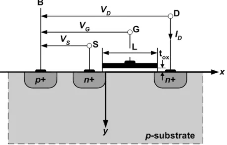
(17) Chap. 2. Subthreshold Operation of MOS Transistors. assumed to be negligible, the quasi-Fermi potential of majority carriers φ p is equal to the Fermi potential φ f and thus the channel potential is simply equal to the difference φ n - φ f. Table 2.1 Definitions used in the model. Symbols Q µn Ut=(k·T)/q ni ε s , ε ox Nsub VFB. Description Electron charge Mobility of electrons in the channel Thermal voltage Intrinsic carrier concentration Dielectric constant of Si and SiO 2 Substrate doping concentration Flat-band voltage. φ f=Ut·ln(Nsub / ni) φ s=φ(y=0). Substrate Fermi potential Surface potential. Vch=φ n - φp =φn - φ f C′ox. Channel potential Oxide capacitance per unit area. Q′inv. Mobile inversion charge per unit area. The different charges appearing across the MOS structure are represented in Fig. 2.2. The gate charge Q′G is balanced by the fixed charged Q′ox trapped at the Si- SiO 2 interface, the inversion charge Q′inv, and the depletion charge Q′B. The derivation of the characteristics of MOS transistors operating in subthreshold region begins by investigating the inversion charge in strong inversion. By integrating Poisson’s. Figure 2.2 Charges appearing across the MOS structure. 6.
(18) Chap. 2. Subthreshold Operation of MOS Transistors. equation, the mobile inversion charge density Q′inv can be expressed as a function of φ s and Vch. In the inversion region, φ s is much larger than Ut and the mobile charge density Q′inv simplifies to φ φS − 2φ f − Vch φ S Q'inv = −γ ⋅ C'ox ⋅ U t ⋅ S + exp − Ut Ut U t . (2.1). A relation between gate voltage and φ s is obtained by applying Gauss’ law: VG = V FB + φ S + γ ⋅ φS −. Q'inv C'ox. (2.2). where ? is the body effect coefficient defined as γ =. 2 ⋅ q ⋅ ε S ⋅ N sub C'ox. (2.3). In strong inversion, the surface potential φ s can be approximated by a constant φ 0 + Vch where φ 0 = 2φ f + several Ut. Replacing φ s by φ 0 + Vch in Equation 2.2 leads to an expression of the inversion charge per unit area valid in strong inversion: Q'inv = − C'ox ⋅[VG − VtB ]. (2.4). where VtB is the gate threshold voltage referred to the local substrate and defined as VtB ≡ VFB + φ0 + Vch + γ ⋅ φ 0 + Vch. (2.5). When the channel is at equilibrium (Vch = 0), the gate threshold voltage becomes VtB V. ch. =0. ≡ Vt 0 = V FB + φ0 + γ ⋅ φ0. (2.6). The inversion charge Q′inv becomes zero for a particular value of the channel potential Vp defined as the pinch-off voltage. The relation between Vp and the gate voltage is obtained from Equation 2.4 to Equation 2.6: VG V. ch. =Vp ;Q' inv =0. = VtB V. ch. =V p. [. = Vt0 + V p + γ ⋅ φ0 + V p − φ0. ]. (2.7). Each value of the gate voltage corresponds to a different value of the pinch-off voltage. By inverting Equation 2.7, the pinch-off voltage can be expressed in terms of the gate voltage:. 7.
(19) Chap. 2. Subthreshold Operation of MOS Transistors. 2 γ γ V p = VG − Vt0 − γ ⋅ VG − Vt 0 + φ0 + − φ0 + 2 2 . (2.8). The slope factor n is defined as the derivative of the gate voltage with respect to the pinch-off voltage and is given by n≡. dVG γ =1+ dV p 2 ⋅ φ0 + V p. (2.9). Since Vp depends on VG, the slope factor can also be expressed directly as a function of VG : 1 dVp = =1− n dVG. γ γ 2 ⋅ VG − Vt 0 + φ0 + 2 . 2. (2.10). This expression is useful for evaluating n at a certain operating point. For the values of ? and φ f used in practice, the pinch-off voltage is almost the linear function of the gate voltage and can be approximated by Vp ≈. VG − Vt 0 n. (2.11). where n is evaluated from Equation 2.10. Fig. 2.3 shows the pinch-off voltage calculated using Equation 2.8 and Equation 2.11 respectively. Process parameter values used for calculation are extracted from TSMC 0.25-µm CMOS process. From Fig. 2.3 we can observe that Equation 2.11 gives a good approximation for Vp when the gate voltage is below 1.1 V. The inversion charge Q′inv does not vanish abruptly when Vch reaches Vp , but decays smoothly as the channel leaves strong inversion. For Vch somewhat larger than Vp , the channel is in weak inversion and the inversion charge is much less than the charge in the depletion region. By neglecting the Q′inv term in Equation 2.2 and introducing the definition of Vt0 , the relation between the surface potential and the gate voltage is obtained:. (. VG = Vt 0 + (φS − φ0 ) + γ ⋅ φS − φ0. ). (2.12). The pinch-off voltage, which is originally defined in strong inversion, can also be used in weak inversion to approximate the surface potential. Comparing Equation 2.12 8.
(20) Chap. 2. Subthreshold Operation of MOS Transistors. Figure 2.3 Pinch-off voltage versus gate voltage.. to Equation 2.7 gives φ S = φ0 + V p. (2.13). The surface potential can finally be expressed as φ0 + V p for Vch > V p ( weak inversion) φS = φ0 + Vch for Vch ≤ V p ( strong inversion). (2.14). In weak inversion, the surface potential is smaller than 2φ f + Vch. The exponential term appearing in the general expression of the inversion charge given by Equation 2.1 is thus much smaller than φ s/Ut. The square root term in Equation 2.1 can then be written as φS − 2φ f − Vch φS φS + exp ≈ Ut Ut Ut . φS − 2φ f − Vch Ut ⋅ 1 + ⋅ exp Ut 2 ⋅ φS . (2.15). Thus the expression of the inversion charge is simplified to. Q'inv ≈ −C'ox ⋅. γ 2 ⋅ φS. φS − 2 φ f −V ch. ⋅ Ut ⋅ e. Ut. (2.16). Substituting φ s =φ 0 + Vp into Equation 2.16 gives V p −Vch. Q'inv ≈ − K w ⋅ C'ox ⋅U t ⋅ e. Ut. (2.17). where 9.
(21) Chap. 2. Subthreshold Operation of MOS Transistors φ0 − 2 φ f. K w = ( n −1 ) ⋅ e. Ut. (2.18). Assuming that the mobility µn is constant along the y axis, a general expression for the drain current including both the diffusion and the drift mechanisms can be expressed as I D = W ⋅ ( −Q'inv ) ⋅ µ n ⋅. dVch dx. (2.19). The drain current is then obtained by integrating Equation 2.19 from the source, where Vch = VS to the drain, where Vch = VD: I D = µn ⋅ C'ox ⋅. W ⋅ L. ∫. VD VS. − Q'inv ⋅ dVch = β ⋅ C'ox. ∫. VD VS. −Q'inv ⋅ dVch C'ox. (2.20). where it has been assumed that the mobility is also independent of x. The above equation is valid in all regions of operation since no assumption has been made on the mode of operation of the transistor. The drain current in weak inversion is simply obtained by integrating Equation 2.17:. I D = Kw ⋅ β. ⋅ Ut2. V p −V D Vp −VS Ut ⋅ e − e Ut . . (2.21). Substituting Equation 2.11 into Equation 2.21 gives V G −V t 0. I D = Kw ⋅ β. ⋅ U t2. ⋅e. n ⋅U t. V − VS − D Ut ⋅ e − e Ut . . (2.22). The slope factor n can be evaluated from the gate voltage by using Equation 2.10. Figure 2.4 plots the drain current versus the drain-source voltage for three values of VG - Vt0 , with β = 160 µA/V2 , Kw = 3, and n = 1.5. Notice that the drain current is almost constant when VDS > 4Ut, because the last term in Equation 2.22 is negligible in this case. Therefore, unlike in strong inversion, the minimum drain-source voltage required to force the transistor to operate as a current source in weak inversion is independent of the overdrive. Table 2.2 summarizes all the expressions for the drain current in weak inversion. The current in reverse saturation is not shown, but can be obtained by simply replacing VS by VD in the expression valid in the forward saturation region. 10.
(22) Chap. 2. Subthreshold Operation of MOS Transistors. Figure 2.4 Drain current versus drain-source voltage in weak inversion.. Table 2.2 Drain current in weak inversion. Mode. Conditions. Drain Current. VS > V p. Conduction. VD > V p. V G −V t 0. K w ⋅ β ⋅ U t2 ⋅ e. VS ≈ VD. Forward Saturation Blocked. VS > V p VD > V p VD − VS ≥ 4 ⋅ U t. VS >> V p V D >> V p. Kw ⋅ β. ⋅ U t2. ⋅e. n ⋅U t. V − VS − D ⋅ e U t − e U t . . V G −V t 0 − n ⋅V S n ⋅U t. 0. Equation 2.22 describes the general behavior of drain current in weak inversion. This expression, which is a good compromise between accuracy and simplicity, supports creative synthesis and is suitable for circuit design. Considerations for using subthreshold MOSFETs in circuit design will be discussed in the later sections.. 2.3 Efficient Design [16] In very low power applications, the use of MOS transistors operating in the weak inversion region is very attractive. However, it is not easy to manipulate the weakly inverted MOSFETs in today’s CMOS technology. The derivation of the model 11.
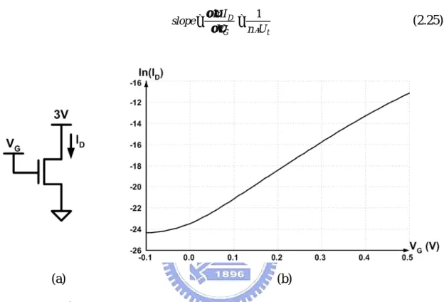
(23) Chap. 2. Subthreshold Operation of MOS Transistors. introduced in the previous section did not take higher order effects such as non-uniform doping and short-channel effects into account. On the other hand, the very accurate BSIM model is so complicated that hand calculation for an initial design is very difficult. In a design stage, we need analytical model to create a novel circuit. At the same time, we also rely on simulation results to confirm whether the circuit works. Hence, link both models together is essential in circuit design. In this section, an effective method is introduced to obtain an accurate model for initial hand calculations by extracting key parameters from simulation data. According to the analytical model introduced in the previous section, the drain current in weak inversion saturation is I D = K w ⋅ β ⋅ Ut2 ⋅ e. VG −Vt 0 n ⋅U t. ⋅e. −. VS Ut. VG. = I0 ⋅. VS. W n⋅U t − U t ⋅e ⋅e L. (2.23). where I0 =. K w ⋅ µn ⋅ C'ox ⋅U t2. ⋅e. −. Vt 0 n ⋅U t. (2.24). By examining Equation 2.23, it may be seen that that the equation is suitable for hand calculation in design stages. The parameter I0 , which is a weak function of biases and thus can be regarded as a constant, comprises all process parameters of the drain current equation. The only two process parameters in Equation 2.23 are I0 and n. The remaining terms are design parameters W/L, VG, and VS set by designers. Traditionally, parameters I0 and n are evaluated using the process parameters provided by the foundry. Although I0 and n are calculated from process parameters, the corresponding drain current ID do not match well to the ID resulting from simulation due to the inaccuracy of the simple model. Instead of evaluating the two parameters directly, we extract these values from simulation. The method to accurately obtain I0 and n will be presented later. The Berkeley Short-Channel IGFET Model (BSIM) is an accurate short-channel MOS transistor model which added numerous empirical parameters to simplify physically meaningful equations. The complete model includes very accurate expressions for DC, capacitance characteristics, and extrinsic components. For channel lengths as low as 0.25 µm, BSIM3 provides reasonable accuracy for subthreshold operation. However, BSIM3 requires approximately 180 parameters which are not directly listed in the SPICE parameter file and thus is not suitable for hand calculation.. 12.
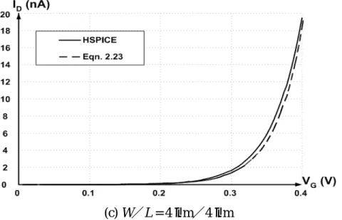
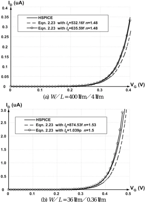
(24) Chap. 2. Subthreshold Operation of MOS Transistors. To match the analytical ID equation in Equation 2.23 to the accurate ID curves from SPICE simulation, parameter extraction for I0 and n is addressed here. Performing DC analysis on SPICE for the circuit in Fig. 2.5(a) with a given value of W/L, we obtain the ln(ID)-VG characteristic as plotted in Fig 2.5(b). From Fig. 2.5(b) we can measure the slope of the ln(ID)-VG curve. The slope can be also determined from Equation 2.23 by differentiating the drain current: slope =. ∂ ln I D 1 = ∂VG n ⋅U t. (a). (2.25). (b). Figure 2.5 (a) Tested circuit. (b) The ln(ID)-VG characteristic.. From the measured slope, the slope factor n can be calculated using Equation 2.25 and should have a value between 1.3 and 2. With W/L, VG, VS , ID, and n, the parameter I0 can be evaluated as follows: VG. VS. − I n ⋅U t U I0 = D ⋅ e ⋅e t W L. (2.26). The value of I0 is obtained by averaging the values of all I0 obtained from every simulated drain current in weak inversion. Finally, with the extracted parameters I0 and n, the ID equation in Equation 2.23 can be used as the accurate and simplified model for the weakly inverted MOSFETs. Experiments have been done by making the comparisons of ID plots from the simplified equation and those from HSPICE with three different gate width to length. 13.
(25) Chap. 2. Subthreshold Operation of MOS Transistors. ratios of 400 µm/4 µm, 40 µm/4 µm, and 4 µm/4 µm in a 0.25-µm CMOS process. I0 and n were extracted from the ln(ID)-VG curve, where W/L was set to 400 µm/4 µm. Then we used the same I0 and n but changed W/L to 40 µm/4 µm and 4 µm/4 µm to make additional comparisons. Fig. 2.6 shows the results of the comparisons of ID from the equation and HSPICE with I0 = 532.16f and n = 1.48. From Fig. 2.6(a) and (b), it is seen that the ID plots from the equation match well to those from HSPICE. The upper-end curves start splitting from each other since the MOSFET is changing from weak inversion to strong inversion. In Fig. 2.6(c), the ID curves from the equation and HSPICE do not match well because the I0 and n were extracted when W/L was 400 µm/4 µm but in (c) they were used again with W/L = 4 µm/4 µm. The gate width to length ratio has changed by a factor of 100. There is no problem between the plots in (a) and (b) even though the W/L ratio has changed by a factor of 10. Therefore, the changes of the W/L ratio should be less than a factor of 100 when we use the simplified equation.. (a) W/L = 400 µm/4 µm. (b) W/L = 40 µm/4 µm 14.
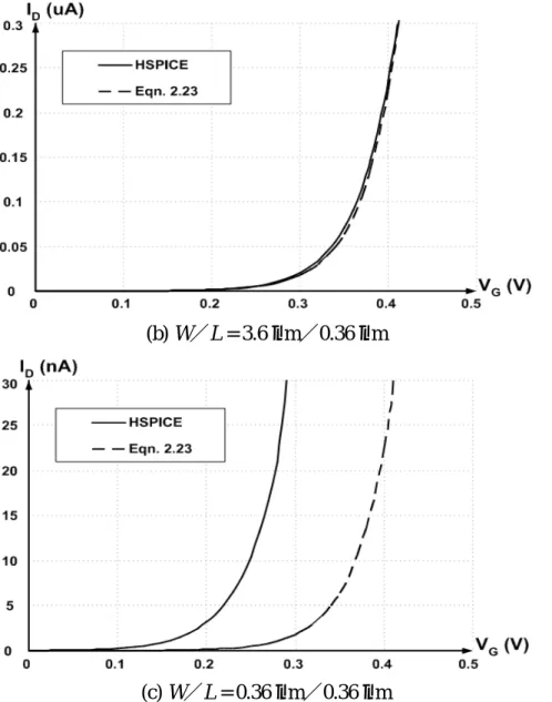
(26) Chap. 2. Subthreshold Operation of MOS Transistors. (c) W/L = 4 µm/4 µm Figure 2.6 Drain current versus gate voltage with different W/L ratios for L = 4 µm.. The same comparisons have also been done for short-channel devices with W/L ratios of 36 µm/0.36 µm, 3.6 µm/0.36 µm, and 0.36 µm/0.36 µm. With I0 = 874.53f and n = 1.53, extracted from the 36 µm/0.36 µm transistor, the ID curves are plotted in Fig. 2.7. From Fig. 2.7 we can observe that the simplified model fails to describe the drain current in weak inversion for short-channel devices if the change of the W/L ratio is larger than a factor of 10. To further investigate the simple model, the drain current plots for different bias conditions have been compared. Fig. 2.8 shows the simulated and calculated ID curves. (a) W/L = 36 µm/0.36 µm 15.
(27) Chap. 2. Subthreshold Operation of MOS Transistors. (b) W/L = 3.6 µm/0.36 µm. (c) W/L = 0.36 µm/0.36 µm Figure 2.7 Drain current versus gate voltage with different W/L ratios for L = 0.36 µm. versus gate voltage at VS = 50 mV for two different W/L ratios of 400 µm/4 µm and 36 µm/0.36 µm. In Fig. 2.8, deviations are observed between the ID curve calculated using previously extracted parameters and the simulated ID curve. By re-extracting I0 and n at VS = 50 mV, the curves from the equation and simulation become matched. The technique described in this section maps the BSIM model to an analytical model. This gets accuracy from the accurate model and puts it into a simpler model. The experimental results have confirmed that the technique is useful for low-power low-voltage designs using subthreshold MOSFETs.. 16.
(28) Chap. 2. Subthreshold Operation of MOS Transistors. (a) W/L = 400 µm/4 µm. (b) W/L = 36 µm/0.36 µm Figure 2.8 Drain current versus gate voltage at VS = 50 mV with different W/L ratios.. 2.4 Mismatch Mismatch is the differential performance of two or more devices on a single integrated circuit (IC). It is widely recognized that mismatch is key to precision analog IC design. As stated above, subthreshold operation is attractive for low-power design. The exponential dependence of drain current on gate-to-source voltage provides a very useful property for many applications. However, one of the major disadvantages associated with weakly inverted MOSFETs is the current mismatch between identical drawn devices. Owing to exponential dependencies on the process 17.
(29) Chap. 2. Subthreshold Operation of MOS Transistors. variations, devices in subthreshold usually exhibit larger mismatch in drain current as compared with that in above-threshold [14]. The effect of MOS transistor mismatch is therefore prominent for using subthreshold MOSFETs in circuit design. In the following paragraphs, the mismatch models for MOS transistors and matching properties in the weak inversion region are discussed. MOSFET current mirrors and differential pairs, which are widely used in analog integrated circuits, are usually investigated for transistor mismatch characterization [17]-[24]. Assuming that the drain current is a function of the overdrive VG - Vt0 rather than a function of VG and Vt0 separately, the mismatch of drain currents in two identical transistors which have the same gate voltage can be modeled as ∆I D ∆β gm = − ⋅ ∆ Vt 0 ID β ID. (2.27). where ∆Vt0 and ∆β/β are the threshold voltage mismatch and the current factor mismatch respectively. The current mismatch is maximum in weak inversion, for which gm /ID is maximum, and only comes down to ∆β/β when the transistors operate deeply in strong inversion. The threshold voltage mismatch ∆Vt0 and the current factor mismatch ∆β/β are usually used as the two parameters to characterize the matching properties of MOS transistors. Pelgrom et al. [17] introduced a powerful spatial Fourier transform technique to build a general frame for mismatch parameters. Neglecting the separation-dependant mismatch effects, the standard deviations of the threshold voltage mismatch and the current factor mismatch are inversely proportional to the square root of the transistor area: σ (∆Vt 0 ) =. AVt 0 W ⋅L Aβ. σ (∆β ) = β W ⋅L. (2.28). where AVt0 and Aβ are the size proportionality constants for s (∆Vt0 ) and s(∆β)/β respectively. Experimental results showed that Equation 2.28 could predict the threshold voltage mismatch and the current factor mismatch. The two proportionality constants, AVt0 and Aβ , could be derived from the measured mismatch in threshold voltage and current factor. It was also observed that the threshold voltage mismatch decreased with thinner gate oxides, whereas the current factor mismatch remained almost constant.. 18.
(30) Chap. 2. Subthreshold Operation of MOS Transistors. With respect to the mismatch in subthreshold MOSFETs, Forti and Wright [18] measured the current mismatch in MOS differential pairs operated in the weak inversion region. They measured a total of about 1400 NMOS and PMOS transistors produced in four different processes with different oxide thickness and feature sizes. Using the scaled current I = ID/(W/L), a fairly good uniformly response was found over a wide variety of sizes and VGS values. The measured weak inversion current mismatch was essentially independent of current density as expected and it was observed to be proportional to the inverse square root of device area except for the big transistors and for the PMOS transistors. Furthermore, the substrate bias was judged to be responsible for significant degradation in match. Chen et al. [19], [20] measured and analyzed the current mismatch of weakly inverted MOS transistors with substrate-to-source junction forward and reverse biased. The MOS transistor with substrate-to-source junction slightly forward biased acts as a high gain gated lateral bipolar transistor in low level injection. The measured mismatch data exhibited that i) subthreshold circuits should be carefully designed for suppression of mismatch arising from back- gate reverse bias, and ii) the current match in weak inversion can be substantially improved by the gated lateral action, especially for small size transistors. An analytical statistical model with back- gate forward bias and device size both as input parameters for optimizing the match can be found in [20]. The mismatch model of MOS transistors derived in [17] has been found in good agreement with experimental results for a device size above 2 µm. However, it was observed that the threshold voltage mismatch linear dependence on the inverse of the square root of the device area no longer holds for transistors with L = 0.7 µm [21]. Due to the strong dependence of the threshold voltage and of the effective mobility on channel length for short-channel transistors, the mismatch model described in Equation 2.28 is not applicable for submicron devices. The mismatch model proposed by Croon et al. [22], [23] is based on parametric extensions of [17] and is validated on a 0.18-µm technology. The mismatch model contains four parameters: one parameter (∆Vt0 ) to describe the mismatch in the threshold voltage, and three (∆β 0 , ∆ζsr, and ∆ζsat) to describe the mismatch in the current factor. The parameter ∆β 0 is the low field current factor for long transistors while the other two parameters, ∆ζsr and ∆ζsat, are used to model the higher order effects such as surface roughness scattering, series resistance, and velocity saturation. These mismatch parameters are modeled by the complete Pelgrom model [17]:. 19.
(31) Chap. 2 σ 2 (∆ P ) =. Subthreshold Operation of MOS Transistors. AP2,0 A2 A2 + P , L2 + P2 ,W W ⋅L W ⋅L W ⋅L. (2.29). The first term of the right-hand side models the variance for a large device, while the second and third terms describe the variation in short and narrow channel effects. The correlation factors between mismatch parameters can also be modeled by ρ P1 , P2 = AP1 2 ,0 +. AP1 2 , L L. +. AP1 2 ,W W. (2.30). The first term on the right-hand side gives the correlation for large transistors, while the second and third terms account for short and narrow channel effects. The detailed mismatch model in drain current and the procedure for extracting the mismatch parameters can be found in [23].. 20.
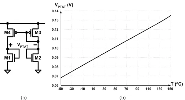
(32) CHAPTER. 3 CMOS PTAT REFERENCES This chapter deals with the analysis and design of MOS PTAT references. We describe the operation principles of MOS PTAT prototypes and analyze these circuits in detail. In addition to this, low- voltage PTAT generators which are applicable in deep-submicron technology have been also investigated. In the end of this chapter, the effects of leakage current at high temperature are discussed and a compensation technique to enhance the linearity is proposed.. 3.1 Introduction The PTAT circuits generate an output voltage proportional to absolute temperature and have been widely used in temperature- insensitive voltage and current references. In a thermal management system, the PTAT reference is also the best candidate for a fully- integrated temperature sensor. Traditionally, PTAT references are implemented using parasitic substrate bipolar transistors available in all standard CMOS processes. A typical PTAT generator using parasitic BJTs is shown in Fig. 3.1. When both transistors are at the same temperature, the difference between emitter-to-base voltages, ∆VEB, of two diode- like bipolar transistors can be written as I I ∆ VEB = V EB1 − V EB2 = U t ⋅ ln 1 S 2 I 2 I S1. . (3.1). where Ut is the thermal voltage and IS1 as well as IS2 are the saturation current for Q1 and Q2 respectively. If the two transistors are matched, ∆VEB is directly proportional to absolute temperature, i.e., it is a PTAT signal. Various on-chip PTAT references have been extensively implemented using 21.
(33) Chap. 3 CMOS PTAT References. Figure 3.1 Typical PTAT generator.. parasitic BJTs because of the ease of design. In some CMOS process, however, obtaining reliable BJTs is very costly and the desirable performance from these parasitic devices is hard to expect. Also, the power consumption of the BJT based references is relatively high and an alternative approach is preferred, especially in low power applications. Several PTAT references using the subthreshold MOS transistors have been studied and applied in low-power low-voltage designs [12], [13], [25]-[30]. These circuits take advantage of MOS devices operating in the weak inversion region in two respects: i) the exponential I-V characteristic is used to generate a PTAT voltage, and ii) the power consumption is made minimum due to the inherent low currents in that region. The properties of MOS PTAT references make them an excellent temperature sensor in a thermal management system. To implement the competitive temperature sensors in deep-submicron technology, we first analyze the prototype circuits of MOS PTAT references in the following section.. 3.2 MOS PTAT Generator Prototypes Several kinds of MOS PTAT generators have been reported for use in a wide range of applications. All of these PTAT circuits can be categorized into three types. In this section, the prototype circuits of MOS PTAT generators will be introduced and analyzed. 3.2.1. Prototype I: Diode Connection. The first MOS PTAT prototype [25] is shown in Fig. 3.2. If transistors M1 and M2 operate in weak inversion, the drain currents of M1 and M2 are given by. 22.
(34) Chap. 3 CMOS PTAT References. Figure 3.2 MOS PTAT generator prototype I: diode connection.. V1 −V t 0 ,1 − (n1 −1 )⋅V S. I D1 =. K w1 ⋅ β1 ⋅ Ut2. ⋅e. I D2 = K w 2 ⋅ β 2 ⋅ U t2 ⋅ e. n1 ⋅U t V 2 −Vt 0 , 2 −( n 2 −1 )⋅V S. (3.2). n 2 ⋅Ut. where it is assumed that V1,2 >> Ut. Equation 3.2 can be derived to I V1 = Vt 0,1 + (n1 − 1) ⋅ VS + n1 ⋅ Ut ⋅ ln D1 A1 I V2 = Vt0 ,2 + (n2 − 1) ⋅ VS + n2 ⋅ Ut ⋅ ln D 2 A2 . (3.3). A1,2 = K w1,2 ⋅ β1,2 ⋅ U t2. (3.4). where. If M1 and M2 are matched, the PTAT voltage can be obtained from the difference in V1 and V2 : I S VPTAT = V1 − V2 = n ⋅ U t ⋅ ln D1 ⋅ 2 I D2 S1 . (3.5). where S1 and S2 are the W/L ratios of M1 and M2 respectively. To examine the temperature characteristic of the prototype, we have simulated the circuit shown in Fig. 3.3(a) in a 0.25-µm CMOS process. In this circuit, p-channel MOSFETs M3 and M4 act as a current mirror and the minimum supply voltage for which M3 and M4 operate in the strong inversion saturation region is VDD ,min = VGS ,w + VSG, p. (3.6). where VGS,w represents the gate-source voltage of the transistor in weak inversion and VSG,p is the source-gate voltage of PMOS transistors. In the simulation, the device sizes S1 and S2 are set to equal while the current ratio ID1 /ID2 is 10. The PTAT voltage 23.
(35) Chap. 3 CMOS PTAT References. (a). (b). Figure 3.3 Simulation of MOS PTAT prototype I. (a) Simulation circuit. (b) PTAT voltage versus temperature.. versus temperature plot is shown in Fig. 3.3(b). Equation 3.5 is based on the assumption that transistors M1 and M2 are perfectly matched. In reality, however, nominally identical devices suffer from a finite mismatch due to uncertainties in each step of the manufacturing process. To take into account the threshold voltage and the current factor mismatch in the circuit shown in Fig. 3.3(a), we now define average and mismatch quantities as follows:. Vt 0 =. Vt 0,1 + Vt 0,2. 2 ∆ Vt 0 = Vt 0,1 − Vt 0,2. (3.7). β1 = S1 ⋅ β w1 β 2 = S 2 ⋅ β w2 β w1 + β w 2 2 ∆ β w = β w1 − β w 2 βw =. (3.8). β 3 = S3 ⋅ β p3 β 4 = S4 ⋅ β p4 βp =. β p3 + β p4. (3.9). 2 ∆ β p = β p3 − β p4. 24.
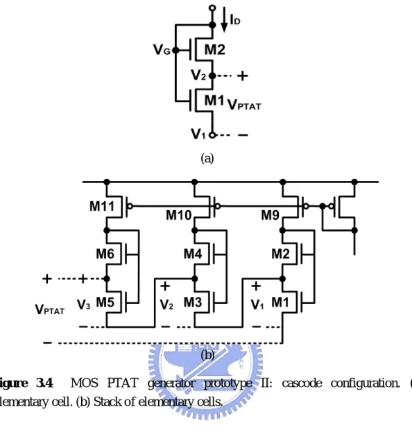
(36) Chap. 3 CMOS PTAT References. These relations can be inverted to give the original parameters in terms of the average and the mismatch parameters. For example, ∆β w β1 = S1 ⋅ β w + 2 ∆βw β2 = S 2 ⋅ βw − 2 . (3.10). Applying this set of equations for the various parameters in Equation 3.3 and solving for V1 - V2 , we obtain S S 1 − ∆β p 2 ⋅ β p V1 − V2 = ∆Vt 0 + n ⋅ U t ⋅ ln 4 ⋅ 2 + ln 1 + ∆β p 2 ⋅ β p S3 S1 . + ln 1 − ∆β w 2 ⋅ β w 1 + ∆β 2 ⋅ β w w . (3.11). If ∆β p,w/2·βp,w << 1, the last two terms in the above equation can be written as 2. 1 − ∆β p, w 2 ⋅ β p, w ∆ β p, w ∆ β p, w ≈ ln1 − ≈− ln 1 + ∆β 2⋅β 2 ⋅ β β p ,w p, w p, w p, w . (3.12). Substituting these approximations into Equation 3.11 gives ∆β p ∆β w + ∆Vt0 ⋅ + βp β w ∆β p ∆β w = VPTAT ,ideal − n ⋅ Ut ⋅ + + ∆ Vt 0 βp β w . S S V1 − V2 ≈ n ⋅ Ut ⋅ ln 4 ⋅ 2 − n ⋅ U t S3 S1 . (3.13). Equation 3.13 indicates that the accuracy of the PTAT signal is strongly dependent on the mismatch in transistors since the value of VPTAT is usually smaller than 100 mV at room temperature. 3.2.2. Prototype II: Cascode Configuration. The second MOS PTAT prototype [26], [27] is shown in Fig. 3.4. In the elementary cell, the two transistors M1 and M2 both operate in the subthreshold region. Because M2 is diode connected, it operates in the forward saturation mode and forces M1 to operate in the conduc tion mode. Since M2 operates in the saturation mode, V G −V t 0 ,2 − n 2 ⋅V 2. ID =. K w 2 ⋅ β 2 ⋅ U t2. ⋅e. n 2 ⋅U t. (3.14). Since M1 operates in the conduction mode,. 25.
(37) Chap. 3 CMOS PTAT References. (a). (b) Figure 3.4 MOS PTAT generator prototype II: cascode configuration. (a) Elementary cell. (b) Stack of elementary cells.. V G −V t 0 ,1. ID =. K w1 ⋅ β1 ⋅ U t2. ⋅e. n1 ⋅U t. V − V1 − 2 Ut ⋅ e − e Ut . . (3.15). If M1 and M2 are matched, the PTAT voltage can be derived from Equation 3.14 and Equation 3.15: S V PTAT = V2 − V1 = U t ⋅ ln1 + 2 S1 . (3.16). where S1 and S2 are the W/L ratios of M1 and M2 respectively. Values of VPTAT practically obtainable from an elementary cell are limited to about 100 mV. Higher values may be obtained by stacking a certain number of cells as shown in Fig. 3.4(b). In this circuit, the voltage VPTAT is composed of three sections. The mode of operation is still the same, except that the current supplied to each cell goes through the bottom transistor of all subsequent cells. For instance, the PTAT voltage formed by section 26.
(38) Chap. 3 CMOS PTAT References. M1-M2 is given by S S + S10 + S11 V1 = U t ⋅ ln1 + 2 ⋅ 9 S1 S9 . (3.17). where S9 , S10 , and S11 are W/L ratios of the respective MOSFETs. Fig. 3.5 shows the simulated circuit and the PTAT voltage plot of this prototype. In Fig. 3.5(a), the transistor M3 which operate in strong inversion serves as a current source and the minimum supply voltage is given by VDD ,min = VGS ,w + VSG, p. (3.18). Fig. 3.5(b) shows the simulated VPTAT with S2 /S1 = 9. The curve deviates from the straight line at high temperature due to the effect of leakage currents.. (a). (b). Figure 3.5 Simulation of MOS PTAT prototype II. (a) Simulation circuit. (b) PTAT voltage versus temperature.. We now consider the effect of transistor mismatch in the circuit shown in Fig. 3.5(a). Applying the expressions in Equation 3.7 and Equation 3.8 and neglecting high-order terms, we obtain. VPTAT. ∆Vt 0 ∆β w n⋅U t S2 ⋅e ≈ U t ⋅ ln 1 + ⋅ 1 − S1 β w . (3.19). 27.
(39) Chap. 3 CMOS PTAT References. If S2 >> S1 , the PTAT voltage can be rewritten as S ∆β ∆Vt 0 VPTAT ≈ U t ⋅ ln 2 − U t ⋅ w + S β n 1 w ∆β ∆Vt 0 = VPTAT ,ideal − U t ⋅ w + βw n. (3.20). In Fig. 3.4(b), the PTAT voltages V1 , V2 , and V3 can also be derived similarly and have the same mismatch terms as in Equation 3.20 except the presence of ∆β p /βp due to the current mismatch in the PMOS current mirror. Since the voltage variations of the three cells are not statistically correlated, the standard deviation of the voltage variation is therefore multiplied by 3 and the spread of VPTAT is reduced. 3.2.3. Prototype III: Common Gate Connection. Fig. 3.6 shows the third MOS PTAT prototype [12], [13], [27]-[30]. If transistors M1 and M2 are in weak inversion and their drain-source voltages are both much larger then Ut, the drain currents can be expressed as V G −V t 0 ,1 − n 1 ⋅V1. I D1 =. K w1 ⋅ β 1 ⋅ U t2. ⋅e. n1 ⋅U t V G −Vt 0 , 2 − n 2 ⋅V 2. I D2 = K w2 ⋅ β 2 ⋅ U t2 ⋅ e. (3.21). n 2 ⋅U t. Assuming that M1 and M2 are matched, the PTAT signal can be obtained and is given by I S V PTAT = V1 − V2 = U t ⋅ ln D 2 ⋅ 1 I D1 S2 . (3.22). where S1 and S2 are the W/L ratios of M1 and M2 respectively.. Figure 3.6 MOS PTAT generator prototype III: common gate connection.. 28.
(40) Chap. 3 CMOS PTAT References. We also examine the temperature characteristic of this prototype circuit through simulation. The simulated circuit shown in Fig. 3.7(a) is derived from a circuit used with bipolar transistors and has been utilized in several designs. The p-channel MOSFETs M3 and M4 act as a current mirror and the minimum supply voltage is given by VDD ,min = VPTAT + V DS, w + VSG, p. (3.23). where VDS,w is the drain-source voltage of the transistor in weak inversion. In the simulation, the device size ratios S1 and S2 are set to equal while the current ratio ID2 /ID1 is 10. Fig. 3.7(b) shows the PTAT voltage VPTAT versus temperature. At high temperature, deviations from the ideal PTAT behavior due to leakage currents are also observed.. (a). (b). Figure 3.7 Simulation of MOS PTAT prototype III. (a) Simulation circuit. (b) PTAT voltage versus temperature.. Consider the circuit shown in Fig. 3.7(a). The variation of VPTAT may come from threshold voltage and current factor mismatch in M1-M2 pair and the current mismatch in the current mirror formed by M3 and M4. Applying the mismatch parameters defined by Equation 3.7 to Equation 3.9 in the derivation of VPTAT, we obtain. 29.
(41) Chap. 3 CMOS PTAT References ∆β ∆β p ∆Vt 0 − ⋅ w + βw β n p ∆β ∆β p ∆Vt 0 − + Ut ⋅ w + βw β n p . S S VPTAT ≈ Ut ⋅ ln 1 ⋅ 3 + Ut S 2 S4 = VPTAT ,ideal. (3.24). Note that the mismatch terms in Equation 3.24 are almost the same as those in Equation 3.20. In this circuit, the mismatch of resistor does not affect the PTAT voltage as long as M1 and M2 both operate in weak inversion. 3.2.4. Summary. The temperature and mismatch characteristics of MOS PTAT prototypes have been addressed in the previous paragraphs. These results are summarized in Table 3.1. The ∆βp /βp terms are omitted in expressions of ∆VPTAT since the current factor mismatch in strong inversion is negligible compared to that in weak inversion. The PTAT signal of prototype I is proportional to nUt while the other two prototype circuits generate output voltages proportional to Ut. The value of the slope factor n ranges usually from 1.3 to 2 and a larger VPTAT can be obtained in prototype I. In a standard CMOS process, however, the slope factor is not a reliable parameter and its value depends slightly on the bias conditions. Furthermore, the higher supply voltage requirement due to diode-connected transistors makes prototype I incompatible with low-voltage operation.. Table 3.1 Characteristics of MOS PTAT prototypes. Prototype. VPTAT. ∆VPTAT. I S n ⋅ U t ⋅ ln D1 ⋅ 2 I D2 S1 . ± n ⋅ Ut ⋅. S U t ⋅ ln1 + 2 S1 . ±Ut ⋅. I S U t ⋅ ln D2 ⋅ 1 I D1 S2 . ±Ut ⋅. ∆β w ± ∆Vt0 βw. VDD,min VGS ,w + VSG, p. [25]. ∆β w ∆Vt0 ± βw n. VGS ,w + VSG, p. [26] [27]. ∆β w ∆Vt0 ± βw n. VPTAT + V DS ,w + VSG , p. [27] | [30]. 30.
(42) Chap. 3 CMOS PTAT References. The characteristics of prototypes II and III are very similar. Prototype II provides a floating PTAT voltage and the elementary cells can be stacked to produce PTAT voltages of the order of a few hundreds of millivolts. As an additional advantage, the mismatch between transistors is averaged out in a stacked PTAT generator. The spread of VPTAT can be reduced at the expense of a larger supply voltage.. 3.3 Low-Voltage PTAT References in Deep-Submicron Technology Low- voltage implementations for PTAT references are necessary for the complete system-on-chip such as thermal management system. Such PTAT references must exhibit the best compatibility in deep-submicron technology. In the following paragraphs, we will investigate the low-voltage MOS PTAT references in detail. 3.3.1. Power-Supply Rejection Ratio (PSRR). The MOS PTAT prototype circuit shown in Fig. 3.7(a) seems suitable for low-voltage designs. However, the power-supply rejection ratio (PSRR) of this circuit deteriorates sharply in deep-submicron technology. Fig. 3.8 shows the low- frequency small-signal model of the MOS PTAT generator shown in Fig. 3.7(a). From Fig. 3.8, the small-signal gain v ptat/vdd can be derived to v ptat vdd. =. (. R ⋅ g4 ⋅ g '2 ⋅ go1 + g m1 ⋅ g o3. ). g'2 ⋅ ( go1 + g 4 + g1 ⋅ g 4 ⋅ R) − g m1 ⋅ g m3. (3.25). where g′2 = g2 + go3 . In most practical cases, gm1 >> go1 , gm2 >> go2 + go3 , and gm4 >> go4 + go1 . Then. Figure 3.8 Low- frequency small-signal model of the MOS PTAT generator shown in Fig. 3.7(a). 31.
(43) Chap. 3 CMOS PTAT References v ptat vdd. ≈. R ⋅ g m4 ⋅ ( g m2 ⋅ g o1 + gm1 ⋅ go3 ). gm2 ⋅ gm4 ⋅ (1 + g m1 ⋅ R ) − gm1 ⋅ gm3. (3.26). Since M1 and M2 are in weak inversion and M3 and M4 act as a current mirror, g m2 I D2 S 3 g m3 = = = ≡P g m1 I D1 S 4 gm 4. (3.27). Substituting Equation 3.27 into Equation 3.26, we have v ptat vdd. ≈. go1 + go3 P gm1. (3.28). In deep-submicron technology, the ratio gm1 /go1 is typically smaller than 200 and the resulting static PSRR+ is usually smaller than 50 dB. Fig 3.9 shows the simulated VPTAT and static PSRR+ versus supply voltage at room temperature for the PTAT generator shown in Fig. 3.7(a). For PSRR(DC)+ > 40 dB, the minimum supply voltage is 1.5 V.. Figure 3.9 Simulated VPTAT and static PSRR+ versus supply voltage at room temperature for the PTAT generator shown in Fig. 3.7(a).. A low-voltage MOS PTAT reference based on the same prototype [13] is depicted in Fig. 3.10. The simple current mirror in Fig. 3.7(a) is replaced by the operational transresistance amplifier (ORA) composed of M3-M8. The role of the ORA is to ensure the current ratio ID2 /ID1 , as well as an almost equal voltage biasing for both drain voltages of M1 and M2. Thanks to the latter, the channel length modulation effects in M1-M2 can be minimized. 32.
(44) Chap. 3 CMOS PTAT References. Figure 3.10 The low-voltage MOS PTAT reference.. The small-signal DC gain v ptat/v dd of this circuit can be derived from the low- frequency small-signal model shown in Fig. 3.11. Assume go << gm for all transistors, then v ptat vdd. ≈. R ⋅ gm 4 ⋅ gm6 ⋅ gm8 ⋅ ( gm 2 ⋅ go1 − gm1 ⋅ go 2 ). gm2 ⋅ gm4 ⋅ g m6 ⋅ g m8 ⋅ (1 + g m1 ⋅ R ) − gm1 ⋅ gm3 ⋅ g m5 ⋅ gm7. (3.29). If gm3 = gm4 and gm6 = gm7 , the above equation can be rewritten as v ptat vdd. ≈. R ⋅ g m8 ⋅ ( gm 2 ⋅ go1 − gm1 ⋅ go 2 ). gm 2 ⋅ gm8 ⋅ (1 + gm1 ⋅ R ) − g m1 ⋅ gm5. (3.30). Figure 3.11 Low- frequency small- signal model of the MOS PTAT reference shown in Fig. 3.10.. Ideally, gm1,2 and go1,2 are all proportional to their drain currents since M1 and M2 are both in weak inversion. As a result, gm2 ·go1 = gm1 ·go2 and PSRR+ approximates to infinity for low frequencies. The finite static PSRR+ may arise from the higher order 33.
(45) Chap. 3 CMOS PTAT References. effects in gm and go in reality. Fig. 3.12 shows the simulated VPTAT and PSRR(DC)+ versus supply voltage at room temperature for the low-voltage PTAT reference. From Fig. 3.12 we can observe that the static PSRR+ is improved significantly. For PSRR(DC)+ > 40 dB, the minimum supply voltage is 1.1 V and the PSRR+ is greater than 70 dB for VDD = 1.5 V.. Figure 3.12 Simulated VPTAT and static PSRR+ versus supply voltage at room temperature for the low-voltage PTAT reference shown in Fig. 3.10.. 3.3.2. Accuracy. The use of ORA in the low-voltage PTAT reference may lead to a larger spread of VPTAT due to the extra current mirrors. Defining average and mismatch quantities, we have Vt 0 =. Vt 0,1 + Vt 0,2. 2 ∆ Vt 0 = Vt 0,1 − Vt 0,2. (3.31). β1 = S1 ⋅ β w1 β 2 = S 2 ⋅ β w2 β w1 + β w 2 2 ∆ β w = β w1 − β w 2 βw =. (3.32). β 3 = S3 ⋅ β n3 β 4 = S4 ⋅ β n 4 β n3 + β n4 2 ∆ β n = β n3 − β n 4 βn =. (3.33). 34.
(46) Chap. 3 CMOS PTAT References β 5−8 = S5 −8 ⋅ β p5− 8 β p5− 8 = β p ±. (3.34). ∆β p 2. Applying this set of equations in the derivation of VPTAT, we obtain S S S S ∆β n 2 ⋅ ∆ β p ∆β w ∆Vt0 VPTAT ≈ Ut ⋅ ln 1 ⋅ 3 ⋅ 7 ⋅ 5 + + + − βp β w n S2 S4 S 6 S8 β n = VPTAT ,ideal. ∆β 2 ⋅ ∆β p ∆β w ∆ Vt 0 − + Ut ⋅ n + + βn βp β w n . (3.35). In this circuit, the VPTAT variation due to current factor mismatch in strong inversion is approximately three times as large as that in conventional MOS PTAT circuits. 3.3.3. Circuit Compensation. The low-voltage MOS PTAT reference has two feedback paths and may require proper compensation. Consider the open- loop circuit shown in Fig. 3.13. The first feedback path consists of a common-source stage with source degeneration and a current mirror. Therefore, the small-signal current i′1 can be expressed as i1' =. gm1 ⋅ ro1 ⋅ vi. ⋅. S7. ro1 + [1 + (g m1 + gmb1 ) ⋅ ro1 ] ⋅ R S8. (3.36). The second path consists of a common-source stage and two current mirrors and the small-signal current i′2 is given by i2 = g m2 ⋅ vi ⋅ '. S6 S 4 ⋅ S5 S3. (3.37). Figure 3.13 Open- loop circuit of the low- voltage MOS PTAT reference.. 35.
(47) Chap. 3 CMOS PTAT References. The small-signal gain v o /v i is thus A0 =. vo i' − i' = − 2 1 ⋅ (ro4 || ro7 ) vi vi. (3.38). If S3 = S4 , S6 = S7 , and S5 = P·S8 , then A0 becomes A0 = − g m1 ⋅. S6 ro1 ⋅ (ro4 || ro7 ) ⋅ 1 − S8 ro1 + [1 + (g m1 + gmb1 ) ⋅ ro1 ] ⋅ R . (3.39). In general, (gm1 + gmb1 )·ro1 >> 1 and the above equation can be rewritten as A0 = − g m1 ⋅. S6. ⋅. S8. (g m1 + gmb1 ) ⋅ R ⋅ ( ro4 || ro7 ) 1 + ( gm1 + g mb1 ) ⋅ R. (3.40). The dominant pole is located at the output node and is given by p1 =. 1. (ro 4 || ro7 ) ⋅ C. (3.41). Therefore, the gain-bandwidth product can be expressed as ωGB =. gm1 C. ⋅. ( g m1 + gmb1 ) ⋅ R S6 ⋅ 1 + (g m1 + g mb1) ⋅ R S8. (3.42). Values of gm1 and C must be designed so that the gain-bandwidth product is well below the other poles arising from parasitic capacitances. Fig. 3.14 shows the simulated frequency response of the open- loop circuit for three values of gm1 /C. The unit-gain frequency is found proportional to gm1 /C as described in Equation 3.42.. Figure 3.14 Frequency response of the open-loop circuit shown in Fig. 3.13. 36.
(48) Chap. 3 CMOS PTAT References. 3.3.4. All-MOS Implementations. The presence of the resistor may be a drawback in a low-voltage MOS PTAT reference. For an extremely low bias current, a high value resistance is required which takes a large surface area. The resistivity is also not guaranteed by some foundries and may vary with technology. The resistor of the PTAT generator in Fig. 3.10 can be replaced by a MOSFET working below saturation [13], [29]. Fig. 3.15 depicts the all-MOS implementations for the low-voltage PTAT reference. In both circuits, transistor M9 operates in the strong inversion conduction mode while M10 and M11 are in the strong inversion saturation mode.. (a). (b) Figure 3.15 Low- voltage MOS PTAT references with all-MOS implementation. 37.
(49) Chap. 3 CMOS PTAT References. The drain currents of M9 and M10 are given by [15] n I D9 = β 9 ⋅ VG − Vt 0 − ⋅ VPTAT 2 1 2 I D10 = β 10 ⋅ (VG − Vt 0 ) 2 ⋅n. ⋅ VPTAT . (3.43). For the circuit in Fig. 3.15(a), I D9 I S = D8 = 8 I D10 I D11 S11. (3.44). Substituting Equation 3.43 into Equation 3.44 and solving for VG- Vt0 , we obtain. (. VG − Vt 0 = n ⋅ VPTAT ⋅ K + K ⋅ ( K − 1). ). (3.45). where K=. S9 S11 ⋅ S10 S8. (3.46). Therefore, the drain current of M9 in Fig. 3.15(a) is 1 2 I D9 = I D1 = β 9 ⋅ n ⋅ V PTAT ⋅ K − + K ⋅ (K − 1) 2 . (3.47). For given values of VPTAT and ID1 , the transistor size S9 can be evaluated from Equation 3.47. Similarly, the drain current of M9 in Fig. 3.15(b) can also be obtained in the same way. Assume that S10 = N·S9 and S11 = M·S8 , then I D9 1 =1+ I D10 M. (3.48). The drain current of M9 in Fig. 3.15(b) can therefore be derived to M N 1 2 I D9 = (1 + M ) ⋅ I D1 = β 9 ⋅ n ⋅ VPTAT ⋅ ⋅ 1 + 1 + N + + N ⋅ (1 + M ) M 2 . (3.49). Also, for given values of the PTAT voltage and the bias current, the transistor size S9 can be determined.. 38.
(50) Chap. 3 CMOS PTAT References. 3.4 Leakage Currents and Proposed Compensation Technique There are at least three essential requirements for the PTAT reference in an on-chip temperature sensor: i) the circuit must exhibit the best compatibility against process scaling, ii) the supply voltage should be compatible with the complete system-on-chip, and iii) the PTAT signal must be linear over a wide range of temperature. The low-voltage PTAT generators described in the previous section fulfill the first two requirements for a complete temperature sensor. However, these circuits suffer from the nonlinearity problem if the temperature is higher than 100°C. This nonlinear behavior mainly results from the junction leakage currents in MOS transistors at high temperature. In this section, we first discuss the effect of leakage currents and then a compensation technique is proposed to enhance the linearity of high temperature behavior. In the CMOS structure, the source/drain implants and the substrate (or the n-well) form the pn junction diodes and may conduct leakage currents in the devices. Fig. 3.16 illustrates the leakage currents through the junction diodes in MOS transistors. These leaky diodes are generally reverse-biased since the bulk of n-channel MOSFETs is tied to the ground and that of p-channel MOSFETs to the most positive supply voltage. The leakage current which is the reverse-bias saturation current of the diode is associated with the doing concentrations and is strongly dependent on temperature.. Figure 3.16 The leaky junction diodes in MOS transistors.. At room temperature, these leaky diodes conduct almost no current and do not influence the operation of transistors. However, the leakage current increases sharply in high temperature and degrades the performance of analog circuits. Fig. 3.17 shows the leakage current versus temperature in a 0.25-µm CMOS process. Leakage currents. 39.
(51) Chap. 3 CMOS PTAT References. in both n-channel and p-channel MOSFETs with different channel widths and lengths are plotted in this figure. The leakage current is found slightly dependent on the channel length and proportional to the gate wid th since the current in a diode is proportional to its area. Furthermore, n-channel MOSFETs have larger leakage current s due to the lower channel doping concentration.. Figure 3.17 Leakage current versus temperature.. Due to the extremely low current in weak inversion, the leakage current becomes comparable to the current level in a MOS PTAT generator. Fig. 3.18 shows the VPTAT curves of the circuit in Fig. 3.15(a) with different values of ID1 . For smaller bias current level, the influence of leakage cur rents on the PTAT voltage is more severe.. Figure 3.18 VPTAT curves of the circuit in Fig. 3.15(a) with different ID1 .. 40.
數據
+7

相關文件
6 《中論·觀因緣品》,《佛藏要籍選刊》第 9 冊,上海古籍出版社 1994 年版,第 1
Reading Task 6: Genre Structure and Language Features. • Now let’s look at how language features (e.g. sentence patterns) are connected to the structure
Robinson Crusoe is an Englishman from the 1) t_______ of York in the seventeenth century, the youngest son of a merchant of German origin. This trip is financially successful,
fostering independent application of reading strategies Strategy 7: Provide opportunities for students to track, reflect on, and share their learning progress (destination). •
This Manual would form an integral part of the ‘School-based Gifted Education Guideline’ (which is an updated version of the Guidelines issued in 2003 and is under preparation)
• Thresholded image gradients are sampled over 16x16 array of locations in scale space. • Create array of
溫度轉換 自行設計 溫度轉換 自行設計 統計程式 簡單 簡單 統計程式.
This design the quadrature voltage-controlled oscillator and measure center frequency, output power, phase noise and output waveform, these four parameters. In four parameters
