國 立 交 通 大 學
電子工程學系 電子研究所碩士班
碩 士 論 文
具奈米線通道的薄膜電晶體之氮化矽記憶體元件
特性分析
Characterizations of TFT-SONOS with Nanowire
Structure
研 究 生:黃建富
指導教授:黃調元 博士
林鴻志 博士
具奈米線通道的薄膜電晶體之氮化矽記憶體元件
特性分析
Characterizations of TFT-SONOS with Nanowire
Structure
研 究 生
:黃建富 Student:Jian-Fu Huang
指導教授 :黃調元 博士 Advisors:Dr. Tiao-Yuan Huang
林鴻志 博士
Dr. Horng-Chih Lin
國 立 交 通 大 學
電子工程學系 電子研究所碩士班
碩 士 論 文
A Thesis
Submitted to Department of Electronics Engineering & Institute of Electronics College of Electrical Engineering and Computer Science
National Chiao-Tung University in Partial Fulfillment of the Requirements
for the Degree of Master of Science
in
Electronic Engineering June 2007
Hsinchu, Taiwan, Republic of China
具奈米線通道的薄膜電晶體之氮化矽記憶體元件
特性分析
研究生:黃建富 指導教授:黃調元 博士 林鴻志 博士國立交通大學 電子工程學系 電子研究所碩士班
摘要
在本篇論文中,我們使用邊襯(sidewall spacer)過度蝕刻的方法製作具有 奈米線通道之薄膜電晶體的氮化矽記憶體,另外還進一步結合了雙閘極的概念, 並且對基本電特性、寫入/抹除速度、可靠度做詳細的分析討論。 我們利用奈米線結構來提高對通道的控制能力,而且有效的降低臨界電壓 (threshold voltage)、漏電流以及次臨界擺幅(subthreshold swing),其基本 電特性較一般標準結構的薄膜電晶體為好。 因為元件通道由多晶矽組成,通道中有很多由晶粒邊界(grain boundary) 造成的能障,阻礙電子從源極加速到汲極,所以我們捨棄通道熱電子注入 (CHEI),改用FN穿隧來寫入/抹除資料。由於奈米線高敏感的特性,使元件擁有 不錯的寫入/抹除速度。在可靠度方面,我們發現利用雙閘極的結構可以改變電 子儲存的位置,因此調整上閘極的偏壓使電子儲存在距離穿隧氧化層較遠的位 置,進而增加資料的保存能力。不過在重複寫入/抹除耐久性的表現上,並沒有 因為雙閘極的結構而改善。耐久性差的主要原因,是因為使用TEOS當作穿隧氧化 層,而TEOS的品質較乾氧化層差,容易產生缺陷;再加上因為通道尖角造成的局 部大電場會對穿隧氧化層造成極大的傷害,所以特性並不理想。不過,我們相信只要能製作出品質較好的穿隧氧化層,並且平緩通道的尖角,耐久性是可以獲得 改善的。
Characterizations of TFT-SONOS with Nanowire
Structure
Student:Jian-Fu Huang Advisors:Dr. Tiao-Yuan Huang Dr. Horng-Chih Lin
Department of Electronics Engineering and Institute of Electronics
National Chiao Tung University, Hsinchu, Taiwan
Abstract
In this thesis, TFT-SONOS with nanowire structure was fabricated by sidewall spacer over-etching technique. In addition, the double-gated configuration was also studied. The electrical characteristics, programming and erasing characteristics, and reliability of NW-SONOS were studied and discussed in detail.
The nanowire structure was employed in this thesis to enhance the channel control by taking advantage of its high surface-to-volume ratio. We confirmed that it indeed improves the threshold voltage, leakage current, and subthreshold swing of the resultant devices. In short, the electrical characteristics of NW-TFT are better than those of the conventional TFT.
Since the channel in our device is composed of poly-Si material, there exist many barriers arising from the grain boundaries in the channel. These barriers tend to block the electrons in the source from accelerating toward the drain. To avoid this disadvantage, the CHEI mechanism is replaced with FN tunneling for programming and erasing operations in our device. Due to the high sensitivity of nanowire structure,
the proposed NW-SONOS indeed depicts good programming and erasing characteristics. In order to improve the reliability characteristics, the double-gated structure was employed to shift the location of the trapping charges. Specifically, the electrons can be trapped further away from the tunneling oxide by adjusting the top-gate bias, improving the data retention characteristics. It should be noted, however, that the double-gated structure does not seem to improve the endurance characteristics of the device. The poor endurance is ascribed to the poor quality of TEOS used for the tunneling oxide as well as the horn-shaped channel. The traps are easily generated because of poor quality of TEOS. Besides, high electric field due to the horn of the channel could seriously damage the tunneling oxide. We believe, however, that the endurance could be improved by optimizing the quality of the tunneling oxide, and/or smoothing the shape of the channel in the future.
Contents
Chinese Abstract
...iEnglish Abstract
...iiiAcknowledgment
...vContents
...viList of Figure Caption
...viiiChapter 1 Introduction
...11-1 Overview of Nanowire Technology
...11-2 Overview of SONOS
...21-3 Motivation
...41-4 Thesis Organization
...5Chapter 2 Device Fabrication and Operation
Principles
... 62-1 Device Structure and Process Flow
...62-2 The Program/Erase Mechanisms
...72-2-1 Channel Hot Electron Injection...8
2-2-2 Fowler-Nordheim Tunneling...8
2-2-3 Band to Band Tunneling...9
Chapter 3 Basic Electrical Characteristics and
Program/Erase Characteristics
...113-1 Basic Electrical Characteristics
...113-1-1 Determination of The Threshold Voltage ...11
3-2 Program/Erase Characteristics
...12Chapter 4 Reliability Characteristics of
TFT-SONOS
...164-1 Retention
...164-2 Endurance
...19Chapter 5 Conclusion and Future Work
...215-1 Conclusion
...215-2 Future Work
...21References
...23Figures
...29List of Figure Caption
Chapter 2
Fig.2-1 Top view of (a) single gate (b) double gate NW-SONOS... 29 Fig.2-2 The cross-sectional views of (a) single- gate (b) double-gated NW-SONOS
...30 Fig.2-3 The 3D structures of (a) single- and (b) double-gated NW-SONOS devices
...31 Fig.2-4 TEM pictures of NW-SONOS: (a) single- and (b) double-gated devices with 180Å-thick and (c) double gate with 360Å-thick top gate oxide...32 Fig.2-5 Proposed trajectory of an emitted channel electron. An energetic electron is
redirected toward the interface by an acoustic phonon scattering...33 Fig.2-6 Energy band diagram of ONO structure and illustrations of the physical
difference between Fowler-Nordheim and direct tunneling. (a) Energy band diagram of ONO at V=0. (b) Direct tunneling is associated with transversal of a trapezoidal barrier. (c) Fowler-Nordheim Tunneling is associated with transversal of a triangular barrier...34 Fig.2-7 Illustration of Band to band tunneling. (a) Breakdown occurs in the
deep-depletion layer in the n+ drain. (b) The path of electron-hole pair in energy band diagram...35
Chapter 3
Table 3-1 The program / erase condition for single-gated SONOS...36 Table 3-2 The program / erase condition for double-gated SONOS...36 Fig.3-1 Transfer characteristics of conventional TFT and NW-SONOS...37
Fig.3-2 Fresh, programming state, and erasing state ID-VG curves under logarithmic
scale for (a) single-gated and (b) double-gated SONOS...38 Fig.3-3 Fresh, programming state, and erasing state ID-VG curves under linear scale
for (a) single-gated and (b) double-gated SONOS...39 Fig.3-4 Programming characteristics of NW-SONOS after first and second
programming...40 Fig.3-5 (a) Fresh ID-VG curve of side-gate read and top-gate read modes. (b) ID-VG
curve at erasing state for side-gate read and top-gate read modes...41 Fig.3-6 Programming characteristics of (a) single-gated (b) double-gated SONOS
with different side-gate biases...42 Fig.3-7 Erasing characteristics of (a) single-gated (b) double-gated SONOS with
different side-gate biases...43 Fig.3-8 (a) Programming and (b) erasing characteristics of single-gated SONOS
with different channel lengths...44 Fig.3-9 (a) Programming and (b) erasing characteristics of double-gated SONOS
with different channel lengths...45 Fig.3-10 (a) Programming and (b) erasing characteristics of double-gated SONOS
with different top-gate biases...46 Fig.3-11 Vth shift of double-gated SONOS at programming time = 0.5msec, side-gate
voltage = 15V under different top-gate biases...47 Fig.3-12 Fig. 3-12 Vth shift of double-gated SONOS at erasing time = 0.5msec,
side-gate voltage = -12V under different top-gate biases...48 Fig.3-13 (a) Programming and (b) erasing characteristics of double-gated SONOS
under top-gate read mode, i.e., ΔVth is the Vth shift of top-gate...49
Fig.3-14 Comparisons of (a) programming and (b) erasing characteristics between single-gated SONOS and double-gated SONOS...50
Chapter 4
Fig.4-1 Band diagram of trapped charge loss path in SONOS: trap-to-band
tunneling (TB), trap-to-trap tunneling (T-T), band-to-trap tunneling (B-T), thermal excitation (TE) and Frenkel-Poole emission (PF)...51 Fig.4-2 Retention characteristics of single-gated SONOS...52 Fig.4-3 Retention characteristics of double-gated SONOS...53 Fig.4-4 Retention characteristics under the influence of an additional electric field. For programming, -2V is applied to the side-gate; for erasing, 2V is applied to the side-gate...54 Fig.4-5 Retention characteristics of double-gated SONOS under different
programming conditions...55 Fig.4-6 [Ref. 37] Schematic potential distributions of NMOS 4T-XMOSFET across the channel, explaining (a)dVth(G1)/dVg2 and (b) S in State A; (c) dVth(G1)/dVg2
and (d) S in State C. Thick lines indicate the intrinsic Fermi level Ei. Tox1
and Tox2 increase according to εSi /εox=3. Note that SA and SC become lower
with increasing Tox2 , and dVth(G1)/dVg2, and S in State C are always larger
than those in State A...56 Fig.4-7 [Ref. 40]Endurance requirement as a function of memory capacity...57 Fig.4-8 ID-VG curve of (a) single-gated and (b) double-gated structures with
increasing erase/program cycles...58 Fig.4-9 Vth evolution of (a) single-gated and (b) double-gated SONOS with
Chapter 1
Introduction
1-1 Overview of Nanowire Technology
Accompanying the shrinkage of device dimensions to nano-scale in the fabrication of metal-oxide semiconductor field-effect transistor (MOSFET) is the severe short-channel effects which persistently hinder the technology development. Owing to their inherent high surface-to-volume ratio, nanowires (NWs) hold great potential for solving this issue. In addition, a high surface sensitivity makes NWs extremely suitable for applications to sensing devices. For these reasons, many possible applications of NWs have already been exploited, including nano CMOS [1], memory devices [2], NW TFTs [3], and biosensors [4].
The preparation of NWs can be categorized into two approaches: “top-down” and “bottom-up.” The top-down approach usually involves advanced techniques to generate NWs, such as lithography and etching. Though such techniques are already well developed and widely used in VLSI industry, related equipments are costly and their accuracy is limited. Therefore, research efforts have been put into a range of specific methods, such as chemical shrinking [5], thermal evaporation [6], and spacer patterning [7], to help generate NWs while replying only on the use of conventional lithography and etching tools.
usually employs deposition techniques for preparing the NWs and synthesizing them on a substrate. To complete the NW device structure, the NWs are harvested from the original substrate and aligned on another insulating substrate, after which the electrical contacts are attached. Due to the complexity of the synthesis and alignment processes, a considerable amount of research works have been conducted in this area. Methods for synthesizing NWs include laser ablation catalyst growth [8], chemical deposition catalyst growth [9], and oxide-assisted catalyst-free [10]. Methods used to assemble and align NWs include electric-field-directed assembly [11], microfluidic channels [12], and the Langmuir-Blodgett (LB) technique [13].
Although the bottom-up approach is significantly cheaper than the top-down approach, its fabrication is relatively complex and time-consuming, and high-density integration is difficult to achieve.
1-2 Overview of SONOS
In 1967, D. Kahng and S.M. Sze invented the floating-gate nonvolatile memory [14], leading to a flurry of research in the related technology. One of the most
important subsequent inventions is that of flash memory, which possesses a byte-selectable write operation combined with a sector “flash” erase. This leads to significant improvements in the speed and practicality of the floating-gate memory, which has subsequently been applied to a variety of portable electronic systems, such as cellular phones, digital cameras, PDAs, MP3s, and memory sticks. As transistors become smaller, the thickness of tunneling oxide used also approaches certain limits. Since the charge trapping layer of the floating-gate memory is made from poly-silicon, a single defect in the tunneling oxide will cause all stored charges to be lost, thus
degrading the retention characteristics of the memory. It is therefore essential that the tunneling oxide used is at least 8nm thick [15]. Consequently, not only is it not possible to further reduce the size of transistors, it is also difficult to speed up writing and erasing functions.
Si-oxide-nitride-oxide-Si (SONOS) devices [16-18] are currently one of the most promising solutions for overcoming difficulties presenting for flash technology. Such devices replace the poly-silicon storage layer in conventional flash devices with a nitride. Since nitride is an insulator, a single defect in it will not cause all stored charges to be lost. This property can therefore be used to improve retention and reduce writing and erasing times.
A significant amount of research has been conducted for developing advanced SONOS. These can be broadly categorized into the following three major areas: 1. Replacing one of the dielectric layers with a high-k dielectric:
A. Replace the block oxide with high-k dielectric. The thicker high-k layer tends to prevent the flow of stored charges into the control gate. For this purpose, a higher barrier height for electrons relative to other high-k alternative is preferred, such as Al2O3 [19].
B. Replace the nitride with a high-k material, such as HfAlO [19]. The improvement in the programming speed and the over-erase characteristics of HfAlO is attributed to suitable valence and conduction band offsets with respect to silicon.
C. Replace the tunneling oxide with a high-k material [20-24]: For example, replacing the oxide with a multilayer, like oxide-nitride-oxide (O-N-O) or O-Nanocrystal-O. The multilayer suppresses direct tunneling in a low electric
field during retention, while allowing an efficient hole tunneling erase in a high electric field due to the suitable band offset. It is therefore able to offer fast hole tunneling erase, while relieving the retention issue suffered by conventional SONOS.
2. Multiple-gate structure [25-28]: The advantage of the double gate transistor, which was first demonstrated in the1980s, lies in its better controllability. As the transistor is surrounded by gate electrodes on multiple channel sides, it tends to reduce the bulk leakage. This leads to an improvement in the subthreshold swing and reduces the short channel effects. Additionally, by adjusting the voltage on separate gates to a suitable level, writing and erasing times are also reduced. Applying the multiple-gate structure to SONOS may not only improve its basic electrical characteristics, but also increase writing and erasing speeds.
3. Thin-film transistor (TFT) SONOS [29-31]: Poly-Si TFTs are widely used in active-matrix liquid-crystal displays (AMLCDs) [32]. Currently, the possibility of integrating a whole system on top of the panel (SOP) is also being actively pursued [33]. Such integration can feasibly be achieved by employing TFT-SONOS. TFT-SONOS arrays could also be built by using the stacking method, allowing for an increase in the device density without decreasing the device dimensions.
1-3 Motivation
Although TFT-SONOS is appealing, there still exist a number of challenges lying ahead that must be overcome. For example, the subthreshold swing and leakage current of TFTs are inferior to that of MOS, limiting both the operation speed and
power dissipation. These concerns could be addressed with the use of nanowire channels in the device structure which tend to reduce the subthreshold swing with a better gate controllability and reduce the leakage by minimizing the cross-sectional area of leakage paths. In addition, since the double gate structure is able to enhance writing and erasing functions, we are also anxious to equip TFT-SONOS with the double-gate configuration and exploit its potential in practical applications.
1-4 Thesis Organization
In this thesis, we employ a structure previously developed by the Advanced Device Technology Laboratory, National Chiao Tong University, to fabricate and characterize a novel NW-SONOS. The thesis will be divided into five chapters. In Chapter 2, we will briefly describe the device structure and process flow and introduce the programming and erasing mechanism about SONOS. Then, the basic electrical characteristics, writing and erasing characteristics, and reliability of NW-SONOS will be presented and discussed in Chapter 3 and Chapter 4. Finally, Chapter 5 will summarize our major findings and achievements. Directions for future work are also suggested in this chapter.
Chapter 2
Device Fabrication and Operation
Principles
2-1 Device Structure and Process Flow
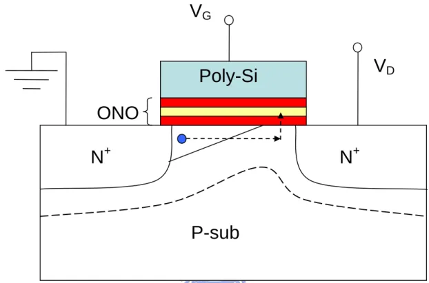
Devices used in this study were fabricated on 6-inch silicon wafers. First, silicon wafers were capped with a 1000Å silicon dioxide layer serving as the starting substrate. Then, a 1000Å n+-doped poly-Si layers was deposited on the starting substrate to serve as the gate electrode (side-gate electrode). The poly-Si layer was subsequently etched to form the gate stack. Afterwards, a total 210Å ONO multilayer gate dielectric, consisting of a 100Å-thick layer of tetra-ethyl-ortho-silicon (TEOS) blocking oxide at 700℃, a 55Å-thick layer of silicon nitride trapping layer at 780℃, and a 55Å-thick layer of TEOS tunneling oxide, all deposited by an Low Pressure Chemical Vapor Deposition (LPCVD) system. A 1000Å-thick amorphous-Si layer was then also deposited by LPCVD. Next, an annealing step was performed at 600℃ in N2 ambient for 24 hours to transform the amorphous-Si into poly-Si. Subsequently,
source/drain (S/D) implant was performed by P+ implantation at an energy of 15keV and a dose of 1x10-15 cm-2. Note that the implant energy was kept low so that most of the implanted dopants were located near the top surface of the poly-Si layer. S/D photoresist patterns were then formed on the substrate by a standard lithography step. A reactive plasma etch step was subsequently employed to remove the poly-Si layer except at the S/D regions, and the sidewall poly-Si nanowire channels were simultaneously formed in a self-aligned manner. After this step and subsequent
activation treatment, the S/D regions were formed with a heavy-dose implant. Note that, due to the low implantation energy, the nanowire channels remain undoped. Afterwards, the devices were divided into two splits, with one split fabricated is the double-gated configuration. In this split, 180Å-thick or 360Å-thick TEOS used as top gate oxide was deposited by LPCVD at 700℃. Subsequently, 1000Å n+
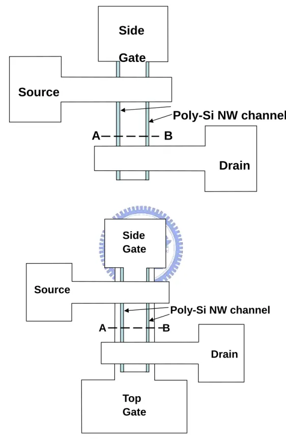
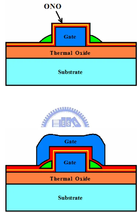
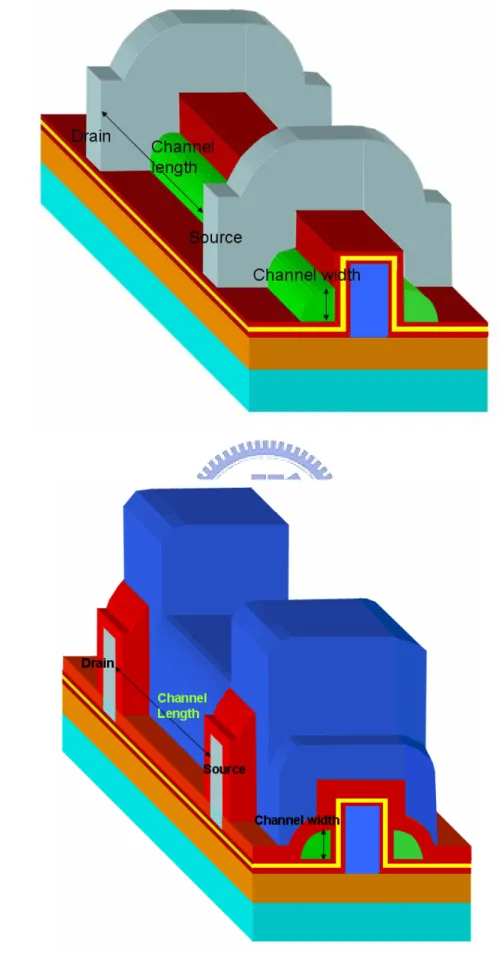
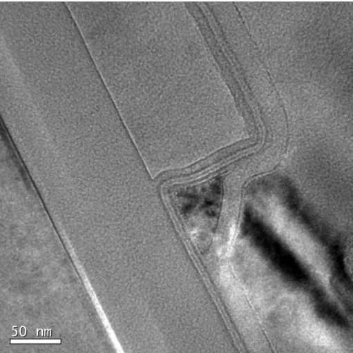
-doped poly-Si layers was deposited to serve as the gate electrode (top-gate). The other split with single-gated configuration skipped those steps until passivation deposition. All wafers then received the deposition of a 2000Å-thick passivation TEOS oxide layer by LPCVD at 700℃. Finally, the fabrication was completed after the formation of test pads using standard metallization steps. Top views of the single- and double-gated NW-SONOS are shown in Fig. 2-1(a) and Fig. 2-1(b), respectively. Fig. 2-2(a) and Fig. 2-2(b) respectively display the cross-sectional views along A-B in Fig. 2-1(a) and Fig. 2-1(b). The three-dimensional (3D) structures of the single- and double-gated NW-SONOS are illustrated in Fig. 2-3(a) and Fig. 2-3(b), respectively. The cross-sectional Transmission electron microscopy (TEM) picture of a double-gated NW-SONOS with 180Å-thick top gate oxide is shown in Fig. 2-4(a). The views shown in Fig. 2-4 indicate that the thickness and width of nanowire channel are around 65 nm and 45 nm, respectively.
2-2 The Program/Erase Mechanisms
In general, the program/erase mechanisms employed in SONOS include channel hot electron injection (CHEI), Fowler-Nordheim tunneling (FN tunneling) and band to band tunneling (BTBT). The three mechanisms will be illustrated and described in the following sub-sections.
2-2-1 Channel Hot Electron Injection
The channel hot electron injection can be well understood by “lucky-electron model” [34]. The injection of channel hot electrons into the gate oxide region occurs at large drain-to-source voltage, as illustrated schematically in Fig. 2-5. Electrons flowing from source to drain gain energy from the high-field region near the drain junction.
The electrons are emitted into the gate dielectric by first gaining enough energy without suffering an energy stripping collision in the channel and then being
redirected by acoustic phonon scattering toward the Si/oxide interface. On the other hand, the effective mass of hole is heavier than the electron. In addition, barrier height of valence band is also higher than conduction band. It is thus much more difficult for holes to obtain enough energy to surmount the oxide barrier. Therefore, hot-hole injection is rarely employed in nonvolatile memory operation.
Another merit of CHEI mechanism is to achieve NROM [35], SONOS with 2Bit/Cell. Employing CHEI, the charge can be programmed into drain or source terminals, then the data can be sensed by “reverse read”.
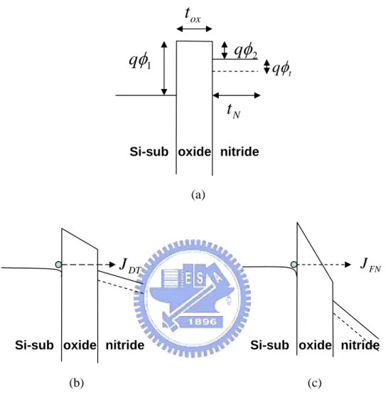
2-2-2 Fowler-Nordheim Tunneling
The tunneling mechanism is a kind of quantum-mechanical process during which the carriers may tunnel through the forbidden region of the insulator into the allowed states of the insulator or the opposite electrode material. Due to different electric field strength across the insulator, the tunneling mechanism can be classified into direct
tunneling and FN tunneling. If the electric field strength across the tunneling oxide
(E ) is smaller than ox ox
t qφ1
, where q is the barrier height between Si channel and φ1
tunneling oxide, the carriers may tunnel into nitride trapping layer by direct tunneling. The current density is expressed as:
ox E ox V B ox ox ox e V V AE J ⎥ ⎥ ⎥ ⎦ ⎤ ⎢ ⎢ ⎢ ⎣ ⎡ ⎟ ⎟ ⎠ ⎞ ⎜ ⎜ ⎝ ⎛ − − − ⎟⎟ ⎠ ⎞ ⎜⎜ ⎝ ⎛ − ⎟⎟ ⎠ ⎞ ⎜⎜ ⎝ ⎛ = 2 3 1 1 1 1 1 2 1 2 φ φ φ (eq. 2-1) where 1 2 3 8πhφ E q A= , hq m B ox b 3 2 8π φ32
= , and the electron effective mass, m , is ox
0.5m .Direct tunneling is illustrated in Fig. 2-6 (b). o
If E >ox ox
t qφ1
, the carriers may tunnel into nitride trapping layer by FN tunneling. The current density is expressed as:
Eox B oxe AE J − = 2 (eq. 2-2)
FN tunneling is illustrated in Fig. 2-6 (c). [36]
2-2-3 Band to Band Tunneling
The phenomenon of band to band tunneling occurs in the n+ drain region overlapping the gate. For this event to happen, the strength of electric field in the region must be sufficiently high to cause deep-depletion situation. Typically a negative gate voltage is applied, and the voltage difference between the gate and drain must be large. During the operation, electrons tunnel directly or are assisted by traps in the gap from valence band to conduction band at the drain. At the same time, holes are generated in the deep-depletion region, and are then accelerated by the strong field and may be attracted by the negative gate bias into the nitride trapping layer. The
Chapter 3
Basic Electrical Characteristics and
Program/Erase Characteristics
3-1 Basic Electrical Characteristics
3-1-1 Determination of The Threshold Voltage
For MOSFET, the threshold voltage (Vth) is usually determined from the
extrapolated gate voltage VGi by T Gi D2
V V
V = − , where VGi is determined by Gmmax.
However, this method is not suitable for TFTs. For TFTs, defects in grain boundary of the channel will trap the electrons, resulting in a rough Gm-VG curve under large VG
region. In this thesis, the method we adopted to determine Vth is the constant drain
current method in TFTs, i.e.,
Vth =VG |ID=1nA,VD=1V (eq. 3-1)
3-1-2 Comparisons of Transfer Characteristics
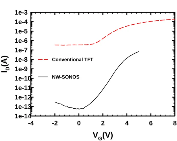
Fig. 3-1 shows transfer characteristics of conventional TFT and NW-SONOS. The subthreshold swing (SS) of NW-SONOS is significantly improved over that of the conventional TFT which can be ascribed to the high surface-to-volume ratio. In addition, the leakage current of NW-SONOS is much lower than that of the conventional TFT. The better SS and less leakage current will result in a larger programming window for the NW-SONOS. The merit demonstrates that NW-TFT is
more suitable than conventional TFT.
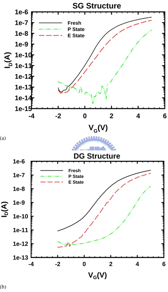
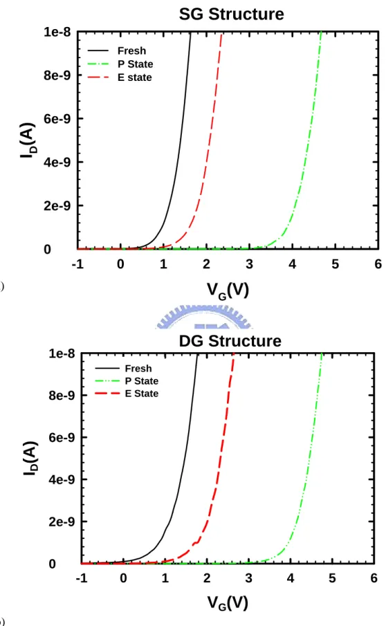
The fresh state, programming state, and erasing state of SG-NW-SONOS and DG-NW-SONOS are shown in Fig. 3-2 and Fig. 3-3. Fig. 3-2 (a) and Fig. 3-3 (a) show ID-VG curve in logarithmic scale, while Fig. 3-2 (b) and Fig. 3-3 (b) show ID-VG
curve in liner scale. From Fig. 3-2 and Fig. 3-3, it can be seen that Vth of erasing state
and fresh state is not equal. One plausible reason is that there are many deep-level traps existing in the channel and interface between the channel and dielectric layer. As device is programmed by applying a large bias, a considerable amount of electrons is gathered in the channel, and some electrons will be trapped in deep-level traps. Fig. 3-4 is in accord with the argument about deep-level traps. Because a fraction of electrons will be used to fill the traps at the first programming stage, the Vth shift of
the first programming stage is smaller than that after the second programming stage. In addition, the leakage current of erased state is smaller than that of fresh state in double-gated SONOS. Fig. 3-5 may explain this phenomenon. Figs. 3-5 (a) and (b) compare the leakage current of side-gate read mode relative to that of top-gate mode, It can be seen that the leakage current of the top-gate read mode is improved over the side-gate read mode. This demonstrates that the deep-level traps exist near not only the side-gate but also the top-gate, so electrons during the first programming stage are also trapped in deep-level traps near the top-gate.
3-2 Program/Erase Characteristics
In the study, the devices are programmed and erased by Fowler-Nordheim (FN) tunneling mechanism. In this structure, the conventional channel hot electron injetion (CHEI) method is not suitable because of the existence of the barrier height from
grain boundaries in the channel. The barrier height will hinder the acceleration of the electrons from the source to drain, hence the electrons will not be hot enough to inject into the trapping layer. For programming, both source and drain are grounded, and the gate is biased at a highly positive voltage to induce a strong electric field. And for erasing, source and drain are still grounded, and the gate is biased at a highly negative voltage to detrap electrons in the nitride. The bias of each electrode in figures is expressed as (side-gate, top-gate, drain, source) for both single-gated and double-gated SONOS (in single-gated SONOS, the bias of top-gate is always “0”). For example, (15, 15, 0, 0 ) means that the biases of side-gate (VSG) and top-gate (VTG)
are 15V, and the biases of drain (VD) and source (VS) are 0V. The program and erase
condition for single-gated SONOS and double-gated SONOS are listed at Table 3-1 and Table 3-2, respectively.
Vth shift versus programming time for side-gate bias of 13V, 14V, and 15V is
shown in Fig. 3-6. Fig. 3-6 (a) and Fig. 3-6 (b) show that the FN programming speeds of the single- and double-gated SONOS, respectively. It can be seen that memory window of around 2V can be achieved within 0.5 msec of programming time. The programming speed is shown to increase when applying a higher side-gate voltage. Fig. 3-7 shows the erasing characteristics of the single-gated SONOS and double-gated SONOS for side-gate bias of -10V, -12V, and -14V. The erasing speed is also found to increase with side-gate voltage. However, erase saturation may occur because gate injection is stronger at higher side-gate voltage. As decreasing the trapped charges in the nitride layer, the electric field across the tunneling oxide will also be reduced, and the electric field across the blocking oxide will be enhanced. Therefore, the electrons may be injected from the gate into the nitride, and the speed is larger than the erasing speed. In other words, when the erasing time is longer, the Vth may increase.
Fig. 3-8 and Fig. 3-9 show the programming speed and erasing speed versus channel length for single-gated SONOS and double-gated SONOS, respectively. The bias for programming is (15, 0, 0, 0 ) for each structure. Both the programming speed and the erasing speed change less with decreasing channel length. Furthermore, the short channel effect is improved due to high surface-to-volume ratio of nanowire.
Next, the influence of the VTG on the programming and erasing speed is discussed
in the following section. Programming speed and erasing speed for different VTG are
shown in Figs. 3-10 (a) and (b), respectively.
In programming, the programming speed is enhanced by the top-gate bias, with the maximum enhancement occurs at a top-gate bias of 3V. The Vth shift versus VTG is
shown in Fig. 3-11, where the programming time is 0.5msec and VSG is 15V. During
programming operation, there are a lot of electrons in the channel due to the side-gate bias, and both VS and VD are 0V, therefore, the voltage of the channel should be 0V. If
the top-gate is applied with positive voltage in programming situation, more electrons will be generated in the channel and the programming speed will be enhanced. However, with increasing VTG, the amount of electrons in the channel will reach
saturation, and the enhancement in the programming speed will stop. In addition, the electric field from large VTG may interfere with the electric field from VSG, thus
decreases the programming speed.
In erasing, the erasing speed is reduced by VTG. Vth shift versus VTG is shown in
Fig. 3-12. Since there may be no electrons due to the highly negative VSG, the channel
should be floating. And the influence of excess holes from VTG will be much less than
that due to the electric field from VTG.
Figs. 3-13 (a) and (b) show the effect of top-gate bias on Vth shift, i.e., VSG and
VS is 0V, VD is 1V, under programming and erasing operations, respectively. Only
charges trapping occurring in the top-gate oxide.
Figs. 3-14 (a) and (b) compare the programming speed and erasing speed of single-gated SONOS with those of double-gated SONOS, respectively. In our structure, the programming speed and erasing speed are not improved. Because the most important parameters that determine the programming speed and erasing speed are the thickness of tunneling oxide and the programming efficiency. But with the same thickness of tunneling oxide, the programming efficiency can not be enhanced obviously by double-gated structure with FN tunneling.
Chapter 4
Reliability Characteristics of TFT-SONOS
In addition to program/erase speed, nonvolatile memory cells have some important functional characteristics, which are used to evaluate the suitability and practicality of the cells under test. These characteristics are divided into two main classes, namely retention and endurance. They are discussed in the following sections.
4-1 Retention
Retention is a measure of the time that a nonvolatile memory cell can retain the charge in the trapping layer. Fig. 4-1 shows the band diagram for illustrating the charge loss paths in SONOS cells. There are two major leakage current components in relating to charge loss, one is the thermionic emission following Frenkel-Poole mechanism, another one is tunneling through either blocking oxide or tunneling oxide. The Frenkel-Poole emission is due to field-enhanced thermal excitation of trapped electrons into the conduction band of silicon. The trapped charge can be expressed as:
φ φ tτ t t t t t n e n( , )= ( ,0)• − (eq. 4-1)
where nt(φt,0)is the initial trapped charges, and τ is the time constant. The time
constant of Frenkel-Poole emission can be expressed as:
τFP =τ0exp{[φN −q(qE/πε)12]/kT} (eq. 4-2)
where φN is the corresponding nitride trap energy, E is the electric field and ε is the
high-frequency permittivity.
(T-T) tunneling, and band-to-trap (B-T) tunneling. The trapped electrons in nitride can tunnel back to the conduction band of the silicon substrate (trap-to-band tunneling), or to the interface traps between tunneling oxide and channel (trap-to-trap tunneling). In addition, holes from the silicon valence band may tunnel into the nitride traps under the influence of the internal electric field (band-to-trap tunneling). The time constant of tunneling mechanism can be expressed as:
τT =τ0⋅exp(αox⋅tox)⋅exp(αN ⋅tN) (eq. 4-3)
where t is the thickness of tunneling oxide, ox t is the distance from trap in nitride to N
tunneling oxide. Andτ0 , αox, and αN are different in trap-to-band tunneling,
trap-to-trap tunneling, and band-to-trap tunneling.[37]
Fig. 4-2 shows the data retention of single-gated NW-SONOS, and it is far worse than the required ten years retention. In general case, i.e., with single-crystal silicon for th channel and dry oxide for tunneling oxide, trap-to-trap tunneling is normally neglected for a fresh SONOS cell measurement. However, in our case with TFT-SONOS, since there are many interface traps existing between tunneling oxide fabricated by TEOS and poly-Si channel, trap-to-trap tunneling must be considered. Hence the worse retention capability for TFT-SONOS over conventional SONOS is expected. Nevertheless, as shown in Fig. 4-3, the data retention at programming state is improved by double-gated structure. Data retention with a continued electric field on the trapping layer is also tested. At the programming state, the side-gate is biased at -2V and the source and drain are grounded to accelerate the trapped charges loss. On the other hand, at the erasing state, the side-gate is biased at +2V and the source and drain are grounded to accelerate the charges tunneling into nitride. The result is shown in Fig. 4-4. The retention capability at programming state of double-gated structure is better than that of single-gated structure, and the erasing state of single gated structure is more easily influenced by electric field than that of double gated
one.
Possible cause of the phenomenon is the location of trapped charges. In equation 4-3, τT is seriously influenced byt . If the distance from the location of trapped N
charges to tunneling oxide is larger, nitride will retain the trapped charges longer. In addition, since the nitride layer covers the whole side-gate and no oxide layer stops the charges from diffusing toward the vertical dimension in our structure, the distance from the location of trapped charges to channel edge is important for retention. Based on the assumption, the cause of improved retention ability is due to the top-gate, which can change the direction of electric field toward trapping layer, and cause charges to be trapped deep.
If top-gate can change the direction of electric field toward trapping layer, different VTG will cause charges to be trapped on different locations. Therefore, the
retention will also be different. Retention under different VTG, i.e., VTG of 15V, 0V,
and floating, is compared in Fig. 4-5, and the result supports the assumption.
In addition, the Vth of single-gated structure (Vth, SG) is the smallest, while the Vth
of double-gated structure (Vth, DG) with 180Å-thick top gate oxide is the largest, as
shown in Fig. 4-4. The explanation of this situation is referred from [38]. Fig. 4-6 is extracted from [37], and State C in Fig. 4-6 (c) shows that when Vg2 is less than VthDG,
Vth(G1) will be larger than VthDG. Therefore, since VTG is grounded in read state, i.e.,
VTG is smaller than VthDG, Vth, SG is smaller than Vth, DG. Besides, when Tox2 is thinner,
DE AB
will be larger with the same ΔVg2. Hence, Vth, DG with 180Å-thick top gate oxide
is larger than that with 360Å-thick top gate oxide. In physics, VTG is lower than Vth, DG,
and the higher VSG is needed to generate sufficient electrons in the channel near the
side-gate to turn on the device, so Vth, SG will be higher. In addition, the thicker
will be smaller.
4-2 Endurance
Endurance is the ability of a nonvolatile memory to endure the damage of numerous cycles of programming and erasing, i.e., the number of erase/write cycles that the memory will retain the required memory window and continue to operate as specified in the data sheet. Since the carriers for programming and erasing have energy, they will cause the degradation of tunneling oxide and trapping layer in every operation. In addition, high electric field stress across tunneling oxide will increase the current density at low electric field. The excess current at low electric field is called stress-induced leakage current (SILC) [39]. SILC is attributed to stress-induced oxide defects, which lead to a trap assisted tunneling. The main parameters controlling SILC are the stress field, the amount of charge injected during the stress, and the oxide thickness.
In general, flash products are specified for 106 erase/program cycles. However, the endurance requirement can be loosened with the increase of memory density for the other applications. Fig. 4-7 shows the endurance requirement of NAND Flash memories [40]. We can see that the endurance requirement is 100k cycles for NAND Flash with 256 MB density. Since for a memory array with higher density, a certain cell in a block has less possibility of being written and erased. This is because the memory operation of an individual cell in the array is repeated only after the entire memory blocks are addressed. This is why the endurance requirement of digital still camera (DSC), the biggest NAND Flash application, has decreased from 10.3K cycles for 128MB to 2.6K cycles for 1GB. The endurance requirement is sufficient for the
user to take 700 photos with 1MB size every day for 10 years.
Figs. 4-8 (a) and (b) show the ID-VG curve of single-gated and double-gated
structures with increasing erase/program cycles. It can be seen that the subthreshold swing and memory window of both structures worsen with increasing erase/program cycles. The subthreshold swing worsening is due to the degradation of tunneling oxide, and the memory window closure is due to the degradation of nitride. Figs. 4-9 (a) and (b) show the memory window versus erase/program cycles of single-gated structure and double-gated structure, respectively. The poor endurance is due to the poor quality of TEOS for tunneling oxide and the horn of the channel. The traps are easily generated because of poor quality of TEOS. Besides, high electric field due to the horn of the channel will seriously damage the tunneling oxide.
Chapter 5
Conclusion and Future Work
5-1
Conclusion
In this thesis, we have successfully fabricated and characterized TFT-SONOS with nanowire structure. The nanowire channels were formed by sidewall spacer etching technique. The proposed fabrication method is simple, fast, and low cost. Moreover, we have also fabricated TFT-SONOSs with double-gated configuration and comparisons were made with their single-gated counterparts.
Regarding the programming speed and erasing speed, the characteristics of TFT-SONOS with nanowire structure are comparable to those of conventional SONOS. The double-gated configuration in the proposed device does not seem to contribute nor enhance the programming speed or erasing speed. On the other hand, the reliability of TFT-SONOS is still worse than that of the conventional SONOS, due to poor quality of tunneling oxide and the horn-shaped structure of the nanowire channels. However, the double-gated configuration is found to improve the retention of TFT-SONOS with nanowire structure. Although there are many disadvantages lying ahead and need to be improved, we demonstrate the feasibility of nonvolatile memory with nanowire-TFTs fabricated by the simple and production-worthy sidewall spacer technique.
5-2 Future Work
future. Since the poor reliability is due to the mediocre quality of tunneling oxide and the horn-shaped structure of the nanowire channels, some effective methods to alleviate these issues can be used for reliability improvement. One is to deposit high quality TEOS or replace the TEOS with another dielectric material with better quality. Another approach is to improve the nanowire structure by eliminating the horn or at least suppress its negative impact on the devices. In addition, further improvement in device characteristics is possible by introducing some advanced process techniques to improve the film crystallinity, such as laser annealing, metal induced lateral crystallization, and plasma treatment. We believe that dramatic progress in making such NW-SONOS device toward practical application will be made in the future with additional efforts to improve and optimize the device structure and process steps.
References
[1] H. C. Lin and S. M. Sze, “Nanoelectronic Technology: in Search of the
Ultimate Device Structure”, in Future Trends in Microelectronics: the Nano
Millennium, S. Luryi, J. M. Xu, and A. Zaslavsky, eds., pp. 4-14 (New York: Wiley 2004).
[2] X. Duan, Y. Huang, and C. M. Lieber, “Nonvolatile Memory and
Programmable Logic from Molecule-Gated Nanowires”, Nano Letters, Vol. 2,
No.5, pp. 487-490, 2002.
[3] X. Duan, C. Niu, V. Sahi, J. Chen , J. W. Parce, , S. Empedocles , and J. L. Goldman,“High-Performance Thin-Film Transistors Using Semiconductor Nanowires and Nanoribbons”, Nature, Vol.425, pp. 274-278, 2003.
[4] Yi Cui, Q. Wei, H. Park, and C. M. Lieber, “Nanowire Nanosensors for Highly
Sensitive and Selective Detection of Biological and Chemical Species”,
Science, Vol. 293, pp. 1289-1292, 2001.
[5] M. A. Thompson, E. J. Menke, C. C. Martens, and R. M. Penner, “Shrinking
Nanowires by Kinetically Controlled Electrooxidation”, J. Phys. Chem. B.,
Vol. 110, pp. 36-41, 2006.
[6] D. P. Yu, Z. G. Bai, Y. Ding, Q. L. Hang, H. Z. Zhang, J. J. Wang, Y. H. Zou, W. Qian, G. C. Xiong, H. T. Zhou, and S. Q. Feng, “Nanoscale silicon wires
synthesized using simple physical evaporation”, Appl. Phys. Lett., Vol. 72, pp.
3458-3460, 1998.
[7] H. C. Lin, M. H. Lee, C. J. Su, and S. W. Shen, “Fabrication and
Poly-Si Channels”, IEEE Trans. Electron Devices, Vol. 53, pp. 2471-2477,
2006.
[8] A. M. Morales and C. M. Lieber, “A Laser Ablation Method for the Synthesis
of Crystalline Semiconductor Nanowires”, Science, Vol. 279, pp. 208-211.,
1998.
[9] D. Wang, Q. Wang, A. Javey, R. Tu, H. Dai, H. Kim, P. C. McIntyre, T. Krishnamohan, and K. C. Saraswat, “Germanium Nanowire Field-Effect
Transistors with SiO2 and High-k HfO2 Gate Dielectrics”, Appl. Phys. Lett.,
Vol. 83, pp. 2432-2434, 2003.
[10] N. Wang, Y. F. Zhang, Y. H. Tang, C. S. Lee, and S. T. Lee, “SiO2-Enhanced
Synthesis of Si Nanowires by Laser Ablation”, Appl. Phys. Lett., Vol. 73, pp.
3902-3904, 1998.
[11] X. Duan, Y. Huang, Yi Cui, J. Wang, and C. M. Lieber, “Indium Phosphide
Nanowires as Building Blocks for Nanoscale Electronic and Optoelectronic Devices”, Nature, Vol. 409, pp. 66-69, 2001.
[12] Y. Huang, X. Duan, Q. Wei, and C. M. Lieber, “Directed Assembly of
One-Dimensional Nanostructures into Functional Networks”, Science, Vol.
291, pp. 630-633, 2001.
[13] A. Tao, F. Kim, C. Hess, J. Goldberger, R. He, Y. Sun, Y. Xia, and P. Yang
“Langmuir-Blodgett Silver Nanowire Monolayers for Molecular Sensing Using Surface-Enhanced Raman Spectroscopy”, Nano. Lett., Vol. 3, pp.
1229-1233, 2003.
[14] D. Kahng and S. M. Sze, “A Floating Gate and Its Application to Memory
Devices”, IEEE Trans. Electron Devices, Vol. 14, pp. 629-629, 1967.
[15] J. D. Blauwe, “Nanocrystal Nonvolatile Memory Devices”, IEEE Trans. on
[16] M. H. White, Y. Yang, A. Purwar, and M. L. French, “A Low Voltage SONOS
Nonvolatile Semiconductor Memory Technology”, IEEE Int’l Nonvolatile
Memory Technology Conference, 52 (1996).
[17] M. H. White, D. A. Adams, and J. Bu, “On the Go with SONOS”, IEEE
circuits & devices, pp. 22-31, 2000.
[18] H. E. Maes, J. Witters, and G. Groeseneken, “Trends in Non-Volatile Memory
Devices and Technologies”, Proc. 17 European Solid State Devices Res. Conf.
Bologna, pp. 743, 1987
[19] Y. N. Tan , W. K. Chim , W. K. Choi, M. S. Joo, and B. J. Cho, “Hafnium
Aluminum Oxide as Charge Storage and Blocking-Oxide Layers in SONOS-Type Nonvolatile Memory for High-Speed Operation” IEEE Trans.
Electron Devices, Vol. 53, pp. 654-662, 2006.
[20] K. K. Likharev, “Layered Tunnel Barriers for Nonvolatile Memory Devices”,
Appl. Phys. Lett., Vol. 73, pp. 2137-3139, 1998.
[21] B. Govoreanu, P. Blomme, M. Rosmeulen, J. V. Houdt, and K. D. Meyer,
“VARIOT: A Novel Multilayer Tunnel Barrier Concept for Low-Voltage Nonvolatile Memory Devices”, IEEE Trans. Electron Device Lett., Vol. 24, pp.
99-101, 2003.
[22] H. T. Lue, S. Y. Wang, E. K. Lai, Y. H. Shih, S. C. Lai, L. W. Yang, K. C. Chen, J. Ku, K. Y. Hsieh, R. Liu, and C. Y. Lu, “BE-SONOS: A Bandgap Engineered
SONOS with Excellent Performance and Reliability”, IEDM Tech. Dig., pp.
547- 550, 2005.
[23] H. T. Lue, S. Y. Wang, Y. H. Hsiao, E. K. Lai, L. W. Yang, T. Yang, K. C. Chen, K. Y. Hsieh, R. Liu, and C. Y. Lu, “Reliability Model of Bandgap Engineered
SONOS (BE-SONOS)”, IEDM 2006.
SONOS-type Memory with Double Tunnel Junction”, IEDM 2006.
[25] S. Cho, I. H. Park, T. H. Kim, J. S. Sim, K. W. Song, J. D. Lee, H. Shin, and B. G. Park, “Design and Optimization of Two-Bit Double-Gate Nonvolatile
Memory Cell for Highly Reliable Operation” IEEE Trans. on Nanotechnology,
Vol. 5, pp. 180-185, 2006.
[26] P. Xuan, M. She, B. Harteneck, A. Liddle, J. Bokor, and T. J. King, “FinFET
SONOS Flash Memory for Embedded Applications”, IEDM, Tech. Dig., pp.
609-612, 2003.
[27] J. R. Hwang, T. L. Lee, H. C. Ma, T. C. Lee, T. H. Chung, C. Y. Chang, S. D. Liu, B. C. Perng, J. W. Hsu, M. Y. Lee, C. Y. Ting, C. C. Huang, J. H. Wang, J. H. Shieh, and F. L. Yang, “20nm Gate Bulk-FinFET SONOS Flash”, IEDM,
Tech. Dig., pp. 154-157, 2005.
[28] M. Specht, R. Kommling, L. Dreeskornfeld, W. Weher, F. Hofmann, D. Alvarez, J. Kretz, R. J. Luyken, W. Rosner, H. Reisinger, E. Landgraf, T. Schulz, J. Hartwich, M. Stadele,V. Klandievski, E. Hartmann, and L. Risch, “Sub-40nm
Tri-Gate Charge Trapping Nonvolatile Memory Cells for High-Density Applications”, VLSI Tech. Dig., pp. 244-245, 2004.
[29] E. K. Lai, H. T. Lue, Y. H. Hsiao, J. Y. Hsieh, S. C. Lee, C. P. Lu, S. Y. Wang, L. W. Yang, K. C. Chen, J. Gong, K. Y. Hsieh, J. Ku, R. Liu, and C. Y. Lul, “A
Highly Stackable Thin-Film Transistor (TFT) NAND-Type Flash Memory”,
VLSI Tech. Dig., pp. 46-47, 2006.
[30] Y. H. Lin, C. H. Chien, T. H. Chou, T. S. Chao, C. Y. Chang, and T. F. Lei, “2-Bit
Poly-Si-TFT Nonvolatile Memory Using Hafnium oxide, Hafnium Silicate and Zirconium silicate”, IEDM, Tech. Dig., pp. 927-930, 2005.
[31] A. J. Walker, S. Nallamothu, E. H. Chen, M. Mahajani, S. B. Hemer, M. Clark, J. M. Cleeves, S. V. Dunton, V. L. Eckert, J. Gu, S. Hu, J. Knall, M. Konevecki, C.
Petti, S. Radigan, U. Raghuram, J. Vienna, and M. A. Vyvoda, “3D
TFT-SONOS Memory Cell for Ultra-High Density File Storage Applications”, VLSI Tech. Dig., pp. 29-30, 2003.
[32] H. Oshima and S. Morozumi, “Future Trends for TFT Integrated Circuits on
Glass Substrates”, IEDM Tech. Dig., pp.157, 1989.
[33] T. Serikawa, S. Shirai, A. Okamoto, and S. Suyama, “Low-Temperature
Fabrication of High-Mobility Poly-Si TFT’s for Large-Area LCD’s”, IEEE
Trans. Electron Devices, Vol. 36, pp. 1929-1933, 1989.
[34] C. Hu, “Lucky-electron model of channel hot electron emission”, IEDM, Vol.
25, pp. 22-25, 1979.
[35] B Eitan, P Pavan, I. Bloom, E. Aloni, A. Frommer, D. Finzi, “Can NROM, a
2-bit trapping storage cell, give a real challenge to floating gate cells?”,
SSDM, 1999.
[36] K. F. Schuegraf and C. Hu, “Hole Injection Si02 Breakdown Model for Very
Low Voltage Lifetime Extrapolation”, IEEE Trans. Electron Devices, pp.
761-767, Vol. 41, 1994
[37] Y. Yang, and M. H. White, “Charge Retention of Scaled SONOS Nonvolatile
Memory Devices at Elevated Temperatures”, Solid-State Electronics, Vol. 44,
pp. 949-958, 2000
[38] M. Masahara, Y. Liu, K. Sakamoto, K. Endo, T. Matsukawa, K. Ishii, T. Sekigawa, H. Yamauchi, H. Tanoue, S. Kanemaru, H. Koike, and E. Suzuki,
“Demonstration, Analysis, and Device Design Considerations for Independent DG MOSFETs”, IEEE Trans. Electron Devices, Vol. 52, pp.
2046-2053, 2005
[39] K. Naruke, S. Taguchi, and M. Wada, “Stress Induced Leakage Current
Dig., pp. 424-427, 1988.
[40] K. Kim and J. Choi, “Future Outlook of NAND Flash Technology for 40nm
Node and Beyond”, Non-Volatile Semiconductor Memory Workshop, pp. 9-11,
Side
Gate
Source
Drain
Poly-Si NW channel
A
B
(a)Side
Gate
Source
Drain
Poly-Si NW channel
A
B
Top
Gate
(b)(a)
(b)
(a)
(b)
P-sub
N
+N
+ONO
Poly-Si
V
DV
GFig. 2-5 Proposed trajectory of an emitted channel electron. An energetic electron is redirected toward the interface by an acoustic phonon scattering.
ox
t
1φ
q
q
φ
2 tq
φ
Nt
Si-sub oxide nitride
Si-sub oxide nitride Si-sub oxide nitride
DT
J
J
FN(a)
(b) (c)
Fig. 2-6 Energy band diagram of ONO structure and illustrations of the physical difference between Fowler-Nordheim and direct tunneling. (a) Energy band diagram of ONO at V=0, where q is barrier height between Si-channel φ1
and tunneling oxide, qφ2 is barrier height between tunneling oxide and
nitride, qφt is energy difference between the conduction band and trap
state of nitride, t and ox t are thickness of tunneling oxide and nitride N
respectively. (b) Direct tunneling is associated with transversal of a trapezoidal barrier. (c) Fowler-Nordheim Tunneling is associated with transversal of a triangular barrier.
VG < 0
(a)
(b)
ig. 2-7 Illustration of Band to band tunneling. (a) Breakdown occurs in the ir in F
deep-depletion layer in the n+ drain. (b) The path of electron-hole pa energy band diagram.
oxide nitride drain VD > 0 Poly-Si P-sub
N
+ N+ONO
Deep-deletion region +- -
( SG , X , D , S ) VSG(V) VTG(V) VD(V) VS(V) Time(s) Program Speed Test 13 ~ 15 X 0 0 1μs ~ 10ms Erase Speed Test -12 ~ -14 X 0 0 1μs ~ 1s Program for Reliability Test 15 X 0 0 0.5ms Erase for Reliability Test -12 X 0 0 50ms
Table 3-1. The program / erase condition for single-gated SONOS
( SG , TG , D , S ) VSG(V) VTG(V) VD(V) VS(V) Time(s) Program Speed Test 13 ~ 15 0 ~ 15 0 0 1μs ~ 10ms Erase Speed Test -12 ~ -14 0 ~ -5 0 0 1μs ~ 1s Program for Reliability Test 15 0 ~ 15 0 0 0.5ms Erase for Reliability Test -12 0 0 0 50ms
V
G(V)
-4
-2
0
2
4
6
8
I
D(A)
1e-14
1e-13
1e-12
1e-11
1e-10
1e-9
1e-8
1e-7
1e-6
1e-5
1e-4
1e-3
Conventional TFT NW-SONOSSG Structure
V
G(V)
-4
-2
0
2
4
6
1e-15
1e-14
1e-13
1e-12
1e-11
1e-10
1e-9
1e-8
1e-7
1e-6
Fresh P State E State(A)
DI
(a)DG Structure
V
G(V)
-4 -2 0 2 4 6I
D(A)
1e-13 1e-12 1e-11 1e-10 1e-9 1e-8 1e-7 1e-6 Fresh P State E State (b)Fig. 3-2 Fresh, programming state, and erasing state ID-VG curves under logarithmic
SG Structure
V
G(V)
-1 0 1 2 3 4 5 6I
D(A)
0 2e-9 4e-9 6e-9 8e-9 1e-8 Fresh P State E state (a)DG Structure
V
G(V)
-1 0 1 2 3 4 5 6I
D(A)
0 2e-9 4e-9 6e-9 8e-9 1e-8 Fresh P State E State (b)Fig. 3-3 Fresh, programming state, and erasing state ID-VG curves under linear scale
Programming Time (s)
1e-6
1e-5
1e-4
1e-3
1e-2
Δ
V
th
(V)
0.0
0.5
1.0
1.5
2.0
2.5
3.0
1st program 2nd programFig. 3-4 Programming characteristics of NW-SONOS after first and second programming.
V
G(V)
-4 -2 0 2 4 6I
D(A)
1e-13 1e-12 1e-11 1e-10 1e-9 1e-8 1e-7 1e-6Fresh of SG read mode Fresh of TG read mode
Fig. 3-5 (a) Fresh ID-VG curve of side-gate read and top-gate read modes.
V
G(V)
-4 -2 0 2 4 6I
D(A)
1e-13 1e-12 1e-11 1e-10 1e-9 1e-8 1e-7 1e-6E State of SG read mode E State of TG read mode
(a)
Programming Time(s)
1e-6
1e-5
1e-4
1e-3
1e-2
Δ
V
th
(V
)
0.0
0.5
1.0
1.5
2.0
2.5
3.0
3.5
P(13,X,0,0) SG P(14,X,0,0) SG P(15,X,0,0) SGProgramming Time(s)
1e-6
1e-5
1e-4
1e-3
1e-2
Δ
V
th
(V)
0.0
0.5
1.0
1.5
2.0
2.5
3.0
P(13,0,0,0) DG P(14,0,0,0) DG P(15,0,0,0) DG (b)Fig. 3-6 Programming characteristics of (a) single-gated (b) double-gated SONOS with different side-gate biases.
(a)
Erasing Time(s)
1e-6
1e-5
1e-4
1e-3
1e-2
1e-1
1e+0
Δ
V
th
(V)
-3.5
-3.0
-2.5
-2.0
-1.5
-1.0
-0.5
0.0
E(-10,X,0,0) SG E(-12,X,0,0) SG E(-14,X,0,0) SG (b)Erasing Time(s)
1e-6
1e-5
1e-4
1e-3
1e-2
1e-1
1e+0
Δ
V
th
(V)
-3.5
-3.0
-2.5
-2.0
-1.5
-1.0
-0.5
0.0
E(-10,0,0,0) DG E(-12,0,0,0) DG E(-14,0,0,0) DGFig. 3-7 Erasing characteristics of (a) single-gated (b) double-gated SONOS with different side-gate biases.
(a)
Programming Time(s)
1e-6
1e-5
1e-4
1e-3
1e-2
Δ
V
th
(V)
-0.5
0.0
0.5
1.0
1.5
2.0
2.5
3.0
3.5
P(15,X,0,0) SG, L=0.8μm P(15,X,0,0) SG, L=1.0μm P(15,X,0,0) SG, L=1.5μm P(15,X,0,0) SG, L=2.0μmErasing Time(s)
1e-6
1e-5
1e-4
1e-3
1e-2
1e-1
1e+0
Δ
V
th
(V)
-3.5
-3.0
-2.5
-2.0
-1.5
-1.0
-0.5
0.0
E(-12,X,0,0) SG, L=0.8μm E(-12,X,0,0) SG, L=1.0μm E(-12,X,0,0) SG, L=1.5μm E(-12,X,0,0) SG, L=2.0μm (b)Fig. 3-8 (a) Programming and (b) erasing characteristics of single-gated SONOS with different channel lengths.
Programming Time(s)
1e-6
1e-5
1e-4
1e-3
1e-2
Δ
V
th
(V)
0.0
0.5
1.0
1.5
2.0
2.5
3.0
P(15,0,0,0) DG, L=0.8μm P(15,0,0,0) DG, L=1.0μm P(15,0,0,0) DG, L=1.5μm P(15,0,0,0) DG, L=2.0μm (a) (b)Erasing Time(s)
1e-6
1e-5
1e-4
1e-3
1e-2
1e-1
1e+0
Δ
V
th
(V)
-3.5
-3.0
-2.5
-2.0
-1.5
-1.0
-0.5
0.0
E(-12,0,0,0) DG, L=0.8μm E(-12,0,0,0) DG, L=1.0μm E(-12,0,0,0) DG, L=1.5μm E(-12,0,0,0) DG, L=2.0μmFig. 3-9 (a) Programming and (b) erasing characteristics of double-gated SONOS with different channel lengths.
Programming Time(s)
1e-6
1e-5
1e-4
1e-3
1e-2
Δ
V
th
(V)
0
1
2
3
4
P(15, 0,0,0) DG P(15, 1,0,0) DG P(15, 3,0,0) DG P(15, 5,0,0) DG P(15,15,0,0) DG (a) (b)Erasing Time(s)
1e-6
1e-5
1e-4
1e-3
1e-2
1e-1
1e+0
Δ
V
th
(V)
-4
-3
-2
-1
0
E(-12, 0,0,0) DG E(-12, -1,0,0) DG E(-12, -3,0,0) DG E(-12, -5,0,0) DGFig. 3-10 (a) Programming and (b) erasing characteristics of double-gated SONOS with different top-gate biases.
VTG(V)
0
1
3
5
15
Δ
V
th
(V)
2.0
2.2
2.4
2.6
2.8
3.0
Fig. 3-11 Vth shift of double-gated SONOS at programming time = 0.5msec,
VTG(V)
0
-1
-2
-3
Δ
V
th
(V)
-2.6
-2.4
-2.2
-2.0
-1.8
-1.6
Fig. 3-12 Vth shift of double-gated SONOS at erasing time = 0.5msec, side-gate
(a)
Programming Time(s)
1e-6 1e-5 1e-4 1e-3 1e-2
Δ
V
th
(V)
-1.0 -0.5 0.0 0.5 1.0 P(15, 0,0,0)Erasing Time(s)
1e-6
1e-5
1e-4
1e-3
1e-2
1e-1
1e+0
Δ
V
th
(V)
-1.0
-0.5
0.0
0.5
1.0
E(-12, 0,0,0) (b)Fig. 3-13 (a) programming and (b) erasing characteristics of double-gated SONOS under top-gate read mode, i.e., ΔVth is the Vth shift of top-gate.
(a)
Programming Time(s)
1e-6
1e-5
1e-4
1e-3
1e-2
Δ
V
th
(V)
0
1
2
3
4
P(15, 0,0,0) SGP(15, 7,0,0) DG with 36nm Top oxide P(15, 3,0,0) DG with 18nm Top oxide
Erasing Time(s)
1e-6
1e-5
1e-4
1e-3
1e-2
1e-1
1e+0
Δ
V
th
(V
)
-4
-3
-2
-1
0
1
E(-12, 0,0,0) SGP(-12, -5,0,0) DG with 36nm Top oxide P(-12, -3,0,0) DG with 18nm Top oxide
(b)
Fig. 3-14 Comparisons of (a) programming and (b) erasing characteristics between single-gated SONOS and double-gated SONOS.
Fig. 4-1 Band diagram of trapped charge loss path in SONOS: trap-to-band
(B-T), tunneling (TB), trap-to-trap tunneling (T-T), band-to-trap tunneling
thermal excitation (TE) and Frenkel-Poole emission (PF).
T-B T-T B-T TE FP Nitride Tunneling oxide Blocking oxide Gate Channel e q
φ
1 e qφ
2 h qφ
1 h qφ
2 Ttox TN Tboxig. 4-2 Retention characteristics of single-gated SONOS. F