具有高介電係數閘極介電層之薄膜電晶體製作及特性研究
121
0
0
全文
(2) 具有高介電係數閘極介電層 之薄膜電晶體製作及特性研究 Fabrication and Characterization of Thin-Film Transistors With High-κ Gate Dielectrics 研 究 生:鄧 至 剛. Student:Chih-Kang Deng. 指導教授:邱 碧 秀 博士. Advisor:Dr. Bi-Shiou Chiou. 國 立 交 通 大 學 電子工程學系 電子研究所 博 士 論 文 A Dissertation Submitted to Department of Electronics Engineering and Institute of Electronics College of Electrical and Computer Engineering National Chiao Tung University in partial Fulfillment of the Requirements for the Degree of Doctor of Philosophy in Electronics Engineering. June 2009 Hsinchu, Taiwan, Republic of China. 中 華 民 國 九 十 八 年 七 月.
(3) 具有高介電係數閘極介電層 之薄膜電晶體製作及特性研究 研 究 生:鄧 至 剛. 指導教授:邱 碧 秀 博士 國 立 交 通 大 學 電子工程學系 電子研究所 摘. 要. 在本論文中提出整合高介電係數閘極介電層製程,來改善低溫複晶矽薄膜電晶體以 及有機五環素薄膜電晶體的特性。首先提出具有高介電係數氧化鐠閘極介電層的低溫固 相再結晶複晶矽薄膜電晶體,並且在施行固相再結晶退火前,對非晶化矽薄膜進行氮離 子植入。結果顯示,在一定濃度的氮離子植入非晶化矽情況下,能夠在固相再結晶的退 火過程中,修補晶粒邊界的缺陷態位,進而大幅改善低溫複晶矽薄膜電晶體元件的電 性,而且此氮離子修補技術亦可在低溫複晶矽薄膜裡形成較強的矽-氮鍵結,來取代一 般較弱的矽-矽鍵結和矽-氫鍵結,來增進元件對熱載子效應的免疫力。另一方面,使用 具有高介電係數的氧化鐠閘極介電層,能夠在相同的等效氧化層厚度下,得到較大的閘 極電容密度,加強電晶體閘極的控制能力,使複晶矽通道區產生更多的少數載子,迅速 填滿補晶粒邊界的缺陷態位,以致於能大幅地改善薄膜電晶體的臨界電壓、次臨界斜率 等電性。第二部分,對於有機五環素薄膜電晶體,我們也整合具有高介電係數的氧化鑭 釔閘極介電層,預期得到良好的電性結果。結果顯示,高介電係數的氧化鑭釔的閘極介 電層,具有高的閘極電容密度和低的閘極漏電流,能夠讓有機薄膜電晶體的五環素通 道,在飽和累積工作區間的操作下,成功誘導產生更多的累積載子,來大幅降低有機薄 膜電晶體的操作電壓至兩伏特內。因此,整合高介電係數閘極介電層的薄膜電晶體,將 會符合往後顯示器科技的發展趨勢,適合在高速元件或低電壓操作電路的應用。. i.
(4) Fabrication and Characterization of Thin-Film Transistors With High-κ Gate Dielectrics Student:Chih-Kang Deng. Advisor:Dr. Bi-Shiou Chiou. Department of Electronics Engineering and Institute of Electronics College of Electrical and Computer Engineering National Chiao-Tung University. Abstract In this thesis, we integrate high dielectric constant (high-κ) materials as gate dielectrics to improve the electrical performances of the low-temperature polycrystalline silicon (LTPS) thin-film transistor (TFT) and the pentacene-based organic TFT (OTFT). First, we study the LTPS TFT with a high-κ praseodymium oxide (Pr2O3) gate dielectric and incorporating with nitrogen implantation before solid-phase crystallization (SPC) annealing. Nitrogen atoms with appropriate dosages of 5 × 1012 cm-2 implanted into amorphous silicon (α-Si) film could passivate the trap states in grain and in grain boundaries during SPC annealing and greatly improve electrical performances. This nitrogen modification could form the strong Si-N bonds in place of the weak Si-Si and Si-H bonds to enhance the immunity against hot-carrier stress. Besides, using Pr2O3 as a gate insulator could obtain a thin equivalent-oxide thickness (EOT) of 8 nm and a high gate capacitance density of 432 nF/cm2 with well gate controllability, compared to conventional tetraethoxylsilane (TEOS) oxide. Because the poly-Si channel could induce more minority carriers to quickly fill up trap states in grain boundaries, the threshold voltage and the subthreshold swing of the LTPS TFT could be greatly improved by integrating high-κ gate dielectrics. Second, we also demonstrated the pentacene-based OTFT with a high-κ lanthanum-yttrium oxide (LaYOX) gate dielectric to ii.
(5) achieve high-performance characteristics. The results show that the 30-nm LaYOX film as the gate insulator of the OTFT device exhibits a high capacitance density of approximate 410 nF/cm2 and a low leakage current below 20 nA/cm2 biased at −4 V. It could induce more accumulation charges in the pentacene channel layer to obtain good device performances, such as a low threshold voltage of 1.25 V, a low subthreshold swing of 265 mV/Dec., and a field-effect mobility of 0.22 cm2/V-s, under the 2-V low-voltage operation. Therefore, these TFT devices with high-κ gate dielectrics integration are suitable for high-speed or low-voltage electronic applications in flat panel display (FDP) field in the near future.. iii.
(6) ACKNOWLEDGEMENTS Firstly, I would like to express my sincere gratitude to my supervisor, Prof. Bi-Shiou Chiou, for her guidance, support, and encouragements, in my last-three years of my graduate life. She not only authorized to me in my research work but modified my impulsive temper to others. Thus, I could entirely concentrate on my studies and upgrade professional knowledge in various semiconductor fields. Special thanks for valuable comments and criticisms of my defense committee who let me have opportunities to correct and improve my dissertation. I have met many nice professors and dear friends in my long-term pursing degrees days in National Chiao-Tung University. I am indebted to Prof. Kow-Ming Chang and Prof. Chung Tasi, who opened my initial way on semiconductor research field. I also thank Prof. Ker for teaching me technical writing skills even if there were many boring chores and projects I dealt with everyday. And then, I would like to thank my colleagues in CBS Lab., including Dr. Lisa Chang, Dr. C.-C. Ho, and Miss S.-W. Wu, for many discussions and experiences related to my research work. I am further indebted to OLED Lab., including Black-Man, A-Wen, Chunggod, Small-P, and Robert, where so much fun I got. For maintaining a fine and convenient experiment environment, I wish to thank K. Pong, S.-L. Hsu. R.-T. Chen, S.-L. Fan, G.-H. Huang, and Omnipotent God-Chin in Nano Facility Center as well as Sun Chaio, T.-W. Fan, and T.-F. Hsu in Nano Device Laboratory. Thank One-One, Han-Yu, Ming-Fong, and Bu-Bu for their great help on electric fields. Thank Raymond and Cheng-Cheng, who could console with each other, being reproved by our Bosses in hysteria. It was too late to thank my angel Lien who brought me here. If there was anyone lost in previous list, forgave my incautious and I expressed my honest gratitude to my all friends again. At last, I would show my deepest appreciation to my wonderful family. With their continuous love and support, my research work has a perfect ending, and it is dedicated to my beloved parents, Mr. Guang-Cyuan Deng and Mrs. Jin-Mei Huang.. iv.
(7) Contents Abstract (Chinese) ---------------------------------------------------------------------------------. i. Abstract (English) ----------------------------------------------------------------------------------. ii. Acknowledgements (English) --------------------------------------------------------------------. iv. Contents ----------------------------------------------------------------------------------------------. v. List of Tables ----------------------------------------------------------------------------------------. viii. Figures Caption ------------------------------------------------------------------------------------. ix. Chapter 1 Introduction -------------------------------------------------------------------------. 1. General Background and Literatures Review --------------------------------. 9. 2.1 Active-Matrix Liquid Crystal Display Technology --------------------------------. 9. 2.2 History of Thin-Film Transistors -----------------------------------------------------. 11. 2.3 Organic Semiconductor Materials ----------------------------------------------------. 13. 2.4 Solid-Phase Crystallization Technology ---------------------------------------------. 15. 2.5 The Properties of High-κ Materials --------------------------------------------------. 17. 2.5-1 Characteristics of Praseodymium Oxide -----------------------------------. 18. 2.5-2 Characteristics of Lanthanum-Yttrium Oxide -----------------------------. 19. 2.6 Review on High-κ Materials Used in Thin-Film Transistors ---------------------. 20. 2.7 Current Equations of Thin-Film Transistors ----------------------------------------. 22. Chapter 2. 2.7-1 Drain Current Equations in Linear and Saturation Regions --------------. 22. 2.7-2 Drain Current Equations in Subthreshold Region -------------------------. 23. 2.7-3 Drain Current Equations of Organic Thin-Film Transistors -------------. 24. v.
(8) Chapter 3. Fabrication and Characterization Methods ----------------------------------. 38. 3.1 Fabrication of Low-Temperature Polycrystalline silicon Praseodymium Oxide Thin-Film Transistors With Various Nitrogen Dosages ----------------------------. 38. 3.2 Fabrication of Pentacene-Based Organic Thin-Film Transistors With Lanthanum-Yttrium Oxide ------------------------------------------------------------. 42. 3.3 Thermal Evaporation and Electron-Beam Evaporation ----------------------------. 44. 3.4 Device Measurement and Parameter Extraction ------------------------------------. 46. 3.5 Material Analysis -----------------------------------------------------------------------. 50. Results and Discussion ------------------------------------------------------------. 59. Chapter 4. 4.1 Properties of Low-Temperature Polycrystalline Silicon Praseodymium Oxide Thin-Film Transistors With Various Nitrogen Dosages ----------------------------. 60. 4.1-1 Characteristics of Pr2O3 MIS Capacitors -----------------------------------. 60. 4.1-2 Characteristics of Pr2O3 Poly-Si TFTs With Nitrogen Implantation-----. 61. 4.1-3 Summary ------------------------------------------------------------------------. 66. 4.2 Properties of Pentacene-Based Organic Thin-Film Transistors With Lanthanum-Yttrium Oxide ------------------------------------------------------------. 67. 4.2-1 Characteristics of LaYOX MIM Capacitors --------------------------------. 67. 4.2-2 Characteristics of Pentacene Layer ------------------------------------------. 68. 4.2-3 Characteristics of OrganicTFTs With LaYOX Gate Insulator ------------. 69. 4.2-4 Summary ------------------------------------------------------------------------. 73. Conclusion and Future Prospects -----------------------------------------------. 87. 5.1 Conclusion -------------------------------------------------------------------------------. 87. 5.2 Future Prospects -------------------------------------------------------------------------. 88. Chapter 5. vi.
(9) References -------------------------------------------------------------------------------------------. 90. Vita (English) ---------------------------------------------------------------------------------------. 104. Publication List ------------------------------------------------------------------------------------- 105. vii.
(10) List of Tables. Table 1-1. The roadmap of system integration trend of FPD provided by Sony Corporation [1]. --------------------------------------------------------------------------------------------. Table 2-1. 6. Comparison on electrical characteristics of SPC poly-Si TFTs with various gate dielectrics, including TEOS oxide, ONO stack oxide, nitrous oxide (N2O), aluminum oxide (Al2O3), lanthanum-aluminum oxide (LaAlO3), and hafnium oxide (HfO2). -------------------------------------------------------------------------------. Table 2-2. 36. Comparison on electrical characteristics of pentacene-based organic TFTs with various gate dielectrics, including silicon oxide (SiO2), barium zirconate titanate (BZT),. gadolinium. oxide. (Gd2O3),. tantalum. pentoxide. (Ta2O5),. lanthanum-aluminum oxide (LaAlO3), titanium oxide (TiO2), Mn-doped barium strontium titanate (Mn-BST), and titanium-silicon oxide (TiSiO). ------------------ 37 Table 4-1. The relationships between trap states and device parameters of LTPS TFTs. -----. Table 4-2. Comparison on electrical parameters of SPC poly-Si TFTs with various gate dielectrics,. including. TEOS. oxide,. aluminum. oxide. (Al2O3),. lanthanum-aluminum oxide (LaAlO3), and praseodymium oxide (Pr2O3). -------Table 4-3. 77. 81. Comparison on electrical characteristics of pentacene-based organic TFTs with various gate dielectrics, including silicon oxide (SiO2), barium zirconate titanate (BZT), gadolinium oxide (Gd2O3), tantalum pentoxide (Ta2O5), titanium oxide (TiO2), and lanthanum-yttrium oxide (LaYOX). ---------------------------------------. viii. 86.
(11) Figures Caption. Fig. 1-1. The applications of flat panel displays (FPDs) in our daily lives. -------------------. 6. Fig. 1-2. The applications of organic thin-film transistor (OTFT) on flexible electronics. -. 7. Fig. 1-3. The methods to improve characteristics of low-temperature polycrystalline silicon (LTPS) thin-film transistor (TFT). ----------------------------------------------. 7. Fig. 1-4. The methods to improve characteristics of organic thin-film transistor (OTFT). -. 8. Fig. 1-5. Organic materials used as active channel layers for organic thin-film transistors (OTFTs). [21]. ------------------------------------------------------------------------------. Fig. 2-1. 8. Cross-sectional view of a unit pixel in active-matrix liquid crystal display 27 (AMLCD) [26]. -----------------------------------------------------------------------------. Fig. 2-2. The equivalent circuitry for the addressing matrix of an AMLCD [27]. ------------ 27. Fig. 2-3. Schematic diagram of Weimer’s CdS TFT with top-gate staggered structure [28]. 28. Fig. 2-4. Schematic diagram of LeComber’s amorphous silicon (α-Si) TFT structure and its transfer characteristics [30]. ----------------------------------------------------------. Fig. 2-5. Schematic cross section of an α-Si TFT with the “etch-stopper” layer and the in-situ tri-layer [32]. -----------------------------------------------------------------------. Fig. 2-6. 28. Schematic cross section of a top-gate low-temperature polysilicon TFT with a storage capacitor [34]. ---------------------------------------------------------------------. Fig. 2-7. 28. 29. Schematic of the geometries frequently used in organic thin-film transistors with (a) inverted-staggered structure, and (b) inverted-coplanar structure [44]. --------- 29. Fig. 2-8. The output characteristic and the transfer characteristic of the pentacene-based organic thin-film transistor with a high saturation mobility of 0.62 cm2/V-s [46].. Fig. 2-9. 29. The energy levels of oligo-thiophenes and poly-thiophenes as a function of the number of conjugated units [48]. --------------------------------------------------------- 30. ix.
(12) Fig. 2-10. Commonly used high-performance organic and polymer semiconductor materials [21]. ------------------------------------------------------------------------------. Fig. 2-11. Schematic of the re-crystallization mechanism for solid phase growth of amorphous silicon (α-Si) [52]. -----------------------------------------------------------. Fig. 2-12. 31. Summarized alternative high-κ gate dielectric materials reported in VLSI Symposium and IEDM from 1999 to 2005. --------------------------------------------. Fig. 2-14. 31. TEM micrographs for amorphous silicon (α-Si) film as a function of annealing time, such as as-deposited, 1HR, 2HR, and 24HR [53]. ------------------------------. Fig. 2-13. 30. 32. Energy bandgap versus dielectric constant plots for candidate gate insulators [62], [63]. ------------------------------------------------------------------------------------ 32. Fig. 2-15. Energy bandgap versus various lanthanide oxides [67], [68]. ------------------------ 33. Fig. 2-16. Dependence of mobility (μ) on gate electric field (E). (b) Dependence of channel mobility (μ) on charge density (QS). Black or white sample correspond to channel mobility (μ) calculated from gate sweep or drain sweep, respectively. 500 nm SiO2 with gate sweeps (o); 120 nm SiO2 with gate sweeps (•); 82 nm BST with drain sweeps (♠); 90 nm BST with gate sweeps ( Δ ); 122 nm BZT with drain sweeps (); 128 nm BZT with gate sweeps (□) [25]. ------------------- 33. Fig. 2-17. Schematic view of a thin-film transistor (TFT) under gate and drain biases [93].. Fig. 2-18. The energy bandgap diagram of the metal-insulator-semiconductor (MIS) structure under gate bias [93]. ------------------------------------------------------------. Fig. 2-19. 34. 34. Schematic view of an organic thin-film transistor (OTFT) working in accumulation region under high drain bias [95]. --------------------------------------- 35. Fig. 3-1. The main process steps of the Pr2O3 poly-Si TFT with nitrogen-implanted poly-Si film. (a) Thermal oxidation, α-Si deposition, nitrogen implantation, and SPC annealing. (b) Active region patterning, Pr2O3 deposition, and Pr2O3. x.
(13) annealing. (c) TaN gate deposition and patterning, and then self-align implantation and activation. (d) ILD deposition and contact hole opening. (e) Al deposition and patterning. ----------------------------------------------------------------- 53 Fig. 3-2. (a) The top view of the fabricated pentacene-based organic thin-film transistor (OTFT). (b) The cross-sectional structure of the pentacene OTFT with high-κ LaYOX gate insulator along AA’ dashed line in (a). -----------------------------------. Fig. 3-3. 54. The schematic view of the shadow masks corresponding to their process. (a) Shadow mask 1 for TaN gate deposition. (b) Shadow mask 2 with the TaN pattern alignment for high-κ LaYOX deposition. (c) Shadow mask 3 with the TaN pattern alignment for pentacene deposition. (d) Shadow mask 4 with the TaN pattern alignment for Au electrode deposition. ----------------------------------- 56. Fig. 3-4. The schematic view of the Au/LaYOX/TaN metal-insulator-metal (MIM) capacitors in-situ fabricated with OTFT device. ---------------------------------------. Fig. 3-5. The schematic views of (a) the thermal evaporation system, and (b) the electron-beam evaporation system. ------------------------------------------------------. Fig. 3-6. 57. The device parameters, including threshold voltage (VTH), subthreshold swing (S.S), and ON/OFF current ratio, extracted from the transfer characteristic plot. -. Fig. 4-1. 56. 58. The C-V characteristic and the leakage current density of the Pr2O3 film on Si substrate. The insert is the cross-sectional TEM image of the proposed Pr2O3 poly-Si TFT. --------------------------------------------------------------------------------. Fig. 4-2. 74. The XPS spectra of Pr 3d and O 1s core level for the Pr2O3 gate insulator on Si substrate. ------------------------------------------------------------------------------------- 75. Fig. 4-3. The transfer characteristics of the Pr2O3 poly-Si TFTs with various nitrogen dosages of zero (control sample), 5 × 1012 cm-2, and 5 × 1013 cm-2 under VDS = 0.1 V. -----------------------------------------------------------------------------------------. xi. 76.
(14) Fig. 4-4. The transfer characteristics (IDS−VGS) of the Pr2O3 poly-Si TFTs with nitrogen dosages of zero and 5 × 1012 cm-2 under VDS = 0.1 V and 1 V. The inset is the table of the electrical parameters. --------------------------------------------------------. Fig. 4-5. The output characteristics (IDS−VDS) of the Pr2O3 poly-Si TFTs with nitrogen dosages of 0 cm-2 and 5×1012 cm-2. ------------------------------------------------------. Fig. 4-6. 78. 79. The drain current degradation for the Pr2O3 poly-Si TFTs with and without nitrogen implantation under hot-carrier stress condition. ----------------------------- 80. Fig. 4-7. The capacitance-voltage (C−V) and the current density-voltage (J−V) characteristics of the Au/LaYOX/TaN MIM capacitor. -------------------------------- 82. Fig. 4-8. The glancing-incidence X-ray diffraction (GI-XRD) spectra and the atomic force microscopy (AFM) image (inset) of pentacene channel layer deposited on the LaYOX/TaN gate structure. ---------------------------------------------------------------. Fig. 4-9. 83. Transfer characteristics (IDS−VGS) and its square root plot (IDS1/2−VGS) of the pentacene-based organic thin-film transistor with a high-κ dielectric of LaYOX gate insulator at VDS = −2 V. --------------------------------------------------------------. Fig. 4-10. 84. The output characteristics (IDS−VDS) of the pentacene-based organic thin-film transistor with a high-κ dielectric of LaYOX gate insulator. -------------------------. xii. 85.
(15) CHAPTER 1 INTRODUCTION Over the past ten years, flat panel displays (FPDs) have became frequent features to provide any instantaneous information in our daily lives, for examples, mobile phones, personal digital assistants (PDAs), notebooks, desktop computer monitors, televisions (TVs) etc, as shown in Fig. 1-1. They replace traditionally heavy cathode ray tube (CRT) and develop toward thin short in portable device or large-scale display. Today, the business of the display industry and its derivative marketing are significantly growing up and gradually catching up those of the semiconductor industry and the automobile industry. For high definition (HD), high quality, portable, power saving, and low-cost considerations, the fabrications of FPD technology must make new breakthroughs to satisfy human being’s pursing. One of the breakthroughs is to improve the electrical performance of the thin-film transistor (TFT) device with a higher driving capability. A TFT device with a higher driving capability could use a smaller device dimension to drive liquid crystal (LC) in active matrix region, hence achieving a higher aperture ratio (AR) and a higher definition. Besides, it also could be directly embedded functional and control circuits by in-situ fabricated active-matrix TFT. devices. on. peripheral. panel. without. extra. tap-automated-bounding. (TAB). integrated-circuit (IC) to reduce the cost of the backend process on FPD. Table 1-1 shows the roadmap proposed by Nakajima of Sony Corporation for integrating the circuit system into FPD to realize system-on-glass (SOG) or system-on-panel (SOP) concept [1]. By using the index of low-temperature polycrystalline silicon (LTPS) technology, the mobility is enhanced from 50 cm2/V-s to 200 cm2/V-s, the design rule of the channel length is shrunk from 3.5 μm to 1 μm, and the threshold voltage is decreased from 2 V to 0.5 V. Because of the improvement of TFT device performance, many kinds of integrated circuit -1-.
(16) function on panel could migrate from analog driving circuits in 1st generation, digital-to-analog converter (DAC) circuits in 2nd generation, interface signal control circuits in 3rd generation, and finally to central processing unit (CPU) and memory circuits in 4th generation. In the near future, the FPD is not only for displaying information but also for increasing added value of digital and mobile products with high performance. Although these prototypes have been announced by lots of international FPD companies, they still need a period of time appearing in production line. Hence, how to improve electrical performance of a unit TFT device has became a research emphasis. Although pursing high performance of LTPS TFT device drives new technologies in FPD field, not all electronics require such high performance devices. Some devices, however, such as electrical papers or electrical clothes, only have to cover large area without high resolution consideration, and they should be produced with extremely low-cost or disposable, as shown in Fig. 1-2. Hence, relatively cheap organic materials are more applicable to flexible surfaces rather than to rigid materials as traditional TFT displays. These special applications, such as large area coverage, mechanical robustness, flexible, lightweight, low-power consumption, and low-temperature production, are taken into account rather than intrinsic performance. Besides, an organic TFT (OTFT) device is usually used as a switching device to drive organic light-emitting diode (OLED) on panel [2], which is an active component emitting light unlike passive component of liquid crystal (LC). Unfortunately, today organic displays have a sluggish response time to limit display ability due to a low saturation carrier mobility of 0.1 to 1 cm2/V-s for OTFT. To provide a sufficient driving capacity of OTFT, the large-area device layout must be drawn with sacrificing aspect ratio or the OTFT is operated under higher voltage with power consumption. Therefore, improving performance of OTFT must be also an important topic on an active-matrix organic light-emitting diode (AM-OLED) display [3]. Both LTPS TFT and OTFT devices are all need to improve their performance. Fig. 1-3 -2-.
(17) summarizes various ways to improve the performance of TFT device, where takes an n-type LTPS TFT for example. On purpose to decrease grain boundary trap states in polycrystalline silicon (poly-Si) film, the solid-phase crystallization (SPC) method and the excimer laser annealing (ELA) technology [4] are developed to re-crystallize from an α-Si film to enlarge grain size. In recently years, to further improve the characteristics of poly-Si similar to those of single crystalline silicon, the sequential lateral solidification excimer laser annealing (SLS) [5] and the selectively enlarging laser crystallization (SELAX) [6] are proposed to realize on display products. However, the grain boundaries still exist in the active channel of TFT even if the grain size of poly-Si has been enlarged by a re-crystallization technology. To passivate these trap states in grain boundaries, the hydrogen plasma [7] and the ammonia plasma [8] treatments are processed during inter-metal dielectric depositing in today FPD industry. The grain boundaries also have opportunity to appear near the drain side junction of LTPS TFT. To avoid the kink effect [9] and the gate induce drain leakage (GIDL) current [10], the LTPS TFT device with a lightly-doped-drain (LDD) structure [11] is often used to solve the electrical stability in industry. In academic, many device structures to lower the electric field near drain side are also reported to improve the electrical stability [12]. With the increase of panel size, the parasitic resistance and the parasitic capacitor must be considered to maintain the speed of signal transportation. Therefore, the copper gates for interconnection [13] as well as the low-κ materials for inter-metal dielectric [14] have been studied and introduced into large-size panel production. As previous mentioned on the index of SOP technology, the circuit on panel is designed toward power-saving applications, which means the operational voltage should be continuously lowered with the same driving current of LTPS TFT. Especially on the irregular number of grain boundaries in poly-Si channel, although using LTPS process could enlarge poly-grain size to improve the device performance, it usually accompanies a random device-to-device variation, which is not suitable for circuit design [15]. Therefore, except for -3-.
(18) improving the device performance, the gate controllability to active channel of LTPS TFT seems more important. In ref. [16], integrating high-κ gate dielectric into LTPS TFT could increase gate capacitance density and obtain a thin equivalent-oxide thickness (EOT) with good gate controllability. Compared to LTPS TFT with an oxide gate insulator, that with a high-κ gate dielectric could induce more minority carriers to quickly fill up the grain boundary trap states in active channel region. Therefore, LTPS TFT with a high-κ gate insulator has larger on/off current ratio, lower subthreshold swing, and lower threshold voltage. Furthermore, as the channel length scales down, the fluctuation of threshold voltage caused by the variation on the number of grain boundaries and the threshold voltage roll-off property corresponding to the short channel effect could be well controlled due to higher gate controllability to minimize the body effect in the channel region. Therefore, developing high-κ dielectric into LTPS TFTs is a mainstream technology in FPD field in the near future. For an organic TFT (OTFT) device, the ways to improve performance are also summarized in Fig. 1-4. First, because the stability of OTFT is affected by environmental gas, the polymer passivation layers are proposed to spin coating on the active channel layer to improve the reliability of organic device [17], [18]. Besides, improving the contact between the electrodes and the active organic layer by minimizing their work-function mismatch could help majority carriers inject into the active channel to improve the device performance [19], [20]. Fig. 1-5 shows various organic materials with a higher carrier mobility compared with polycrystalline silicon are also developed. [21]. If the interface status between the inorganic oxide insulator and the organic channel layer is treated from hydrophilic to hydrophobic by interface modification [22]-[24], the organic molecules would be grown and aligned with each other to enhance grain size corresponding to the raise of carrier mobility. Finally, incorporating a suitable high-κ material to increase the gate capacitance density of OTFT could also improve device characteristics. The major motivation to find silicon oxide alternatives is significantly reducing the operational voltage of OTFT. In fact, while the -4-.
(19) saturation carrier mobility of organic semiconductors have approached or surpassed that of amorphous silicon (α-Si), OTFT generally is operated under a very large source-drain or source-gate bias, typically greater than 30 V to 50 V [25]. It results in excessive power consumption, which is not suitable for organic electronic circuits. Therefore, using high-κ materials as gate dielectrics could induce more accumulation charges in the active channel layer of OTFT under the same electric field (gate and drain voltages) corresponding to the improvement of the channel mobility, compared with using low-κ silicon dioxide. In this thesis, we propose integrating high-κ materials as gate dielectrics to improve the electrical performance of low-temperature polycrystalline silicon (LTPS) thin-film transistors (TFTs) and pentacene-based organic TFTs (OTFTs), and we hope both of them are suitable for high-speed or low-voltage electronic applications. This thesis organizes as following. Chapter 1 presents the introduction of FPDs concept and the motivation why we need to integrate high-κ gate dielectrics for thin-film transistor (TFT), including LTPS TFT and organic TFT (OTFT). Chapter 2 gives the general backgrounds on active-matrix liquid crystal display (AMLCD), history of TFT, organic semiconductor materials, and solid-phase crystallization technology. All of this knowledge would be used for discussion in chapter 4. The high-κ dielectric materials could be used in complementary-metal-oxide-semiconductor (CMOS) devices and TFT devices are also reviewed. Besides, the current equations of LTPS TFT and OTFT are derived. Chapter 3 shows the detail fabrication processes of LTPS TFTs and OTFTs with high-κ gate insulators, and the physical analysis techniques as well as the electrical measurement methods used to characterize device performances are included. Chapter 4 devotes into two main categories, which contain the characteristics of the LTPS praseodymium oxide (Pr2O3) TFTs with various nitrogen dosages and those of the OTFT with lanthanum-yttrium oxide (LaYOX). Their electrical performances are investigated to verify the benefits on integrating high-κ gate dielectrics. Finally, chapter 5 concludes this research work and gives the suggestions for future work. -5-.
(20) Fig. 1-1. The applications of flat panel displays (FPDs) in our daily lives.. Table 1-1. The roadmap of system integration trend of FPD provided by Sony Corporation [1].. -6-.
(21) Fig. 1-2. The applications of organic thin-film transistor (OTFT) on flexible electronics.. Plasma Treatment. Metal Pad. Passivation Metal Pad. Inter-Metal Dielectric. Low-κ. Gate Metal. Low-Resistance. High-κ. Gate Insulator N+. N-. Intrinsic. N+. N-. Glass Substrate. Crystallization Structure. Fig. 1-3. The methods to improve characteristics of low-temperature polycrystalline silicon (LTPS) thin-film transistor (TFT).. -7-.
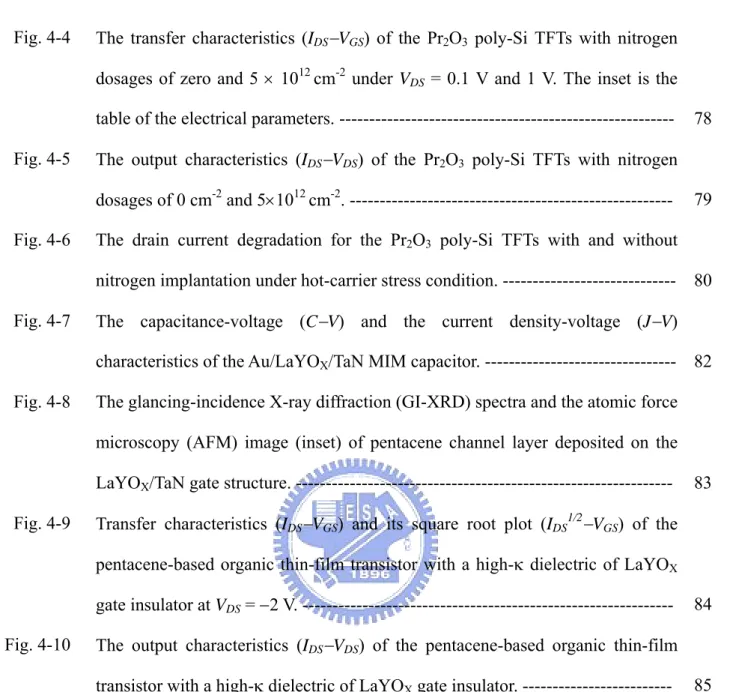
(22) Metal Pad. Channel Passivation. Organic Channel Gate Insulator. Metal Pad. Injection Organic Materials Interface Modification. High-κ Gate Metal Glass Substrate Fig. 1-4. The methods to improve characteristics of organic thin-film transistor (OTFT).. Fig. 1-5. Organic materials used as active channel layers for organic thin-film transistors (OTFTs) [21]. -8-.
(23) CHAPTER 2 GENERAL BACKGROUND AND LITERATURES REVIEW In this chapter, we first give a brief introduction on the active-matrix liquid crystal display (AMLCD) where the thin-film transistors (TFTs) as the switching devices or the controlled devices are fabricated. Second, a history for manufacturing TFT devices is described from the first TFT device to the low-temperature polycrystalline silicon (LTPS) TFT and the organic TFT (OTFT). The section 2.3 presents a review on some kinds of organic semiconductor materials used for OTFT and their conduction mechanisms. In the subsequent section 2.4, the principle of solid-phase crystallization (SPC) method as well as several modified SPC methods to improve device performance are described and explained here. Section 2.5 gives a brief comparison of various high-κ materials, especially on the properties of. the. lanthanum. series. materials,. such. as. praseodymium. oxide. (Pr2O3). and. lanthanum-yttrium oxide (LaYOX). Moreover, the advantages for incorporating these high-κ dielectrics in TFTs and in OTFTs are also illustrated in this section. And then, the retrospective reviews on LTPS TFT and OTFT with high-κ gate dielectrics are shown in section 2.6. Finally, the current equations of these TFT devices used in the following chapters are derived in section 2.7.. 2.1. ACTIVE-MATRIX LIQUID CRYSTAL DISPLAY TECHNOLOGY Thin-film transistors (TFTs) are commonly utilized as pixel-switching elements in. active-matrix liquid crystal display (AMLCD). Fig. 2-1 shows the cross-sectional view of the unit pixel in an AMLCD [26]. Basically, the unit pixel in AMLCD consists of three main parts, a thin-film transistor (TFT), a liquid crystal (LC), and two polarizers on outer top and bottom -9-.
(24) glasses. The liquid crystal (LC), a group of rod-shaped polymer molecules, is confined between two glass plates separated by a spacer, and it would be forced by the orientation alignment layers either into 90° or 270°. The outer surfaces of two glass plates are coated with linear polarizers whose polar orientations are mutually perpendicular. When the unpolarized light travels through this AMLCD system, it is linearly polarized by the first polarizer, and subsequently the polarization plane of light could be rotated by the twisted LC molecules. This rotation enables the light to pass the second polarizer, which is perpendicular to the first polarizer. Hence, the AMLCD system is transparent in non-activated state. Besides, the inner surface of glass substrate contains patterned pixel electrodes made by a transparent conductor of indium-tin oxide (ITO). When an output voltage of switching TFT device is applied on the pixel electrode, the LC molecules would be aligned parallel to the electric field and perpendicular to the surface of the glass substrate. Therefore, the light polarization is not rotated anymore, and the crossed-polarization filters would result in blocking light, appeared to black in this unit pixel. Grey levels could be obtained with the partial alignment of liquid crystal (LC) molecules by applying various voltage levels on the pixel electrode. The red, green, and blue color filters are implemented on the front glass for individual pixels of full-color display. The first matrix concept on liquid crystal display (LCD) was proposed by Lechner et al. [27] in 1971. This equivalent circuitry of active matrix concept is drawn in Fig. 2-2. Each crossing region surrounded by row line and column line is located a thin-film transistor (TFT) and a pixel capacitor (Cp). The pixel capacitor represents both the capacitances of liquid crystal and additional storage capacitor. The data driver and the scan driver, the peripheral circuitry generally fabricated by complementary-metal-oxide-semiconductor (CMOS) process, control the gate voltage and the drain voltage of each thin-film transistor, respectively. The scan driver controls the gate addressing, and its alternate sweeping depends on how much frame rate we need. The data driver inputs the information of video signals by various voltage - 10 -.
(25) levels stored on the pixel capacitor (Cp). Various amounts of charges in the pixel capacitor related to the polarization of liquid crystal (LC) result in the various grey levels we see on the active-matrix liquid crystal display (AMLCD).. 2.2. HISTORY OF THIN-FILM TRANSISTORS The first n-type thin-film transistor (TFT) was fabricated by P. K. Weimer at RCA. laboratory in 1962 [28]. He used the thin film of microcrystalline cadmium sulfide (CdS), the insulator of silicon monoxide, and the electrodes of autumn (Au) to form CdS TFT with a top-gate staggered structure on glass substrate, as shown in Fig. 2-3. All of these materials in this device were deposited by utilizing electron-beam evaporation through shadow masks. In 1964, P. K. Weimer also reported a p-type TFT with a tellurium (Te) active channel with the same structure [29]. Although the active channel of polycrystalline CdS or Te has a high mobility characteristic, the other electrical properties are influenced by grain size, stoichiometry, high interface states, and even sensitive to ambient gas. Therefore, in 1979, LeComber et al., first introduced the radio-frequency (RF) sputtered amorphous silicon (α-Si) as the active channel material of TFT device [30], as shown in Fig. 2-4. With the process progressing, in 1986, Funada et al., of Sharp fabricated the TFT with a tri-layer inverted-staggered structure contained a back-channel insulating layer, an etch-stopper layer, an active layer, and a source/drain contact layer which those layers are all deposited by a plasma-enhanced chemical vapor deposition (PECVD) system [31]. With this tri-layer inverted-staggered structure, it is easy not only to make the good contact with the back-channel approach but also to control the OFF-state current with the shading-light bottom-gate electrode. It becomes the standard structure of amorphous silicon (α-Si) TFT in modern active-matrix liquid crystal display (AMLCD) technology [32], as shown in Fig. 2-5. In following years, based on α-Si technology, many kinds of electronic products equipped. - 11 -.
(26) with AMLCD panels are commercialized, such as LCD monitors, notebooks, and the state of the art: super large size TFT-LCD TV of 108 inches fabricated by Sharp with its 7-th generation production line in 2007. Because the mobility of amorphous silicon (α-Si) TFT was too low with an approximate value of 0.2 to 1 cm2/V-s, in 1980, Funada et al., of IBM reported the first high-temperature polycrystalline silicon (poly-Si) TFT with a high mobility of 50 cm2/V-s fabricated on quartz substrate [33], but it could not be fabricated on glass substrates due to the temperature limitation. Afterwards, many researches [34], [35] focused on how to use a low-temperature process to fabricate top-gate poly-Si TFTs on glass substrate, as shown in Fig. 2-6. In 1991, Little et al., of Seiko-Epson first developed a low-temperature polycrystalline silicon (LTPS) TFT on glass substrate by using solid-phase crystallization at 600 °C, whose mobility was close to that on quartz substrate [36]. Further, various crystallization technologies were developed to improve the device performance, for examples, metal induced crystallization [37], [38] and laser crystallization [39], [40]. With these advanced crystallization technologies, the LTPS TFT device with a high mobility was not only used as the switching element with a larger aspect ratio (AR) in unit pixel, but also made as the device in periphery driving circuit and in control circuit around the panel, as shown in Fig. 2-2. Currently, by combining the laser crystallization technology, the LTPS TFTs have been used in small-to-mid size panel products, such as digital camera or cellular phone, for high delicate pixel, high definition, and portable and low-power electronics applications. In previous section, pursing high performance of TFT device drives new technologies used in FPD field. However, not all electronics require high performance. Some devices, for examples, detectors, electrical papers, or electrical clothes, only have to cover large area, no need to high definition, and must be produced with extremely low cost or disposable. Some devices have to integrate with personal information on a plastic substrate, such as smart cards or identification tags. For these special applications, large area coverage, mechanical - 12 -.
(27) robustness, and cheap and low-temperature production, are the most important consideration rather than intrinsic performance. Therefore, the cheaper organic semiconductors with similar mobility to the amorphous silicon (α-Si) have been attracted much attention recently. Various organic semiconductors have been studied since the early 1950s [41], but their characteristics were poor and low reproducible. The electrical conduction of the polymer-based polyacetylene was first reported by Chiang et al. in 1977 [42]. A few years later, Ebisawa et al., fabricated the first polymer-based transistor with a polyacetylene (CHx) channel in 1983 [43]. Owing to the thermal and mechanical fragility of the organic materials, the inverted-staggered structure and the inverted coplanar structure are most frequently used structures in the organic-based TFTs field, as shown in Figs. 2-7(a) and 2-7(b), respectively [44]. Nowadays, all organic semiconductors are conjugated organic materials with single and double carbon bonds alternated along whole molecule backbone. Based on the molecular weight, the organic semiconductors roughly have two classifications as (1) conjugated polymers and (2) small molecules or short conjugated oligomers [45]. Among these organic semiconductors, the oligomers pentacene (C22H14) has the highest mobility. Recently, the saturation mobility of the pentacene-based thin-film transistor with a 400-nm thermal gate oxide on heavily doped silicon substrate was progressive to 1 cm2/V-s [46], [47], whose characteristics are shown in Fig. 2-8. However, such device needs high operational voltage so that it could not be used for low-power circuit applications.. 2.3. ORGANIC SEMICONDUCTOR MATERIALS In conjugated organic materials, single and double bonds alternate along whole molecule. backbone. It means that all π orbitals of the carbon atoms participates to either a double bond or a single bond from a sort of continuous π bond delocalized along the whole molecule. The hybridization of the π orbital results in splitting of the energy levels and forming a sort of the. - 13 -.
(28) Highest-Occupied-Molecular-Orbit (HOMO) analogous to the valence band of conventional inorganic semiconductor. Besides, the anti-bonging π* orbitals, with their higher energy, constitute the Lowest-Unoccupied-Molecular-Orbit (LUMO) like the conduction band of inorganic semiconductor. The energy band diagrams of oligo-thiophenes and poly-thiophenes are also the function of the number of conjugated units [48], as shown in Fig. 2-9. On the contrary, the transport from one molecule to another is much more difficult due to a small energetic coupling between molecules held by a weak Van der Waals force about 10 kcal/mol [49]. Generally, the inter-molecular transport could not be described with the conventional band theory, but it could be described as the phonon assisted carrier hopping between the localized states of organic molecules. Accordingly, unlike the case of the phonon scattering for conventional inorganic semiconductor [45], the mobility (μm) of these organic molecules increases with temperature following an exponential form as ⎡ ⎛ T0 ⎞1/ α ⎤ μm = μm,0 exp ⎢ − ⎜ ⎟ ⎥ ⎣⎢ ⎝ T ⎠ ⎦⎥. (2-1). , where α is an integer ranging from 1 to 4, T is temperature, and T0 and μm,0 are fitting constant. However, concerning the higher ordered organic materials, the explanation for inter-molecular conduction by hopping process may face some controversy [45]. Depending on the arrangement of molecules and the nature of majority charge carriers, organic semiconductors could be either p-type or n-type materials. Several commonly used organic and polymer semiconductor materials with reliable performance characteristics for thin-film device are shown in Fig. 2-10 [21]. Pentacene (C22H14) and regioregular poly(3-hexylthiophene) (P3HT) have been extensively researched and commonly used for p-type material in most organic TFT devices. However, n-type materials are also required for special applications, such as organic light emitting diodes (OLED) or organic-based complementary-metal-oxide-semiconductor. (O-CMOS),. -dicyanoperylene-3,4:9,10-bis(dicarboximide) - 14 -. including. (PDI-8CN2),. and. N,N’-bis(n-octyl)hexadecafluoro-.
(29) -phthalocyanine (F16CuPc). In our study, pentacene, as a member of oligomers, consists of five aligned and condensed benzene rings is used to demonstrate our organic TFT with high-κ dielectric.. 2.4. SOLID-PHASE CRYSTALLIZATION TECHNOLOGY As-deposited polycrystalline silicon (poly-Si) film as an active channel layer generally. exhibits small grain size resulting in inferior characteristics of low-temperature polycrystalline silicon (LTPS) thin-film transistor (TFT). In poly-Si film, most of defects in grain boundaries would act as scattering centers or midgap trap states to degrade carrier transport properties and to increase off-state leakage current in LTPS TFT [50]. Consequently, a low-cost solid-phase crystallization (SPC) process is developed to re-crystallize poly-Si film from amorphous silicon (α-Si) film and it could obtain larger grain size to minimize grain boundaries in active channel layer corresponding to the improvement of ploy-Si quality [51]. A small amount of scattering centers and trap states in active channel layer result in a higher carrier mobility in LTPS TFT. In our work, therefore, we use SPC method to demonstrate the LTPS high-κ TFT with various nitrogen dosages. Given sufficient energy to overcome initial energy barrier, amorphous silicon (α-Si), a thermodynamically metastable phase, has a driving force to transform toward polycrystalline phase. After the α-Si film is deposited, the traditional SPC process spends several hours (> 20hrs) for completely converting the α-Si film to the poly-Si film at a low temperature of 600 °C. The grains are generally elliptical in shape due to preferential growth in <112> direction, and dendritic due to the formation of twin along (111) boundaries, as shown in Fig. 2-11 [52]. Besides, as the cross-sectional view of TEM in Fig. 2-12 [53], the traditional SPC process is an interface-nucleation scheme generating lots of nucleation sites at the amorphous silicon/underlayer (α-Si/SiO2) interface as a function of annealing time. It also results in many. - 15 -.
(30) grain boundaries in re-crystallized poly-Si film, in spite of less than those in amorphous silicon (α-Si) film [54]. In order to improve the microstructure of poly-Si film, the modified solid-phase crystallization (SPC) methods with surface-nucleation scheme are proposed by introducing oxygen dopants at the amorphous silicon/buffer oxide layer (α-Si/SiO2) interface to suppress grain nucleation starting at this interface [55], [56]. It initially nucleates at another preferable nucleation site on the top free surface of α-Si film to gain a larger grain size of poly-Si film. In order to further decrease the trap states in grain boundaries, the hydrogen plasma [7] or the ammonia plasma [8] passivation is treated after the LTPS TFT is finished. However, the hydrogenated poly-Si TFTs suffer from a serious instability issue due to the easily broken of weak Si-H bonds under electrical stress [57]. To find stronger and more stable bonds, such as S-F bond or Si-N bond, to replace the Si-H bonds in passivation process, the fluorine implantation [58], the carbon tetrafluoride (CF4) plasma treatment [59], and the nitrous oxide (N2O) plasma treatment [60] are processed on the active channel layer after the SPC process is completed. Furthermore, the low-temperature SPC activation with implanted fluorine ions is also proposed [61] to improve the electrical characteristics and the reliability of LTPS TFTs. According to these previous reports, we could conclude that the stronger bonds formed in the poly-Si film and at poly-Si/gate insulator could significantly improve performance and reliability of device. Therefore, in our study, we propose the LTPS TFT with nitrogen incorporation during SPC process to form the stronger Si-N bonds and to passivate the trap states in poly-Si grains and in grain boundaries. We expect such device has better electrical stress immunity.. - 16 -.
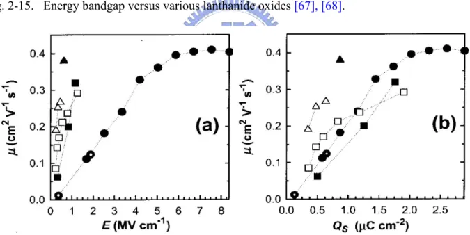
(31) 2.5. THE PROPERTIES OF HIGH-κ MATERIALS Today, searching potentially alternative high-κ materials as gate insulators has attracted. much attention in complementary-metal-oxide-semiconductor (CMOS) technology. Through the publications of well-known international journals and conferences, as shown in Fig. 2-13, the research trend gradually changes from binary oxides to ternary oxides as well as from hafnium-based dielectrics to lanthanide oxides. Besides, the new dielectric must satisfy some criteria, including large energy bandgap (EG) and high dielectric constant (κ) value. The capacitor fabricated by using dielectric material with a large energy bandgap and a high dielectric constant value could obtain a low leakage current and a large capacitance density, respectively. However, the dielectric constant and the bandgap of high-κ dielectric materials are usually trade-off. Fig. 2-14 shows the energy bandgap of several candidate oxides for gate dielectric as a function of the dielectric constant [62], [63]. The most promising dielectric in terms of the figure of merit (FOM) is given by the product of the energy bandgap and the dielectric constant. Therefore, we choose the materials with energy the bandgap larger than 5 eV and the dielectric constant larger than 20 as gate dielectrics, as shown in the oblique-line region of Fig. 2-14, including hafnium-based oxide, zirconium-based oxide, and lanthanide-based oxide. Lanthanide oxides are possible candidates of gate dielectrics to replace the hafnium-based oxide in the next generation [64]. Lanthanide oxides have good thermal stability in contacting with silicon [65], and the most of their dielectric constant values are large enough. For example, the lanthanum oxide (La2O3) as a gate dielectric has been reported a high dielectric constant value up to 27 [66]. The energy bandgap (EG) and the conduction band offset relative to silicon (ΔECB) of the lanthanide oxides also meet the requirements for gate dielectrics, being EG ~ 4 to 6 eV and ΔECB > 2 eV, respectively [67], [68]. Fig. 2-15. - 17 -.
(32) shows the energy bandgaps of various lanthanide oxides. Except for the EG of the cerium oxide (CeO2) smaller than 2.5 eV, the other lanthanide oxides have a EG larger than 4 eV [67], [68]. Therefore, in this study, we choose praseodymium oxide (Pr2O3) and lanthanum-yttrium oxide (LaYOX) as our gate dielectrics for integrating into LTPS TFT and organic TFT, respectively. The reasons why we choose these two lanthanide oxides as the gate insulators are shown in next subsection.. 2.5-1 Characteristics of Praseodymium Oxide Praseodymium oxide, a rare earth metal oxide, has been used for microelectronic applications so far. The praseodymium oxide have three various crystallographic structures, which PO2 exhibits the cubic calcium fluoride structure with C1-type, and Pr2O3 crystallizes in the manganese oxide structures with D 53 type and D 52 type [69], [70]. The D 53 type structure is based on the calcium fluoride structure where a quarter of the oxygen atoms are removed from specific lattice sites. It has been reported that the Pr2O3 with hexagonal lanthanum oxide structure of D 52 type is suitable for epitaxy on Si (100) substrate only [69]. The melting point and the boiling point of praseodymium oxide (Pr2O3) are 2183 °C and 3760 °C, respectively [70]. Praseodymium oxide (Pr2O3) as the gate dielectric on Si substrate has a dielectric constant up to 31, deposited by molecular beam epitaxy (MBE) equipped with electron-beam evaporator [71]. As to the deposition of praseodymium oxide (Pr2O3) film, the studies on pulsed-laser deposition (PLD) method [72], [73] and metallorganic chemical vapor deposition (MOCVD) method [74] are also reported. The symmetrical valance and conduction band offsets relative to silicon (ΔEVB and ΔECB) of praseodymium oxide measured by X-ray photoelectric spectroscopy (XPS) valence band spectrum and Fowler-Nordheim plot are all larger than 1.2 eV, respectively [75]. Due to the middle bandgap of 4.0 eV and the large formation energy of −12900 kJ/mole [70], the praseodymium oxide (Pr2O3) should be more stable and popular for its application on Si substrate. Particularly, the praseodymium oxide - 18 -.
(33) (Pr2O3) film exhibits a leakage current densities 104 times lower than the hafnium oxide (HfO2) film and the zirconium oxide (ZrO2) film at the same equivalent oxide thickness (EOT) of 1.4 nm [76]. Moreover, Osten et al., also reported that the praseodymium oxide film is compatible with conventional COMS processes, and demonstrated that it is no need to re-engineer the manufacturing procedures [76].. 2.5-2 Characteristics of Lanthanum-Yttrium Oxide In 2001, W. Zhu et al., reported that incorporating some aluminum atoms into hafnium oxide (HfO2) film (about 30 %) could increase the crystallization temperature up to 1000 °C, and it also could decrease the gate leakage current due to the increase of thermal stability on Si substrate [77]. Due to the smaller dielectric constant value of aluminum-doped hafnium oxide (HfAlOX) (around 15), the lanthanum-doped hafnium oxide (HfLaOX) was proposed by Y. Yamamoto et al., with a high dielectric constant value around 25 [78]. The HfLaOX film has a wide bandgap around 5.5 eV and a good thermal stability with amorphous phase to 1000 °C so that its leakage current is very small. Even though the lanthanum oxide (La2O3) film is easy absorbent to become lanthanum hydroxide to degrade its dielectric constant value, the lanthanum-doped hafnium oxide film could solve this moisture absorption problem. Following, K. Kita et al., also reported on the yttrium-doped hafnium oxide (HfYOX) film (only need about 4 % yttrium) [79], which not only increases the thermal stability of hafnium oxide (HfO2) but also increases the dielectric constant by the structural phase transformation from monoclinic phase to cubic phase. The atom induced a smaller molar volume (Vm) or with a large polarizability (αm) could be chosen for doping source into high-κ dielectric [79]. The yttrium (Y) atom just conforms to these two criteria [79]. Besides, yttrium oxide (Y2O3) is also a high-κ dielectric material with a good thermal stability on silicon. Therefore, the high-κ lanthanum-yttrium oxide (LaYOX) film is proposed to solve the moisture absorption problem of lanthanum oxide and to increase the dielectric constant value to 29 with 40-to-60 % yttrium - 19 -.
(34) doped concentration [80]. This LaYOX film is deposited by radio-frequency (RF) co-sputtering of L2O3 and Y2O3 targets. The bandgap of LaYOX film with 50 % yttrium doping is also larger than 5.5 eV, and the leakage current and the hysteresis are lower than those of other reports under the same equivalent oxide thickness (EOT) [81].. 2.6. REVIEW ON HIGH-κ MATERIALS USED IN THIN-FILM TRANSISTORS In CMOS technology, for matching scaling rule to improve device performance,. especially on driving capability, the gate capacitance density (Cins) is continuously enlarged by using various high-κ materials with high dielectric constant values. On the other hand, in academic studies, the solid-phase crystallization (SPC) poly-Si TFT device also gradually incorporates the high-κ materials process to gain its benefits on device performance. The equivalent oxide thickness (EOT) of high-κ gate insulator could be thinner than that of the traditional tetraethoxylsilane (TEOS) gate insulator under the same physical thickness. Due to the same reason for using high-κ materials in CMOS technology, the high-κ poly-Si TFT also could increase the gate capacitance density to induce more inversion charge carriers in channel region. Therefore, the poly-Si TFT with high-κ dielectric could improve its gate controllability due to the driving capability enhancement. Several high-κ materials, including ONO stack oxide [82], nitrous oxide (N2O) [83], tantalum pentoxide (Ta2O5) [84], aluminum oxide (Al2O3) [85], lanthanum-aluminum oxide (LaAlO3) [86], and hafnium oxide (HfO2) [16], are proposed to replace the conventional TEOS oxide served as gate insulators for the poly-Si TFTs. The comparison on electrical characteristics of LTPS poly-Si TFTs with various gate insulators are summarized in Table 2-1. Unfortunately, implementing ONO stack oxide, nitrous oxide (N2O), and aluminum oxide (Al2O3) in LTPS TFTs could not effectively improve the device performance due to their low dielectric constant values. The tantalum - 20 -.
(35) pentoxide (Ta2O5) with a narrow energy bandgap, especially on its smaller conduction bandgap offset relative to silicon (ΔECB), is not suitable for n-type LTPS TFTs application due to the gate leakage current issue. By the way, in Table 2-1, the LTPS TFT with hafnium oxide (HfO2) gate dielectric has the smallest threshold voltage (VTH) of 0.3 V. The reason is that its channel width is 100 nm approximate to the thickness of active channel of 50 nm so that its operation mode is like Fin-FET device with well gate controllability. Besides, the 30-min ammonia (NH3) plasma treatment is also contributed to passivate the trap states in the grain boundaries and interface of this LTPS TFT with a hafnium oxide (HfO2) gate dielectric. Furthermore, OTFT with a low mobility and a high operation voltage, compared to LTPS TFT, is more necessary to introduce the high-κ dielectric process to improve the device performance. The mobility of pentacene-based OTFT increases linearly with the increase of electric field (E) and charge density in channel layer (QS), but eventually saturates, as shown in Fig. 2-16 [25]. QS is a function of the accumulated carriers concentration in channel layer. Except for thermal oxide (SiO2), gate dielectrics with high-κ materials could induce more charge density in channel layer (QS) under the same electric field (gate and drain voltages) corresponding to the channel mobility (μ). Table 2-2 shows the comparison on electrical characteristics of pentacene-based OTFTs with various gate dielectrics, including thermal oxide (SiO2) [25], barium zirconate titanate (BZT) [25], gadolinium oxide (Gd2O3) [87], tantalum pentoxide (Ta2O5) [88], lanthanum-aluminum oxide (LaAlO3) [89], titanium oxide (TiO2) [90], manganese-doped barium strontium titanate (Mn-BST) [91], and titanium-silicon oxide (TiSiO) [92]. We can see that the mobility of pentacene-based OTFTs without interface modification from hydrophilic to hydrophobic [22]-[24] is within 0.1 to 0.4 cm2/V-s. When the gate capacitance density (Cins) is increased, the operational voltage and the threshold voltage (VTH) could be decreased, particularly on the highest Cins fabricated by titanium oxide (TiO2) [90]. By the way, the pentacene-based OTFTs using lanthanum-aluminum oxide (LaAlO3) has the best mobility. The reason is that introducing lanthanum (La3+) with ionic - 21 -.
(36) bond nature and as the same valence as that of aluminum (Al3+) reduce the dangling bonds caused by Al3+ so that improve the mobility and hysteresis [89]. Therefore, in our work, we use the same kind of lanthanum-yttrium oxide (LaYOX) as the gate insulator processed in pentance-based OTFT.. 2.7. CURRENT EQUATIONS OF THIN-FILM TRANSISTORS. 2.7-1 Drain Current Equations in Linear and Saturation Regions In this section, we formulate a general drain current for thin-film transistor by using gradual channel approximation (GCA) model [93], which the variation of the electrical field along the channel is much less than that along the corresponding variation perpendicular to channel. Hence, the inversion charges density ( Qinv ) could be simplified to the 1-D form of Possion’s equation, as shown in Fig. 2-17 [93]. The current-voltage characteristic of the thin-film transistor could be calculated by estimating the elemental resistance dR and the elemental segment dy of the conducting channel given by dV = I DS dR = I DS. W μ EF. dy | Qinv ( y ) |. (2-2). , where W is the channel width and μ EF is the field-effect mobility. And then, integrating Eq. (2-2) from source (V=0 at y=0) to drain (V=VDS at y=L), the drain current could be expressed as L. ∫I 0. DS. dy = μ FEW. VDS. ∫ 0. Qinv dV Î I DS. W = μ FE L. VDS. ∫. Qinv dV .. (2-3). 0. Following, we use the charge-sheet approximation model [94], which assumes that the inversion charges ( Qinv ) are located at the silicon surface as a sheet of charges with no potential dropping or band bending across the inversion layer, to derive drain current as Qinv = QS − Qdep = −Cins (VGS − V fb − 2ψ B − V ) + 2ε Si qN B ( 2ψ B + V ) - 22 -. (2-4).
(37) , where QS is the total surface charge density, Qdep is the depletion charge density, V fb is the flat band voltage, the surface potential ψ S is pinned at ψ S = 2ψ B + V ( y ) , Cins is the gate capacitance density of insulator layer, ε Si is the dielectric constant of silicon, and N B is the effective channel dpoant in active channel of the thin-film transistor. Substituting Eq. (2-4) into Eq. (2-3) and carrying out the integration, the drain current ( I DS ) could be presented by I DS. W = μ FE L. VDS. ∫. Qinv dV = μ FE Cins. 0. W⎧ m 2⎫ ⎨(VGS − VTH ) VDS − VDS ⎬ 2 L⎩ ⎭. (2-5). , where the body-effect coefficient m and the threshold voltage VTH are m = 1+. ε Si qN B / 4ψ B Cins. and VTH = V fb + 2ψ B +. 4ε Si qN Bψ B Cins. , respectively.. (2-6). When the device works in saturation region, the I DS is independent on VDS , which means. dI DS ⎛ V −V = (VGS − VTH ) − mVDS = 0 Î VDS = VDS , sat = ⎜ GS TH m dVDS ⎝. ⎞ ⎟. ⎠. (2-7). Substituting Eq. (2-7) into Eq. (2-5), the saturation current I DS , sat could be written as. I DS , sat. W (VGS − VTH , sat ) = μ FE , sat Cins 2m L. 2. (2-8). In m = 1 case, the Eq. (2-5) and Eq. (2-8) could be simplified by I DS ,lin = μ FE ,lin Cins. W⎧ 1 2⎫ ⎨(VGS − VTH ,lin ) VDS − VDS ⎬ L⎩ 2 ⎭. for linear operation. (2-9). and. I DS , sat =. 2 1 W μ FE , sat Cins (VGS − VTH , sat ) 2 L. for saturation operation, respectively.. (2-10). 2.7-2 Drain Current Equations in Subthreshold Region To derive the subthreshold current, we start at solving Poisson’s equation in the surface region of semiconductor, whose detail band diagram and potential of p-type silicon are summarized in Fig. 2-18 [93]. The Poisson’s equation in this band diagram could be - 23 -.
(38) re-written as ⎛ −qψ dξ d 2ψ q ⎡ ⎛ = − Si = − ⎢ N B ⎜⎜ exp ⎜ 2 ε Si ⎣⎢ ⎝ d x dx ⎝ k BT. ⎞ ⎞ ni 2 ⎛ ⎛ qψ ⎜⎜ exp ⎜ ⎟ − 1⎟⎟ − ⎠ ⎠ NB ⎝ ⎝ k BT. ⎞ ⎞⎤ ⎟ − 1⎟⎟ ⎥ ⎠ ⎠ ⎦⎥. (2-11). , where ψ is the potential in silicon, ξ Si is the electric field in silicon, and k B is the Boltzmann constant. At x = 0 , let ψ = ψ S (surface potential). Based on the Gauss’s law, the total charge density ( QS ) is QS = Qacc + Qdep + Qinv = −ε Siξ Si = ε Si ∫. d 2ψ ⎛ dψ ⎞ dx ⎟ . ⎜ d 2 x ⎝ dx ⎠. (2-12). Substitute Eq. (2-11) into Eq. (2-12) and arrange the QS as 1/ 2. 2 ⎧⎪⎛ ⎛ qψ s ⎞ ⎛ qψ s ⎞ ⎞ ⎛ ni ⎞ ⎛ ⎛ qψ s ⎞ ⎛ qψ s ⎞ ⎞ ⎫⎪ QS = 2ε Si k BTN B ⎨⎜⎜ exp ⎜ − ⎟−⎜− ⎟ − 1⎟⎟ + ⎜ ⎟ ⎜⎜ exp ⎜ ⎟−⎜ ⎟ − 1⎟⎟ ⎬ . ⎝ k B T ⎠ ⎝ k BT ⎠ ⎠ ⎝ N B ⎠ ⎝ ⎝ k BT ⎠ ⎝ k BT ⎠ ⎠ ⎪⎭ ⎪⎩⎝. (2-13). In substhreshold operation, we only consider the inversion charge density ( Qinv ) in channel region, and the last significant terms of Eq. (2-13) could be re-written as ⎛ q (ψ S − V ) ⎞ ε qN k T ⎛ n ⎞ Qinv = Si B B ⎜ i ⎟ exp ⎜ ⎟ 2ψ S q ⎝ NB ⎠ ⎝ k BT ⎠ 2. (2-14). , where the (ψ S − V ) term is considered as the influence of drain voltage on active channel. Substituting Qinv of Eq. (2-14) into Eq. (2-3), and carrying out the integration, the drain current in the subthreshold region ( I DS , SUB ) could be presented by. I DS , SUB. W = μ FE L. VDS. ∫ 0. W Qinv dV = μ FE Cins L. 2. 2. ⎛ qψ S qε Si N B ⎛ k BT ⎞ ⎛ ni ⎞ ⎟ exp ⎜ ⎜ ⎟ ⎜ 2ψ S ⎝ q ⎠ ⎝ N B ⎠ ⎝ k BT. ⎞ ⎟. ⎠. (2-15). 2.7-3 Drain Current Equations of Organic Thin-Film Transistors Most organic thin-film transistors operate in the accumulation region, where the gate voltage is polarized positively (negatively) versus the n-type (p-type) substrate. Because organic thin-film transistor operates in accumulation region, we only take account in the - 24 -.
(39) accumulation charges density ( Qacc ) and the free carrier density ( Q0 ) in organic channel layer, where Q0 = qn0 d s and QS = Cins ⎡⎣VGS − V fb − V ( y ) ⎤⎦ ~ Qacc .. (2-16). In Eq. (2-16), n0 is the density of free carriers at equilibrium, d s is the thickness of the semiconductor, Cins is the gate capacitance density, V fb is the flat band voltage, and V ( y ) is accounted as the drain influence. Because the organic thin-film transistor works in accumulation mode, QS ( y ) and Q0 , the total charges in channel, have identical sign neglecting the ohmic drop in channel. Hence, the drain current in linear region (in VDS < VGS ) could be obtained from gradual channel approximation (GCA) model dV = I DS ,lin dR = I DS ,lin. dy . W μ EF ,lin | QS ( y ) + Q0 |. (2-17). Substituting Eq. (2-16) and Eq. (2-17) into Eq. (2-3), we can obtain I DS ,lin = μ FE ,lin. ⎡ V 2⎤ W Cins ⎢(VGS − VTH ,lin ) VDS − DS ⎥ 2 ⎦ L ⎣. (2-18). , where VTH ,lin is the threshold voltage in linear region and could be written as. VTH ,lin = V fb +. qn0 d s . Cins. (2-19). However, when VDS > VGS , the accumulation layer near drain changes to a depletion layer, as shown. in. Fig.. 2-19. [95].. In. depletion. region,. there. is. no. free. carrier. at. semiconductor/insulator interface. Thus, the integrating term of free carriers Q0 in Eq. (2-16) should be modified as. Q0 = qn0 ⎡⎣ d s − W ( y ) ⎤⎦. (2-20). , where W ( y ) is the depletion width near the drain region. And, the depletion width could be solved by the voltage drop equation as. - 25 -.
(40) VGS − V fb − V ( y ) = VOX + VSemi. qN BW ( y ) qN BW 2 ( y ) = + ~ VGS − V ( y ) 2ε Semi Cins. (2-21). , where N B is the dopant concentration and ε Semi is the dielectric constant of the organic semiconductor. Then, the depletion width near drain W ( y ) could be solved as W ( y) =. ε Semi ⎡⎢ Cins ⎢ ⎣. 1+. 2Cins 2 ⎡⎣VGS − V ( y ) ⎤⎦ qN B. ⎤ − 1⎥ . ⎥ ⎦. (2-22). Hence, substituting Eq. (2-22) and Eq. (2-20) into Eq. (2-3), and the drain current in saturation region ( VDS > VGS ) could be expressed as I DS , sat. W = μ FE , sat Cins L = μ FE , sat. W Cins L. VGS. ∫ ⎡⎣V. GS. 0. VGS. ∫ ⎡⎣V. GS. 0. − VTH , sat. W − V ⎤⎦ dV +μ FE , sat qn0 L. W L. ∫. ⎡⎣ d s − W ( y ) ⎤⎦ dV. 0. − VTH , sat − V ⎤⎦ dV. W q 2 n0 N B + μ FE , sat L ε Semi. = μ FE , sat. Vdsat. dS. ∫ (d 0. s. ⎛ ε − W ) ⎜ W + Semi Cins ⎝. ⎞ ⎟ dW ⎠. ⎡ ⎛ VGS 2 ⎞ q 2 n0 N B d s 3 ⎛ CSemi ⎞ ⎤ C V V − ⎢ ins ⎜ ⎜1 + 3 ⎟⎥ . GS TH , sat ⎟ + 2 ε 6 C ⎝ ⎠ Semi ins ⎠ ⎦ ⎝ ⎣. (2-23). Because the organic thin-film transistor has a thin semiconductor layer, CSemi >> Cins , where CSemi is the depletion capacitance density of. ε Semi ds. . Assuming. N B = n0. yields. qN B d s = VTH , sat , and the Eq. (2-23) could be made as Cins I DS , sat =. =. ⎛ qN B d s ⎞ W 1 μ FE , sat Cins ⎜ VGS 2 − 2VGSVTH , sat + VTH , sat ⎟ 2 L Ci ⎠ ⎝ 2 1 W μ FE , sat Cins (VGS − VTH , sat ) . 2 L. (2-24). This formula is the saturation drain current of the organic thin-film transistor.. - 26 -.
(41) Common Electrode (ITO). Spacer Polarizer. Seal. Color-Filter Substrate. Color-Filter (Blue). Short. TFT. LC Alignment Layer. TFT-Array Substrate Polarizer Bonding PAD. Pixel Electrode (ITO). Storage Capacitor. Fig. 2-1. Cross-sectional view of a unit pixel in active-matrix liquid crystal display (AMLCD) [26].. Data Driver, (Video Signal) Scan Driver, (Gate Addressing). Ncol Vg m-1. TFT Vd. Cp m. Nrow. m+1 n-1. n. n+1. Fig. 2-2. The equivalent circuitry for the addressing matrix of an AMLCD [27].. - 27 -.
(42) Fig. 2-3. Schematic diagram of Weimer’s CdS TFT with top-gate staggered structure [28].. Fig. 2-4. Schematic diagram of LeComber’s amorphous silicon (α-Si) TFT structure and its transfer characteristics [30].. Fig. 2-5. Schematic cross section of an α-Si TFT with the “etch-stopper” layer and the in-situ tri-layer [32].. - 28 -.
(43) Fig. 2-6. Schematic cross section of a top-gate low-temperature polysilicon TFT with a storage capacitor [34].. S. Organic Semi.. Organic Semi.. D S. D. Insulator Gate. Insulator. Substrate. Substrate. (a). (b). Gate. Fig. 2-7. Schematic of the geometries frequently used in organic thin-film transistors with (a) inverted-staggered structure, and (b) inverted-coplanar structure [44].. Fig. 2-8. The output characteristic and the transfer characteristic of the pentacene-based organic thin-film transistor with a high saturation mobility of 0.62 cm2/V-s [46].. - 29 -.
(44) Energy Level (eV). 0 LUMO. Conduction Band. -2.5. Eg. -5. Valance Band. -7.5 HOMO -10. n~. 1. 2. 3. ∞. 4. Number of Conjugated Units Fig. 2-9. The energy levels of oligo-thiophenes and poly-thiophenes as a function of the number of conjugated units [48].. C6H13. (. Pentacene F F. F. F. N F. N. N. H17C3-N. N. F. F. N-C3H17. F O. O. N F. O. F. N. N. F. F F. n. NC O. Cu. N. ). P3HT. F. F. S. CN PDI-8CN2. F. F16CuPc Fig. 2-10. Commonly used high-performance organic and polymer semiconductor materials [21].. - 30 -.
(45) Fig. 2-11. Schematic of the re-crystallization mechanism for solid phase growth of amorphous silicon (α-Si) [52].. Fig. 2-12. TEM micrographs for amorphous silicon (α-Si) film as a function of annealing time, such as as-deposited, 1HR, 2HR, and 24HR [53]. - 31 -.
(46) Fig. 2-13. Summarized alternative high-κ gate dielectric materials reported in VLSI Symposium and IEDM from 1999 to 2005.. Energy Bandgap (eV). 10. SiO2. 9. Al2O3. 8. MgO. CaO. 7. ZrO2 HfO ZrSiO4 2 HfSiO4 Y2O3 La2O3 Si3N4. 6 5. Pr2O3. 4 3. Material Region. Ta2O5 0. 5. 10. 15. 20. 25. BaO 30. 35. Dielectric Constant Fig. 2-14. Energy bandgap versus dielectric constant plots for candidate gate insulators [62], [63]. - 32 -.
(47) 7. Energy Bandgap (eV). Lu2O3 6. La2O3. Sm2O3. Tm2O3. Gd2O3. 5. Pr2O3 4. Yb2O3 Nd2O3. 3 2. Ce2O3. Tb2O3. Eu2O3. Er2O3 Ho2O3. Dy2O3. 1. Lanthanide Oxides Fig. 2-15. Energy bandgap versus various lanthanide oxides [67], [68].. Fig. 2-16. Dependence of mobility (μ) on gate electric field (E). (b) Dependence of channel mobility (μ) on charge density (QS). Black or white sample correspond to channel mobility (μ) calculated from gate sweep or drain sweep, respectively. 500 nm SiO2 with gate sweeps (o); 120 nm SiO2 with gate sweeps (•); 82 nm BST with drain sweeps (♠); 90 nm BST with gate sweeps ( Δ ); 122 nm BZT with drain sweeps (); 128 nm BZT with gate sweeps (□) [25]. - 33 -.
(48) L X. IDS. W. Drain. Source y V(0)=0. dy. Semiconductor Insulator. V(L)=VDS. Gate VGS. VDS. Fig. 2-17. Schematic view of a thin-film transistor (TFT) under gate and drain biases [93].. Poission’s Equitation. dξ Si d 2ψ q ⎡⎣ p ( x ) − n ( x ) + N D + ( x ) − N A − ( x ) ⎤⎦ = − = − 2 ε Si d x dx 2 N D + ( x ) − N A− ( x ) = − N A +. ni ND. EC. qψ S > 0. VGS > 0. qψ ( x ) qψ B. Eg Ei Ef Ev. ⎛ q (ψ B − ψ ) ⎞ ⎛ − qψ ⎞ p ( x ) = ni exp ⎜⎜ ⎟⎟ = N A exp ⎜ ⎟ k BT ⎝ k BT ⎠ ⎝ ⎠. x. ⎛ q (ψ − ψ B ) ⎞ ni 2 ⎛ qψ ⎞ exp ⎜ n ( x ) = ni exp ⎜⎜ ⎟⎟ = ⎟ k BT ⎝ k BT ⎠ ⎝ ⎠ NA. Fig. 2-18. The energy bandgap diagram of the metal-insulator-semiconductor (MIS) structure under gate bias [93].. - 34 -.
(49) x Source. Accumulation V(x)=VGS. Drain. ds y. Insulator Gate VGS. Depletion. VDS. Fig. 2-19. Schematic view of an organic thin-film transistor (OTFT) working in accumulation region under high drain bias [95].. - 35 -.
(50) - 36 -. 5.14 12.4 1970 0.24. VTH (V). μFE (cm2/V-s). S.S. (mV/Dec.). ION/IOFF (106) 0.95. 642. 4.6. 4.75. 40/10. * Si0.85Ge00.15 TFT with Al2O3 dielectric. 50/10. ----. 40 nm. EOT. W/L (mm). 22 nm ONO [82]. 40 nm TEOS [60]. SPC TFT with Various Dielectrics. 0.3*. 440*. 47*. 3*. 200/3. 20 nm. 50 nm Al2O3 [85]. 6.3. 310. 40. 1.2. 100/4. 8.7 nm. 50 nm LaAlO3 [86]. 9.7 **. 280 **. 39 **. 0.3 **. 0.1/1. 7.3 nm. 27.7 nm HfO2 [16]. ** NH3 plasma passivation for 30 min. 1.72. 410. 26.8. 4.75. 50/10. ----. 21 nm N2O [83]. Table 2-1. Comparison on electrical characteristics of SPC poly-Si TFTs with various gate dielectrics, including TEOS oxide, ONO stack oxide, nitrous oxide (N2O), aluminum oxide (Al2O3), lanthanum-aluminum oxide (LaAlO3), and hafnium oxide (HfO2)..
數據
![Table 1-1. The roadmap of system integration trend of FPD provided by Sony Corporation [1]](https://thumb-ap.123doks.com/thumbv2/9libinfo/8227285.170788/20.892.113.793.765.1093/table-roadmap-integration-trend-fpd-provided-sony-corporation.webp)
![Fig. 2-1. Cross-sectional view of a unit pixel in active-matrix liquid crystal display (AMLCD) [26]](https://thumb-ap.123doks.com/thumbv2/9libinfo/8227285.170788/41.892.122.774.162.476/cross-sectional-active-matrix-liquid-crystal-display-amlcd.webp)
+7
![Fig. 2-7. Schematic of the geometries frequently used in organic thin-film transistors with (a) inverted-staggered structure, and (b) inverted-coplanar structure [44]](https://thumb-ap.123doks.com/thumbv2/9libinfo/8227285.170788/43.892.133.757.449.677/schematic-geometries-frequently-transistors-inverted-staggered-structure-structure.webp)
![Fig. 2-10. Commonly used high-performance organic and polymer semiconductor materials [21]](https://thumb-ap.123doks.com/thumbv2/9libinfo/8227285.170788/44.892.172.726.168.527/fig-commonly-used-performance-organic-polymer-semiconductor-materials.webp)
![Fig. 2-11. Schematic of the re-crystallization mechanism for solid phase growth of amorphous silicon (α-Si) [52]](https://thumb-ap.123doks.com/thumbv2/9libinfo/8227285.170788/45.892.184.700.117.495/schematic-crystallization-mechanism-solid-phase-growth-amorphous-silicon.webp)
![Fig. 2-14. Energy bandgap versus dielectric constant plots for candidate gate insulators [62], [63]](https://thumb-ap.123doks.com/thumbv2/9libinfo/8227285.170788/46.892.141.771.299.1042/energy-bandgap-versus-dielectric-constant-plots-candidate-insulators.webp)
![Fig. 2-18. The energy bandgap diagram of the metal-insulator-semiconductor (MIS) structure under gate bias [93]](https://thumb-ap.123doks.com/thumbv2/9libinfo/8227285.170788/48.892.163.728.545.1009/fig-energy-bandgap-diagram-metal-insulator-semiconductor-structure.webp)
相關文件
According to the Heisenberg uncertainty principle, if the observed region has size L, an estimate of an individual Fourier mode with wavevector q will be a weighted average of
雙極性接面電晶體(bipolar junction transistor, BJT) 場效電晶體(field effect transistor, FET).
The disabled person can thus utilize this apparatus to integrate variety of commercial pointing devices and to improve their controllability in computer operation.. The
• When the coherence bandwidth is low, but we need to use high data rate (high signal bandwidth). • Channel is unknown
• When the coherence bandwidth is low, but we need to use high data rate (high signal bandwidth). • Channel is unknown
In this thesis, we present a Threshold Jumping (TJ) and a Warp-Around Scan (WAS) techniques aim to coordinate simultaneous communications in high density RFID
―Low-Temperature Polycrystalline Silicon Thin Film Transistor Nonvolatile Memory Using Ni Nanocrystals as Charge-Trapping Centers Fabricated by Hydrogen Plasma
This thesis studies how to improve the alignment accuracy between LD and ball lens, in order to improve the coupling efficiency of a TOSA device.. We use
