國 立 交 通 大 學
電子工程學系 電子研究所
博 士 論 文
研究半導體和高介電絕緣體之介面以獲得
高性能之鍺及三五族金氧半場效電晶體
Improvement of High Dielectric Materials and
Semiconductor-Insulator Interfaces for Ge and III-V
High Performance MOSFETs
研 究 生 : 鄭 兆 欽
指導教授 : 張 俊 彥 院士
簡 昭 欣 教授
研究半導體和高介電絕緣體之介面以獲得
高性能之鍺及三五族金氧半場效電晶體
Improvement of High Dielectric Materials and
Semiconductor-Insulator Interfaces for Ge and III-V
High Performance MOSFETs
研 究 生: 鄭 兆 欽 Student:
Chao-Ching
Cheng
指導教授: 張 俊 彥 院士
Advisors:
Dr.
Chun-Yen
Chang
簡 昭 欣 教授
Dr. Chao-Hsin Chien
國 立 交 通 大 學
電子工程學系 電子研究所
博 士 論 文
A Dissertation
Submitted to the Institute of Electronics
College of Electrical Engineering and Computer Science
National Chiao Tung University
in Partial Fulfillment of the Requirements
for the Degree of
Doctor of Philosophy
in Electronics Engineering
June 2009
Hsinchu, Taiwan, Republic of China
研究半導體和高介電絕緣體之介面以獲得
高性能之鍺及三五族金氧半場效電晶體
研 究 生: 鄭 兆 欽
指導教授: 張 俊 彥 院士
簡 昭 欣 教授
國 立 交 通 大 學
電子工程學系 電子研究所
摘要
此 論 文 中 , 我 們 廣 泛 地 研 究 各 種 高 介 電 (high-k) 薄 膜 — 包 含 氮 氧 化 鉿 (HfOxNy)、三氧化二鋁(Al2O3)及三氧化二釓(Gd2O3)—在塊材鍺(Ge)及砷化鎵(GaAs)基板上的沉積及元件特性。首先,我們提出兩種表面鈍化方法,氨氣電漿 處理及超薄矽批覆,來改善氮氧化鉿濺鍍膜在純鍺基板上;而我們確實看到在經 過不管是表面氮化或矽覆蓋製程後,僅少量氧化鍺(GeOx)存在介電層接面、抑制 鍺擴散至上層氮氧化鉿以及較少的氧化層電荷捕獲。我們推測這些改善現象是由 於減少氧化鍺的揮發及提升高介電層/鍺接面熱穩定性的結果。 我們接續研究原子層沉積(atomic-layer-deposited)三氧化二鋁在純鍺基板上的 材料及電特性。發現提升沉積溫度確實改善三氧化二鋁本身的密度及當量化 (stoichiometry);但沉積溫度超過 200 度將造成三氧化二鋁介電層與氧化鍺接面層 的混合,也就是形成氧化鍺鋁中間層(GexAl1-xO intermediate layer),這將導致白金
/ 三 氧 化 二 鋁 / 鍺 (Pt/Al2O3/Ge) 電 容 元 件 出 現 較 大 漏 電 流 及 接 面 缺 陷 密 度
(interfacial state density)高達 1013 cm-2eV-1以上。另一方面,進一步採用氫氣氮氣
混合之熱退火(forming gas annealing)來改善低溫(100 度)三氧化二鋁沉積在鍺上
的特性,結果發現在靠近能帶中間(midgap)之接面缺陷密度可以下降至約 6×10¹¹
cm-2eV-1左右,連遲滯(hysteresis)現象也獲得改善。此外,我們結合電容元件實驗
與 MEDICI 模 擬 軟 體 , 進 一 步 證 實 具 有 高 本 質 載 子 濃 度 (intrinsic carrier concentration) 的 純 鍺 在 透 過 基 板 內 部 缺 陷 (bulk trap) 的 產 生 結 合 (generation/recombination)或擴散(diffusion)機制,是導致在高頻率下(>103 Hz)會
觀 察 到 低 頻 電 容 曲 線 及 無 電 壓 相 依 性 之 反 轉 電 導 (gate-independent inversion conductance)的主因。我們透過電導-電壓(conductance-voltage)特性評估出在低摻
雜濃度鍺基板內的缺陷密度約為(2-4)×1015 cm-3 左右。阿瑞尼士之基板電導圖
(Arrhenius-dependent substrate conductance)也指出在鍺基板內比起在矽基板內有
高達104倍的能量損耗(energy loss),的確反應出具有較快速的次要載子反應速度
(minority-carrier response rate)。
論文中,另一研究主題為改善濕式化學清潔(wet-chemical cleaning)及硫化氨
處理[(NH4)2S treatment]對於高介電層/砷化鎵之電特性影響。實驗證明,採用氨水
鹼性溶液(NH4OH alkaline solution)並搭配 80 度的硫化氨水溶液[(NH4)2S-H2O]可
有效地抑制砷化鎵原生氧化層(GaAs native oxides)及接面附近砷原子(elemental As)的形成,進而改善費米能階釘扎效應(Fermi level pinning effect)對電特性的影
響。所製造的三氧化二釓/砷化鎵(Gd2O3/GaAs)電容元件經過最佳化硫化處理後,
在電容等效厚度(capacitance-equivalent-thickness)約 20 埃及閘極電壓在平帶電壓 加 1 伏特[Vg = (VFB+1) V]條件下,可表現出漏電流僅約 1.5 × 10⁻⁵ A/cm2;已足以
匹配他人之前文獻使用超薄矽/鍺鈍化(ultrathin Si/Ge interfacial passivation)之二 氧化鉿/砷化鎵電容元件的優越電性表現。而原子層沉積之三氧化二鋁/砷化鎵
的頻率離散(frequency dispersion)、微縮的遲滯現象及較低的接面缺陷密度及漏電 流成果。且進一步將硫化氨的溶劑(solvent)從水換成丁醇(C4H9OH)將可看到更大 幅度的電特性改善,不僅明顯壓抑表面砷原子及氧化砷(AsOx)的量,也形成更多 穩定硫鍵結在砷化鎵基板上。另一方面,後續熱退火氣體環境的採用,氧氣及氮 氣,對原子層沉積三氧化二鋁/砷化鎵電容元件特性影響,已可透過了解背後熱化 學反應機制來理解。此外,我們也注意另一有趣現象,原子層沉積之三氧化二鋁 在砷化鎵基板上傾向於高溫(300 度)成長,剛好跟它在鍺基板上傾向於低溫(低於 200 度)成長是相反趨勢。 最後,我們成功地製作出搭配原子層沉積三氧化二鋁高介電層之反轉式 (inversion-mode)純鍺 P 型/N 型場效電晶體。純鍺 P 型電晶體(寬度/長度 = 100 μm/4 μm)呈現載子遷移率峰值(peak mobility)及電流開關比(on-off ratio)分別為 225 cm2V–1s–1及大於103;相對地,純鍺 N 型電晶體(寬度/長度 = 100 μm/9 μm)
的載子遷移率峰值及電流開關比分別低於100 cm2V–1s–1及103。而我們認為相對劣
等的 N 型電晶體特性主要跟具有較大的源極/汲極(source/drain)阻值、較嚴重的接
面缺陷散射效應以及較低的基板濃度有所關聯性。後續使用 300 度的氫氣氮氣混
合之熱退火不但可以提升驅動電流(on current)、降低能帶缺陷密度以及改善負偏 壓熱不穩定性(negative bias temperature instability)可靠度。但提升溫度至 400 度將 會極劇增加 N 型電晶體的關電流(off current),這是由於源極/汲極的磷摻雜發生嚴 重向外擴散所導致的結果。在此論文中,我們亦調查純鍺接面二極體特性及漏電
流路徑,我們得到純鍺P+N 及 N+P 接面二極體整流特性比分別可超過 103及104(電
壓範圍為±1 伏特),所對應的漏電流為接近 10-2 and 10-4 A/cm2。至於漏電流到底是 由表面周圍(surface perimeter)或接面面積(junction area)大小所主宰,發現熱製程 (摻雜活化或氫氣氮氣混合之熱退火)的使用乃是主要關鍵角色。另一方面,我們 也展示具有原子層沉積三氧化二鋁高介電層之空乏式(depletion-mode)砷化鎵 N 型 場效電晶體,在搭配硫化氨-丁醇表面處理後的轉換(transfer)及輸出(output)電特
性。在閘極電壓高於臨界電壓 4.8 伏特以及汲極電壓為 4 伏特(Vg–Vth = 4.8 V, Vd =
4 V)條件下,汲極電流(Id)約為250 mA/mm。但所萃取出來的電子遷移率峰值僅
Improvement of High Dielectric Materials and
Semiconductor-Insulator Interfaces for Ge and III-V
High Performance MOSFETs
Student: Chao-Ching Cheng
Advisors: Dr. Chun-Yen Chang
Dr. Chao-Hsin Chien
Department of Electronics Engineering and Institute of Electronics
National Chiao Tung University
Abstract
In this thesis we have extensively investigated the deposition of various high-k dielectric films—including HfOxNy, Al2O3, and Gd2O3—onto the bulk Ge and GaAs
substrates and the electrical characteristics of the devices with these developed high-k dielectric films. At first, two surface passivation methods, i.e., the NH3 plasma
pretreatment and the ultrathin Si capping, were employed to improve the quality of the sputtered HfOxNy films on the Ge substrates. Not only the severe incorporation of Ge
species into the overlying HfOxNy was eliminated, but also the smaller amount of GeOx
remained at the dielectric interface and the less oxide trapped charge were observed after undergoing surface nitridation or Si capping processes. These improvements can be attributed to the reduced GeOx volatilization and also enhanced thermal stability of
We subsequently studied the material and electrical properties of atomic-layer-deposited (ALD) Al2O3 thin films on the Ge substrates. It was found that
an increase in the deposition temperature did improve both the density and stoichiometry of the Al2O3 films; nevertheless, temperatures exceeding 200 °C caused
the intermixing of top Al2O3 and interfacial GeO2 layers, i.e., the formation of a
GexAl1–xO intermediate layer. It led to the consequence of an increasing gate leakage (Jg)
and a higher interface state density (Dit, >1013 cm–2eV–1) in the Pt/Al2O3/Ge capacitors.
On the other hand, for improving the quality of low-temperature (100 °C) Al2O3 films
on the Ge, the forming gas annealing (FGA) at 300 °C was conducted further; the value of the Dit close to midgap was evidently lowered to ca. 6 × 1011 cm–2eV–1 accompanying
with the reduced hysteresis width. In addition, we combined these device experiments with MEDICI simulations and thus validated that a high value of intrinsic carrier concentration (ni) in Ge, via the bulk-trap generation/recombination as well as the
diffusion from the bulk substrate, were responsible for the presence of low frequency C-V curves in the kHz regime and the gate-independent inversion conductance. The
density of the bulk trap was estimated to be ca. (2–4) × 1015 cm–3 in the low-doped Ge
in terms of their conductance-voltage (G-V) characteristics. The plot of the Arrhenius-dependent substrate conductance (Gsub) also indicated a larger energy loss
occurring in Ge than in Si by at least four orders of magnitude, reflecting the fast minority-carrier response rate.
We also, afterward, presented the study of the effects of alterant wet-chemical clean and (NH4)2S treatment on the electrical characteristics of high-k/GaAs devices.
Through analysis of the surface chemistry, it was evident that employing the NH4OH
alkaline solution and then (NH4)2S-H2O passivation at 80 °C effectively suppressed the
abating the “Fermi level (Ef) pinning” effect on the electrical performance. With
undergoing the optimized sulfidization processes, the fabricated Gd2O3/GaAs capacitors
exhibited the Jg of ca. 1.5 × 10⁻⁵ A/cm2 @ Vg = (VFB + 1) V with the
capacitance-equivalent-thickness of ca. 20Å, which is comparable to the earlier study of high-performance HfO2/GaAs system with an ultrathin Si/Ge interfacial passivation.
Also, the sulfidized ALD-Al2O3/GaAs capacitors can reveal the resultant higher oxide
capacitance, the smaller frequency dispersion, the decreased hysteresis width, the reduced Dit, and the smaller Jg, respectively. Further replacing the (NH4)2S solvent from
H2O to C4H9OH indicated a higher electrical improvement, in which an obvious
suppression of elemental As and AsOx surface species was found with an increasing
sulfur bonds on the GaAs substrates. On the other hand, the influences of post annealing ambient, O2 and N2, adopted in the Al2O3/GaAs capacitor were investigated and we
clarified the characteristic differences by identifying the underlying thermochemical mechanisms. In our studies, another interesting feature was noticed that the deposition of the ALD-Al2O3 films on GaAs favored to at the higher temperature, 300 °C, which is
opposite to the behavior that those on Ge favored to at low temperatures (<200 °C).
Finally, we have successively demonstrated the device characteristics of the inversion-mode Ge p- and n-MOS field-effect-transistors (FETs) with the ALD-Al2O3
gate dielectrics, respectively. The respective peak mobility and on/off ratio was ca. 225 cm2 V–1 s–1 and >103 for Ge p-FET (W/L = 100 μm/4 μm), while these values were less than 100 cm2 V–1 s–1 and ca. 103, respectively, for Ge n-FET (W/L = 100 μm/9 μm). The inferior n-FET device performance can be mainly correlated to the larger source/drain (S/D) contact resistance, the severe Dit scattering, and the lower level of substrate
doping. Subsequently performing FGA at 300 °C can enhance the driving on-current, decrease the Dit at the Al2O3–Ge interface, and improve the negative bias temperature
instability (NBTI) reliability. A higher FGA temperature of 400 °C led to a dramatic increase in the off-current of the n-FET, arising from the severe out-diffusion of phosphorous dopant from S/D. Herein, the characteristics of Ge junction diodes and their reverse leakage paths were also examined in more details. The magnitudes of the rectifying ratios for the Ge p+n and n+p junctions exceeded three and four orders of magnitude (in the voltage range of ±1 V), respectively, with the values of reverse junction leakage of ca. 10-2 and 10-4 A/cm2, respectively. The site of the primary leakage path, at either the surface periphery or junction area, was determined by (i) the thermal budget during dopant activation and (ii) whether FGA was employed or not. Furthermore, the transfer and output characteristics of the depletion-mode ALD-Al2O3/GaAs n-FET with the (NH4)2S-C4H9OH chemical passivation were also
presented. The maximum Id was 250 mA/mm measured at Vg–Vth = 4.8 V, Vd = 4 V.
However, the extracted peak electron mobility was only 336 cm2V-1s-1, indicating that optimization of the dielectric/GaAs interface was still required.
誌 謝
首先,我要向指導教授張俊彥院士致上最高謝意與敬意。在這些
年的學習生涯中給予極大的研究空間及支持,讓我順利完成博士學
位,也習得許多待人處世及應對進退之道。而老師在學術專業上的創
新遠見不僅讓我受益無窮,其對知識追求的積極態度更令我敬佩。且
在學術領域上也能一再受到海內外給予最高榮譽肯定,不啻對台灣半
導體,更對國家高等教育與經營管理上都有卓越貢獻。
其次很想感謝的人是簡昭欣教授。從碩班一直拉拔我長大,人最
怕就是犯錯時,還自己渾然不知,簡博在這方面指點我相當多,很感
謝他的點悟!實驗研究的帶領自然不在話下,其對人生觀的寬闊胸襟也
是我學習的對象,提的起放的下,而簡博真的做到了,讓我打從心裡
佩服!而從他身上也學到許多,實在無法一一言表,以衷心祝福來感謝
他長久以來的照顧。另外,想謝謝羅廣禮博士,對我來說,他就像是
個亦師亦友的角色,不僅在熱烈討論過程中,學到很多,還可以一起
聊天搞笑,這才是做實驗嘛!很感謝他每次在實驗上總是二話不說就給
予幫助,不知該做些啥回報,羅博我只有腿特長,不知可以幫上啥忙~
哈哈~,未來兆欽還有很多需要您多多照顧的地方,再麻煩您了!
再來想感謝我大學的啟蒙老師-倪澤恩老師,真的可以說沒有他的
鼓勵與提攜,沒有今日的兆欽。雖然今日只是得到一個博士學位,但
想跟倪老師說:想與您一起分享我的喜悅,感謝您。另外也感謝長庚的
好伙伴-暉堂學長及人正學弟,快點畢業阿!鐵三角的約定!
而當初指導我入門最重要的四位學長-王丁勇學長、陳經緯學長、
彭辭修學長、陳怡誠學長。感謝他們全心全意的傾囊相授,讓我獲益
良多,怡誠學長-我不會忘記我們一起炒 X 的回憶,雖然人生有各自的
旅程要走~Hovever~We~Have~Brother~Watch~Right?.^_^.。另外很幸運
還有很多很棒的學長姊們,像紹明學長、世璋學長、宗熺學長、土撥
學長、漢譽學長、小懿學長、慶宗學長、心卉學姐、凱立學長、宗霖
學長、文政學長、永俊學長,還有很多一起經歷酸甜苦辣的戰友及學
弟們,有立偉、昭正、哲榮、緯仁、弘斌、家豪、勝杰、Joner、吱吱、
勾勾楊、賽哥、師父、詩國、彥廷、效諭、宣凱還有好多學長學弟,
一時也想不起來,如果忘記了,可要原諒我阿~一併感謝你們,對了,
還有最棒的兩位助理-伊喬公主及秋梅美女,感恩阿~。
再來要非常感激 NLD 的明瑞學長、世祿學長、志彥學長、仕強學
長、楊君惠小姐、沈奕伶小姐等在實驗樣品與分析的製備協助。也感
謝台積電的柯誌欣博士給予的幫助以及超寬容體諒,讓我得以順利完
成這篇論文。而一路走來,也帶領過很多屆的學弟,從第一屆的哲弘,
第二屆的小劉、阿國、競之,第三屆的欣哲、弘森、敬倫、登偉、春
瑀,到現在的第四屆宗佑跟政庭,沒有你們,我根本無法畢業,太感
謝你們了,希望你們每個人都可以大展鴻圖,這樣我才可以跟你們攀
交情~嘿嘿~也祝福宗佑跟政庭能順利考過資格考加博班畢業~等給你
們兩個請客。
另一方面,我想謝謝陪我度過充滿無限快樂的交大國標社及中華
國標社的朋友們~真的~我愛你們~每個人親手寫的卡片都讓我很感
動,也給我一個很棒的生日驚喜[一大堆派]及超讚的送舊派對,還有
也謝謝京橋在跳舞給予很大的啟示,希望你在跳舞領域也要拿到博士
等級喔,我才能把你最心愛的宛姍正妹嫁給你喔~哈哈~而對我來說,
最重要的是陪我跳舞很久的雲雲,一起敎舞編舞、考執照、出國遊玩、
到處表演和比賽,這些回憶,forever,將永生難忘,my best partner。
而在我人生路途上,一直無怨無悔陪伴著我的女友積頤,不管是
甜是苦,感謝妳,妳永遠不離不棄,希望未來一直有妳的陪伴~愛你~
最後,萬分感謝父母從小含辛茹苦的扶養與對我教育的重視,無虞匱
乏的支持鼓勵,成就我今天的小小成就,希望我最愛的爸爸媽媽身體
健康,每天開開心心的、我老哥工作順遂、大嫂佳雯未來生產順利,
謹將這份成果獻給我摯愛的家人及朋友們。
鄭兆欽
於新竹交通大學
2009 年 07 月 12 日
Contents
Abstract (Chinese) ... i
Abstract (English) ... v
Acknowledgement ... ix
Contents ... xii
Table Captions ... xvi
Figure Captions ... xviii
Chapter 1
Introduction and Research Motivation
1.1 Overview of Transistor Research Roadmap and Device Scaling Issues ... 11.2 Device and Process Challenges in High Mobility Substrates ... 3
1.3 Scope and Organization of the Thesis ... 5
References ... 8
Chapter 2
Sputtered HfO
xN
yDielectric Films on Bulk Ge Substrates
2.1 Introduction ... 132.2 Experimental Procedures ... 14
2.3 Effects of Postdeposition Annealing and NH3 Plasma Pretreatment ... 16
2.3.1 Structure and Composition Analyses ... 16
2.3.2 Capacitance and Conductance Characteristics ... 17
2.3.3 Flatband Voltage Shift and Gate Leakage Characteristics ... 19
2.3.4 Influence of NH3 Plasma Passivation ... 20
2.4.1 Composition and Interfacial Physical Analyses ... 23
2.4.2 Capacitance Characteristics and Charge Trapping Model ... 24
2.5 Conclusions ... 26
References ... 27
Chapter 3
Atomic-Layer-Deposited Al
2O
3Dielectric Films on Bulk Ge Substrates
3.1 Introduction ... 393.2 Experimental Procedures and MEDICI Simulation Program ... 41
3.2.1 ALD-Al2O3 Growth and Capacitor Fabrication ... 41
3.2.2 MEDICI Simulator ... 42
3.3 Temperature-Dependent Growth of ALD-Al2O3/Ge Films ... 43
3.3.1 Temperature-Dependent Al2O3 Thicknesses ... 43
3.3.2 Composition Analyses ... 44
3.3.3 Effect of Forming Gas Annealing on Electrical Characteristics ... 48
3.4 Minority Carrier Response Behavior of Ge MOS Capacitors ... 50
3.4.1 Equivalent Circuit Model and Concept of Conductance Method ... 50
3.4.2 MEDICI-Simulated and Measured Electrical Characteristics ... 52
3.4.3 Minority Carrier Response Characteristics ... 54
3.4.4 Interfacial State Response Characteristics ... 57
3.5 Conclusions ... 59
References ... 61
Chapter 4
E-gun Evaporated Gd
2O
3Dielectric Films on GaAs Substrates
4.1 Introduction ... 814.2 Experimental Procedures ... 82
4.3.1 Surface Chemistry and Morphology of Cleaned GaAs Substrates ... 83
4.3.2 Physical and Electrical Characteristics of Gd2O3/GaAs Structures ... 85
4.4 Conclusions ... 88
References ... 90
Chapter 5
Atomic-Layer-Deposited Al
2O
3Dielectric Films on GaAs Substrates
5.1 Introduction ... 1005.2 Experimental Procedures ... 101
5.3 Temperature-Dependent Growth of ALD-Al2O3/GaAs Films ... 103
5.4 Effect of Interfacial Sulfidization ... 104
5.4.1 Surface Chemistry of Sulfidized GaAs Surface ... 104
5.4.2 Capacitor and Gate Leakage Characteristics ... 106
5.5 Effect of Postdeposition Annealing Ambient... 107
5.5.1 Structure Analysis ... 107
5.5.2 Capacitor and Gate Leakage Characteristics ... 107
5.5.3 Thermochemical Reactions and Composition Analysis ... 109
5.6 Effect of (NH4)2S Sulfidization Solvent ... 113
5.6.1 Surface Chemistry and Morphology Analysis ... 113
5.6.2 Capacitor and Gate Leakage Characteristics ... 114
5.7 Conclusions ... 116
References ... 117
Chapter 6
Inversion-Mode Ge p- and n-MOSFETs and Depletion-Mode GaAs
n-MOSFET with Atomic-Layer-Deposited Al
2O
3Gate Dielectrics
6.1 Introduction ... 1416.2.1 Fabrication of Ge N+P Junction Diodes ... 143
6.2.2 Fabrication of Gate-Last Ge p- and n-MOSFETs ... 143
6.2.3 Fabrication of Depletion-Mode GaAs n-MOSFET ... 144
6.3 Effect of Forming Gas Annealing on Ge p-MOSFET Characteristics ... 145
6.3.1 P+N Ge Junction Characteristics ... 145
6.3.2 Device, Reliability, and Mobility Characteristics ... 146
6.4 Effect of Dopant Activation on N+P Ge Junction Characteristics ... 148
6.4.1 N+P Ge Junction Characteristics ... 148
6.4.2 Phosphorous Dopant Diffusion Characteristics ... 149
6.4.3 Diode Resistance Analysis ... 150
6.4.4 Reverse Leakage Current Analysis ... 150
6.5 Effect of Forming Gas Annealing on Ge n-MOSFET Characteristics ... 151
6.6 Characteristics of GaAs n-MOSFET Characteristics ... 153
6.7 Conclusions ... 154
References ... 156
Chapter 7
Conclusions and Suggestions for Future Work
7.1 Conclusions of the Thesis ... 1747.2 Suggestions for Future Work ... 178
Vita
... 180Table Captions
Chapter 1
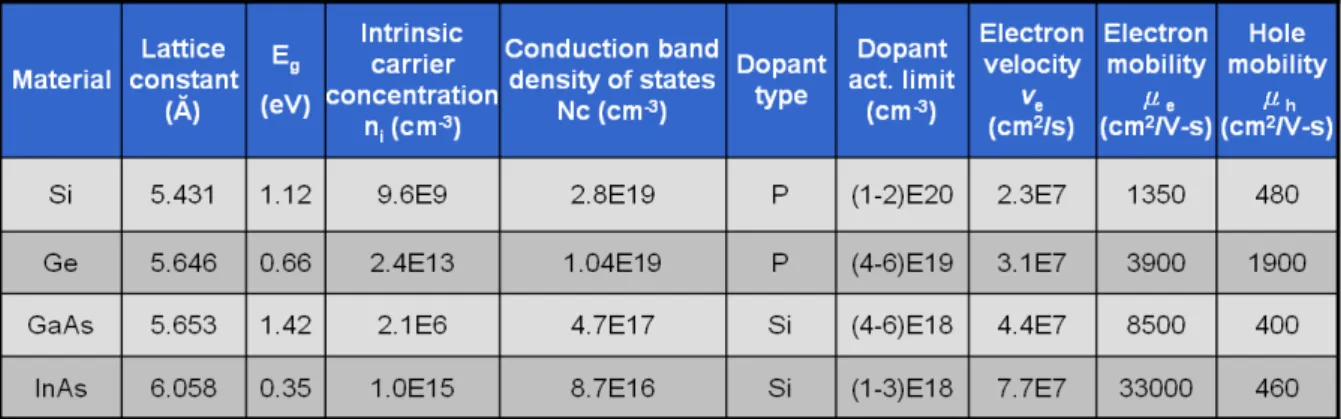
Table. 1.1 Material properties of Si, Ge, GaAs, and InAs at 300 K (p. 11).
Chapter 4
Table. 4.1 Chemical ratios of As 2p3/2 and Ga 2p3/2 spectra for the cleaned GaAs surface
after different WCPs (p. 95).
Chapter 5
Table. 5.1 Chemical ratios of As 2p3/2 and Ga 2p3/2 spectra for the GaAs substrate after
undergoing different wet-chemical procedures. Note that the surface of all samples has been exposed to air for ca. 10 min prior to chemical analysis (p. 123).
Table. 5.2 Calculated relative concentrations of GaAs oxides and stoichiometric O-to-Al ratios in as-deposited ALD-Al2O3 thin films before and after chemical
treatment with (NH4)2S. Note that the As 2p3/2, Ga 2p3/2, Al 2p, and O 1s core
levels were used by considering the atomic sensitivity factor (p. 124).
Table. 5.3 Chemical bonding ratios of As 3d and Ga 3d core levels determined by fitting the XPS data from Fig. 5.5. Note that the contribution of the O 2s emission has been excluded (p. 124).
Table. 5.4 Solid state chemical reactions of Ga–As–O associated systems. All these equations are separated into four parts (p. 125-126).
Table. 5.5 Calculated relative concentration of GaAs oxides and stoichiometric O-to-Al ratios in the N2- and O2-annealed ALD-Al2O3 thin films with and without
Table. 5.6 Chemical bonding ratios of As 3d and Ga 3d core levels determined by fitting the XPS data from Fig. 5.12. Note that the contribution of the O 2s emission has been excluded (p. 127).
Figure Captions
Chapter 1
Fig. 1.1 Transistor scaling and research roadmap demonstrated by R. Chau, Intel Corp, (p. 11).
Fig. 1.2 Scheme of device issues in the nanoscale MOSFETs (p. 12).
Chapter 2
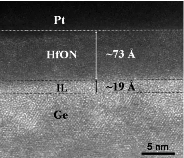
Fig. 2.1 Cross-sectional TEM image of as-deposited Pt/HfOxNy/Ge gate stack (p. 32).
Fig. 2.2 SIMS profiles of as-deposited HfOxNy/Ge gate stack after two different
annealing conditions: (a) 400 °C, 30 s; (b) 500 °C, 5 min (p. 32).
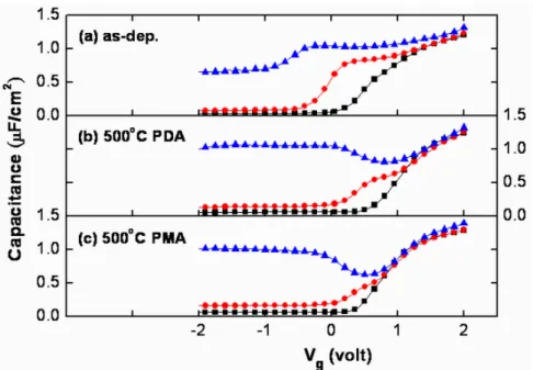
Fig. 2.3 Multi-frequency C–V curves of Pt/HfOxNy/n-Ge capacitors measured at 10
kHz (▲), 100 kHz (●), and 1MHz (■): (a) as-deposited; (b) 500 °C PDA, 30 s;
(c) 500 °C PMA, 30 s (p. 33).
Fig. 2.4 Typical 100-kHz G–V curves of as-deposited and annealed Pt/HfOxNy/n-Ge
capacitors (solid symbols); the annealing duration is 30 s for these two thermal processes. Note that the G–V curve of as-deposited Pt/HfOxNy/n-Si capacitor
(open squares) is added for comparison (p. 33).
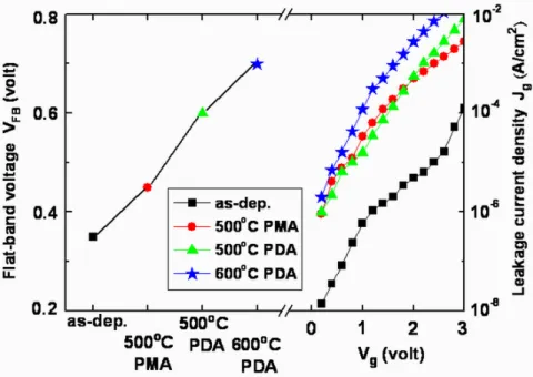
Fig. 2.5 The VFB shift (the left y-axis) and I–V characteristics (the right y-axis) of
Pt/HfOxNy/n-Ge capacitors subjected to different thermal processing (p. 34).
Fig. 2.6 Bidirectional sweep (1 MHz) C–V curves of Pt/HfOxNy/n-Ge capacitors
prepared without (■) and with (△) NH3 nitridation. The inset displays the corresponding plots of Jg versus Vg before and after PDA at 600 °C (p. 34).
Fig. 2.7 Dependence of the hysteresis width in C–V (1 MHz) sweep on the starting accumulation and inversion gate biases; the absence of the hysteresis behavior in the gate-bias ranged from 0 to 1 V (p. 35).
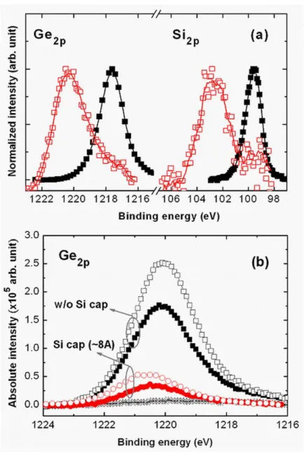
Fig. 2.8 Ge 2p3 XPS spectra of Pt/HfOxNy/Ge capacitors prepared without and with
NH3 nitridation. Three components were extracted: Ge, GeOx, and GeO2 (p.
35).
Fig. 2.9 Ge 3p XPS spectra of Pt/HfOxNy/Ge capacitors prepared without and with NH3
nitridation. Three components were extracted: Ge, GeOx, and GeO2 (p. 36).
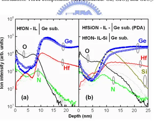
Fig. 2.10 SIMS profiles of HfOxNy thin films deposited on Ge substrates (a) without and
(b) with Si passivation. The solid lines ( — ) and solid squares ( ■ ) refer to
the as-deposited samples; the dotted lines ( --- ) and open squares ( □ ) refer to
the annealed samples (500 °C, 5 min) (p. 36).
Fig. 2.11 (a) XPS spectra displaying the Si 2p and Ge 2p core levels for Ge samples capped with a Si layer (ca. 8 Å) before ( ■ ) and after ( □ ) deposition of the HfOxNy high-k film. (b) Ge 2p spectra of Pt/HfOxNy/Ge gate stacks before
(solid symbols) and after (open symbols) dielectric annealing at 500 °C for 5 min. Note that the lowest curve ( * ) indicates that no Ge was incorporated into the high-k film when thermal processing—PDA and PMA—was not undertaken (p. 37).
Fig. 2.12 Bidirectional sweep (1 MHz) C–V curves of Pt/HfOxNy/Ge gate stacks lacking
and containing a Si capping layer. HfOxNy was the as-deposited thin film and
the capacitors were only subjected to 400 °C PMA (p. 38).
Fig. 2.13 Schematic energy band diagram displaying the charge trapping model for a Pt/HfOxNy/GeOx/Ge gate stack upon (a) sweeping from the inversion bias (Vg
= VFB – 1 V) and (b) sweeping from the accumulation bias (Vg = VFB + 1 V).
Note that the value of VFB was ca. 0.5 V (p. 38).
Chapter 3
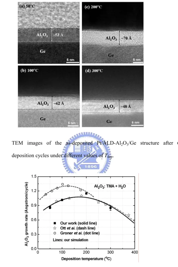
deposition cycles under different values of Tdep (p. 66).
Fig. 3.2 Growth rates of ALD-Al2O3 films plotted against the value of Tdep for both this
and previously studies (by Ott et al. and Groner et al.). Solid lines represented the simulation of our proposed ALD model [25] (p. 66).
Fig. 3.3 (a) Measured and simulated GIXRR curves of the as-deposited Al2O3 (60
cycles)/Ge structures at values of Tdep of 50 and 300 °C. (b) Extracted Al2O3
film densities plotted with respect to the value of Tdep. (c) Extracted
thicknesses of each layer and GeO2/Ge interface roughness plotted against the
value of Tdep. Note that the modeled XRR structure is the
Al2O3/GexAl1-xO/GeO2/Ge gate stack (p. 67).
Fig. 3.4 SIMS depth profiles of carbon second-ion intensity within ALD-Al2O3 (60
cycles) on Ge substrate deposited at various values of Tdep. The Al and O
second-ion intensities of the Al2O3 (Tdep = 300 °C)/Ge sample are labeled as a
reference of the relative depth (p. 68).
Fig. 3.5 (a) Binding energy difference between the peak positions of Al 2p and O 1s core levels for the as-deposited Al2O3 (Tdep = 100 °C)/Ge structure. (b)
Oxygen-to-aluminum elemental ratios estimated from the respective photoemissions of the Al2O3 (Tdep = 50–300 °C)/Ge samples subjected to RTA
at 400 and 600 °C, respectively (p. 68).
Fig. 3.6 (a) Ge 2p3/2 core level spectra of the Al2O3 (Tdep = 100 °C)/Ge structure before
and after RTA. Inset: Emission ratio of Ge oxides to substrate extracted from the Ge 3d core level. (b) Calculated GeO2 atomic concentration within Al2O3
high-k dielectric (Tdep = 50–300 °C) grown on Ge substrate before and after
RTA (p. 69).
Fig. 3.7 (a) Multi-frequency C–V and (b) I–V characteristics of the Pt/Al2O3 (Tdep = 100
C–V curves measured at 100 kHz (p. 70).
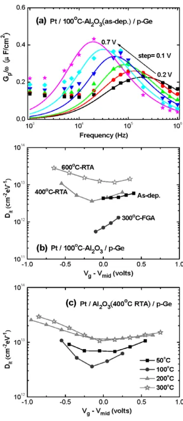
Fig. 3.8 (a) Plot of Gp/ω versus the log frequency curves for the as-deposited Pt/Al2O3
(Tdep = 100 °C)/p-Ge structure under various gate biases. Energy distribution of
Dit for Pt/Al2O3/p-Ge samples (b) subjected to different thermal processing and
(c) grown at values of Tdep from 50 to 300 °C (p. 71).
Fig. 3.9 (a) Equivalent circuit of a p-type MOS device, incorporating the effects of interface states and minority-carrier dart current, which can be characterized by (b) a parallel circuit mode with a frequency-dependent substrate capacitance Csub(w) and conductance Gsub(w). Simplified MOS device circuits biased in (c)
strong accumulation, (d) depletion, and (e) strong inversion (p. 72).
Fig. 3.10 MEDICI-simulated C–V curves of Al/SiO2 gate stacks on Si and Ge substrates
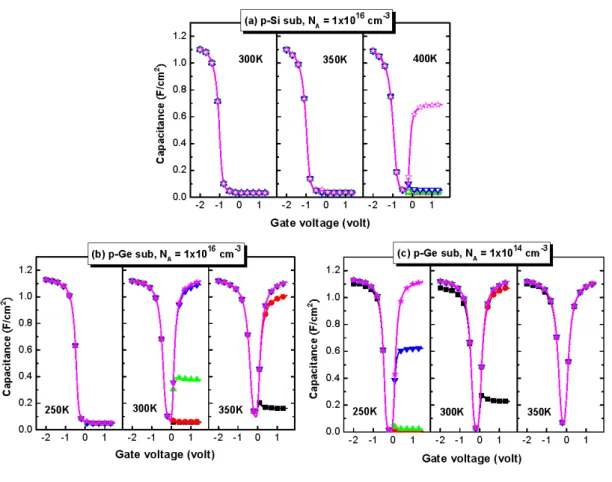
under measured temperatures ranging from 250 to 400 K: (a) p-Si, 1016 cm–3; (b) p-Ge, 1016 cm–3; (c) p-Ge, 1014 cm–3. Note that the measured frequencies are labeled by solid symbols: square (, 1 MHz), circle (z, 100 kHz), up-triangle (▲, 10 kHz), down-triangle (▼, 1 kHz), and star (★, 100 Hz) (p. 73).
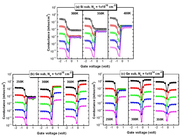
Fig. 3.11 MEDICI-simulated G–V curves of Al/SiO2 gate stacks on Si and Ge substrates
under measured temperatures ranging from 250 to 400 K: (a) p-Si, 1016 cm–3; (b) p-Ge, 1016 cm–3; (c) p-Ge, 1014 cm–3. Note that the measured frequencies are labeled by solid symbols: square (, 1 MHz), circle (z, 100 kHz), up-triangle (▲, 10 kHz), down-triangle (▼, 1 kHz), and star (★, 100 Hz) (p. 74).
Fig. 3.12 Measured C–V (left-hand y-axis) and G–V (right-hand y-axis) curves of Pt/ALD-Al2O3/p-Si MOS capacitors (p. 75).
Fig. 3.13 Measured C–V (left-hand y-axis) and G–V (right-hand y-axis) curves of Pt/ALD-Al2O3/p-Ge MOS capacitors (p. 75).
Fig. 3.14 (a)–(c) C–V and (d)–(f) G–V curves of Pt/ALD-Al2O3/p-Ge MOS capacitors
measured at temperatures of 20, 40, and 60 °C, respectively (p. 76).
Fig. 3.15 (a)–(b) C–V and (c)–(d) G–V curves (1 MHz) of Pt/ALD-Al2O3 gate stacks on
p-Ge and n-Ge MOS capacitors, measured at temperatures ranging from 15 to 100 °C (p. 76).
Fig. 3.16 (a) Simulated Arrhenius-dependent substrate conductances Gsub in Si and Ge at
two dopant concentrations (1014 and 1016 cm–3), plotted with the experimental data obtained in this and previous studies [14], [17]. The simulated Gsub data
can be fitted by the diffusion conductances Gdiff (solid lines) and g-r
conductances Ggr (dashed lines), respectively. (b) Calculations of
temperature-dependent Gdiff and Ggr in Si and Ge substrates having dopant
concentrations of 2 × 1015 cm–3. The values of N
T were 1014 and 1015 cm–3 in Si
and Ge, respectively. The values of the wCinv term were also calculated in
terms of the frequency range 1 kHz–1 MHz (p. 77).
Fig. 3.17 (a) Simulated temperature-dependent transition frequencies ftran in Si and Ge at
two dopant concentrations (1014 and 1016 cm–3), plotted along with our experimental data from Figs. 3.13 and 3.16. (b) Calculated temperature-dependent transition frequencies ftran in Si and Ge substrates,
determined according to the material parameters in Fig. 3.19. Different values of NT (1017–1019 cm–3) were assumed for our highly doped Ge system (p. 78).
Fig. 3.18 (a) Calculated response frequency fit of interface states plotted as a function of
the surface potential φS for Si and Ge capacitors at RT. (b) Temperature
dependence of the plots of fit versus the φS for the Ge capacitor. The shadow
region represents the standard frequency range 1 kHz–1 MHz used for measurements. (c) Plot of the φS dependence of observable Dit in the Ge
range). For comparison, the temperature dependence of the Ge bandgap is presented on the right-hand y-axis (p. 79).
Fig. 3.19 Measured values of Gsub/w plotted with respect to the log frequency for
Pt/ALD-Al2O3 gate stacks on (a)–(c) p-Ge and (d)–(f) n-Ge substrates at
temperatures of 20, 40, and 60 °C, respectively (p. 80).
Chapter 4
Fig. 4.1 As 2p3/2 XPS spectra of clean GaAs substrate subjected to four different WCPs.
Five components were extracted: GaAs, AsSx, As2O3, As2O5, and elemental As
(p. 95).
Fig. 4.2 Ga 2p3/2 XPS spectra of clean GaAs substrate subjected to four different WCPs.
Four components were extracted: GaAs, GaSx, Ga2O, and Ga2O3 (p. 96).
Fig. 4.3 RMS surface roughness of clean GaAs substrate subjected to different WCPs (p. 96).
Fig. 4.4 (a) Bidirectional sweep (10 kHz) C–V curves; (b) the frequency response of
△C and △V values for Pt/Gd2O3/n-GaAs capacitors with four kinds of WCPs
(p. 97).
Fig. 4.5 The I–V characteristics of Pt/Gd2O3/n-GaAs capacitor with the WCP ― HCl +
NH4OH + Sulfide (1%, 80 °C). The inset displays the plot of Jg@ Vg = (VFB +
1) V versus the WCP conditions (p. 98).
Fig. 4.6 As 2p3/2 and Ga 2p3/2 XPS spectra of the Pt/Gd2O3/GaAs structures
investigated in Figs. 4.4 and 4.5 (p. 98).
Fig. 4.7 Comparison of Jg versus CET or EOT characteristics for Pt/Gd2O3/n-GaAs
Chapter 5
Fig. 5.1 (a) Multi-frequency C-V and (b) bidirectional C-V (10 kHz) curves of Pt/ALD-Al2O3/n+-GaAs capacitors with different cleaning preparation and
annealing processes. The Al2O3 films were deposited at 100 °C for 60 cycles (p.
128).
Fig. 5.2 Gate leakage current Jg characteristics of Pt/Al2O3/n-GaAs capacitors. The
Al2O3 thin films were deposited at 100 °C for 60 cycles (p. 128).
Fig. 5.3 (a) C-V curves of GaAs MOS capacitors with ALD-Al2O3 deposited at 300°C
for 60 cycles and (b) Comparison of Jg versus CET characteristics of
ALD-Al2O3/GaAs capacitors deposited at 100 and 300 °C with different
surface preparation and annealing processes (p. 129).
Fig. 5.4 As 2p3/2 and Ga 2p3/2 XPS spectra of as-deposited ALD-Al2O3 thin films on
GaAs substrates without and with (NH4)2S sulfide passivation (p. 130).
Fig. 5.5 As 3d and Ga 3d XPS spectra of as-deposited ALD-Al2O3 thin films on GaAs
substrates with and without (NH4)2S sulfide passivation (p. 130).
Fig. 5.6 (a) Multi-frequency and (b) bi-directional C–V characteristics and (c) gate leakage current (I–V) curves of GaAs MOS capacitors with as-deposited Al2O3
thin films after (NH4)2S passivation and PMA at 400 °C (p. 131).
Fig. 5.7 HRTEM images of Pt/Al2O3/sulfidized-GaAs structures with different
deposition cycles and PDA conditions: (a) 100 cycles, N2 PDA; (b) 100 cycles,
O2 PDA; (c) 60 cycles, O2 PDA. PDA temperature: 600 °C (p. 132).
Fig. 5.8 Multi-frequency C–V curves of sulfidized-GaAs MOS capacitors with Al2O3
thin films annealed for (a) 100 and (b) 60 deposition cycles. Each inset displays the respective C–V hysteresis measured at 100 kHz (p. 133).
Fig. 5.9 I–V Characteristics of the MOS capacitors analyzed in Fig. 5.8. Inset: Plot of Jg
Fig. 5.10 Stress time dependence of the gate leakage Jg for Pt/ALD-Al2O3/GaAs MOS
capacitors under a constant Vg stress of 5 V (at the left y-axis) and a constant Eox stress of 8.5 MV cm–1 (at the right y-axis), respectively (p. 134).
Fig. 5.11 As 2p3/2 and Ga 2p3/2 XPS spectra of 600 °C-annealed Al2O3 thin films on the
sulfidized GaAs substrate. The contributing chemical components were extracted and are displayed in the respective spectra (p. 135).
Fig. 5.12 As 3d and Ga 3d XPS spectra of 600 °C-annealed Al2O3 thin films on the
sulfidized GaAs substrate. The contributed chemical components were extracted and are displayed in the respective spectra (p. 136).
Fig. 5.13 SIMS depth profiles of the Al2O3/GaAs samples analyzed in Fig. 5.12. The
diffusion of As- and Ga-related chemical species into overlying high-k film was observed (p. 136).
Fig. 5.14 Ga 2p3/2 and As 2p3/2 XPS spectra of GaAs substrate subjected to different
wet-chemical procedures. Four components were extracted in Ga 2p3/2 spectra:
GaAs, GaSx, Ga2O, and Ga2O3, while five components were extracted in As
2p3/2 spectra: GaAs, elemental As, AsSx, As2O3, and As2O5 (p. 137).
Fig. 5.15 AFM images of the NH4OH-cleaned GaAs substrates (a) before and (b) after
receiving (NH4)2S-C4H9OH(10%, 60 °C) chemical treatment, respectively (p.
138).
Fig. 5.16 TEM image of the as-deposited Pt/ALD-Al2O3(60 deposition cycles)/GaAs
MOS structure with (NH4)2S-C4H9OH(10%, RT) chemical treatment (p. 138).
Fig. 5.17 Multi-frequency C–V curves of Pt/Al2O3/n-GaAs capacitors (a) with different
wet-chemical procedures; (b) before and after 600 °C PDA. (c) Variations of the frequency response of △C and △V values (p. 139).
Fig. 5.18 (a) The I–V characteristics of Pt/Al2O3/n-GaAs capacitors with various
PDA in O2 ambient, respectively. (b) Comparison of Jg versus CET or EOT
characteristics for our work with other’s published data [2], [6], [48]-[51] (p. 140).
Chapter 6
Fig. 6.1 Scheme of the depletion-mode GaAs n-MOSFET structure (p. 163).
Fig. 6.2 I–V characteristics of p+n junctions activated at 500 °C, before and after performing FGA. Inset: Weibull plot of the value of JR at VR = –1 V (p. 163).
Fig. 6.3 Effects of FGA at 300 °C on the (a) Ids–Vgs and (b) Ids–Vds characteristics of
ALD-Al2O3/Ge p-FETs (W/L = 100 μm/4 μm) (p. 164).
Fig. 6.4 NBTI characteristics of ALD-Al2O3/Ge p-FETs prepared with and without
FGA at 300 °C (p. 165).
Fig. 6.5 Effective hole mobility of ALD-Al2O3/Ge p-FETs plotted with respect to the
effective field; published mobility data are also presented [7], [33] (p. 165). Fig. 6.6 Effects of activation conditions and SiO2 capping layer on the n+p junction
characteristics: (a) 500–700 °C, 30 s, without SiO2; (b) 600–700 °C, 30 s, with
SiO2; (c) 700 °C, 30–90 s, with SiO2 (p. 166).
Fig. 6.7 SIMS depth profiles of the P-implanted Ge junctions discussed in Fig. 5: (a) 500–700 °C, without SiO2; (b) 600–700 °C, with SiO2; (c) 30–90 s, with and
without SiO2. Inset: Expanded image of the SIMS profile at the surface region
(<100 nm) (p. 167).
Fig. 6.8 (a) Schematic representation of the contact and transport resistances between two Al metal pads within the same P-implanted region. (b) Extraction of the values of Rtotal, Rtran, and Rcont under various activation conditions and SiO2
capping effects. The gray region labels are values equal to two times the respective values of Rcont (i.e., 2Rcont) (p. 168).
diode perimeter. (c) Extraction of the perimeter leakage component Jp as
functions of the activation conditions and SiO2 capping effects. Inset:
Schematic representation of the two main leakage paths (Jp and JA) at the S/D
contact region; JA comprises the generation-recombination current (Jgr) and
diffusion current (Jdiff) (p. 169).
Fig. 6.10 Effects of FGA at 300 °C on the (a) Ids–Vgs and (b) Ids–Vds characteristics of
ALD-Al2O3/Ge n-FETs (W/L = 100 μm/8.8 μm) (p. 170).
Fig. 6.11 Effective electron mobility of ALD-Al2O3/Ge n-FETs plotted with respect to
the effective field; published mobility data are also presented [33], [42], [43] (p. 171).
Fig. 6.12 AES depth profiles of the Au/Ge/Ni S/D Ohmic contact (a) before and (b) after 400 °C for 1 min, respectively (p. 171).
Fig. 6.13 TEM images of (a) the D-mode GaAs n-MOSFET structure; (b) alloyed Ni/Ge/Au S/D Ohmic contact after 400 °C for 1 min; (c) Al/ALD-Al2O3/GaAs
channel, respectively (p. 172).
Fig. 6.14 (a) Id–Vg and (b) Id–Vd characteristics of the D-mode ALD-Al2O3/GaAs
n-MOSFET with (NH4)2S-C4H9OH chemical treatment, respectively (p. 173).
Chapter 1
Introduction and Research Motivation
1.1 Overview
of
Transistor
Research Roadmap and Device
Scaling Issues
The rapid advancement of complementary metal oxide semiconductor (CMOS) integrated circuit technologies during the past few decades has forced the Si-based microelectronics industry to face several huge technological challenges and to test some theoretical limits. R. Chau, Intel Corporation, has even demonstrated the scaling roadmap in the progress of the Si MOS field-effect-transistors (FETs), as displayed in Fig. 1.1. It was found that within the next two decades, the lateral dimensions of the transistor will approach the physical limits and finally consist of only a few atoms. Accordingly, several device issues emerged in the nanoscale MOSFETs, as the scheme presented in Fig. 1.2. The first issue is the poor device electrostatics and we need to maintain the gate control ability within the channel. One solution is the use of the double- and triple-gates to improve the electrostatics, but, it also implies that the additional process challenges emerged in such new device architecture. Second, the channel transport characteristic is also degraded, leading to the decrease of device on-current (Ion). Employment of new channel materials possessing the higher carrier mobility
and injection velocity is conceivable to solve this channel issue, even if these materials possibly bring other integration issues in Si device platform. Third, it is expect that the impact of the source/drain (S/D) resistance on the reduction of Ion is an increasing importance with
the dimension scaling. It was suggested that the replacement of the ion implantation with the in-situ doping in the S/D region, i.e., implantation-free S/D, or the use of metal Schottky S/D is the possible solution to reduce the effect of the extrinsic resistance. The fourth and fifth
issues are an exponential increase in the gate leakage current of an ultra-thin SiO2 and the
poly depletion effect, respectively. Even up to now, these two well-known issues are of intense discussion. Of course, the adoption of the metal-gate/high-k dielectric stack is the optimum solution to solve these two issues.
In fact, at the early stage of the 90-nm node, substrate engineering and uniaxial strain technologies—e.g., pseudomorphic SiGe channels grown on the Si substrates for p-FETs [1] and strained Si channels on the relaxed graded SiGe buffer layers for n-FETs [2]—have been developed to enhance the carrier mobility in the channel. With further scaling down to the 45-nm node, high-k materials are also introduced as alternative gate dielectrics—in place of ultra-thin conventional SiO2 or oxynitrides—in light of leakage concerns and reliability issues.
Many novel device structures and materials are continuously proposed and explored eagerly in an effort to alleviate the tremendous scaling pressure required to improve device performances. Various kinds of non-planar tri-gate architectures, carbon nanotubes, nanowires, and high-mobility materials catch an increasing attention in recent years. Among above intense researches, the feasibility of integrating various prevailing high-k dielectrics with high mobility substrates is of much interest due to the advanced progress in the development of high-k dielectrics in Si-based MOSFET applications. Through the Table 1.1, we can compare the material properties of bulk Si, Ge, GaAs, and InAs at 300 K [3]. As seen, since Ge possesses the higher electron (3×) and hole (4×) mobilities than those in Si, therefore, Ge is considered new potential candidate to be p- and n-channel materials for high-performance logic devices. While GaAs and InAs, relative to Si, have the advantages of much higher enhancements in electron mobility and velocity; in consequence, III-V materials are suitable to be n-channel MOSFET. Up to date, the promising device characteristics of Ge [4], [5], (In)GaAs [6], and InSb [7] channels with either HfO2 or Al2O3 high-k dielectrics have been
continually demonstrated, and their performance even surpassed the traditional Si transistors at the sub-micro gate length [8]. Therefore, it is believed that the MOS capacitor and device
properties integrating various high-k dielectric materials onto Ge and GaAs substrates are worthy to study in this dissertation. Accordingly, the device challenges and process difficulties in use of the high-mobility channels/substrates are of importance to describe more details. We will describe these subjects in the following Session 1.2.
1.2
Device and Process Challenges in High Mobility Substrates
As discussed in the previous section, great progress in the deposition of high-k materials enables renewed interest in high-mobility substrates being as a transport channel in combination with various high-k dielectrics. In other words, the first challenge is how to realize the high interface quality between the deposited dielectric films and either Ge or III-V semiconductors. The absence of thermodynamically stable insulators on these two high-mobility substrates has probably become the foremost bottleneck to them rivaling or exceeding the properties of Si MOSFETs. This actually leads to the onset of high interfacial state density (Dit), thereby causing a Fermi level (Ef) pinning effect and casting some doubts
on the anticipated performance [9]. In fact, for the studies of the dielectric/III-V interface, especially the (In)GaAs substrate, numerous efforts have been devoted for more than four decades in intensively questing the competitive, high interface quality insulators and efficient passivation methods, respectively. Except for SiO2 and Si3N4, (Gd,Ga)2O3 and
atomic-layer-deposited (ALD) Al2O3 [10], HfO2 [11] high-k dielectrics are of particular
interest; meanwhile, the sulfur chemical treatment [12], and Si and Ge [13] as the interfacial passivation layers are currently active approaches to protect the III-V surface prior to the dielectric deposition. Namely, Ge also requires the surface protection, like employing the thermal annealing in NH3 [14] or SiH4 [15] ambient, in order to reduce the value of the Dit as
Another important subject is the fabrication of high-performance S/D junction in Ge and III-V MOSFETs. At first, for the Ge p+n junction, fortunately, the boron is a highly activated dopant without the need of higher annealing temperature (just in the range 450–550 °C), and the retarded diffusion behavior of boron dopant is also observed [16]. However, almost the opposed results are characterized in the corresponding n+p junction. Not only a higher thermal budget (in the range 550–650 °C) is required during n-type dopant activation, but also more rapid dopant diffusion (either out of the surface or into the substrate) and lower electrical activation are generally observed [17], [18]. It has been reported previously that the amounts of P dopant loss were ca. 40% and >60% after RTA at 500 and 600 °C, respectively [19]. The resultant surface concentration also influenced the variation of the contact resistance [20]. Therefore, how to obtain the n+p shallow junction having an acceptable leakage current is critical to obtaining high-performance Ge n-FETs. It should be noted that the feature of small bandgap in Ge and other III-V materials (except GaAs) is likely to give rise to high band-to-band tunneling (BTBT) leakage current and hence large static power dissipation.
On the other hand, the III-V junction diodes have been widely investigated because of the optoelectronic applications, but, we still need to consider two essential issues in fabricating the III-V n+p junction for the n-FET application. One is that the dopant activation temperature, in general, is also higher, e.g, in the range 750–850 °C for (In)GaAs-based materials, which in turn possibly degrades the characteristic of the dielectric/III-V interface. Another is III-V materials that usually possess the lower values of solid solubility of n-type dopants and the density of states (DOS), as shown in Table 1.1. For example, in GaAs the maximum Si solubility and the DOS are merely (4-6) × 1018 and 4.7 × 1017 cm-3, respectively, which are ca. 1.5 and 2 orders of magnitude lower than those in Si. In consequence, these inherent material issues certainly contribute the more S/D resistance in device and hence limit the maximum Ion, acting the obstacle in outperforming the Si device performance of deep
Other device issues and process difficulties, like the work function of gate metals, the metal germanide technology in S/D, wet-chemical cleaning processes, and wet/dry etching, are still significant. Most importantly, the subject of heterogeneous integration of these Ge and III-V materials onto the traditional Si platform, i.e., the heteroepitaxy technique, will be quite critical in developing these oncoming nanoscale CMOS technologies.
1.3
Scope and Organization of the Thesis
Two promising high-mobility substrate materials, Ge and GaAs, are investigated in this dissertation. We devoted our efforts to the effects of wet-chemical clean, surface passivation, and thermal processing on the physical and electrical properties of various alternative high-k gate dielectrics on these two substrates. This dissertation is divided into seven chapters and organized as follows:
In Chapter 1, a brief overview of the background and motivation is described. We reviewed the MOSFET scaling roadmap and the possible challenges emerged in the nanoscale devices. Next, we discussed the significance of high mobility substrates in further application of the advanced CMOS technologies; meanwhile, the process difficulties and material issues in the accomplishment of the Ge and GaAs III-V devices were brought up.
In Chapter 2, we performed the physical and electrical analyses to systematically examine the HfOxNy thin films sputtered on Ge substrates and the admittance properties of
their MIS capacitors. Both the NH3 plasma treatment and Si2H6 thermal annealing are
proposed in an attempt to improve the properties of HfOxNy high-k films on Ge substrates.
We observed that not only the out-diffusion of Ge substrate and charge trapping phenomenon of entire HfOxNy/Ge gate stack are relieved, but also the thermal stability is enhanced after
these two passivation methods.
grown through ALD system on Ge substrates. It was observed that variation of the substrate temperature strongly influenced the Al2O3 film qualities on Ge, including the density,
stoichiometry, and the degree of the Al2O3-GeO2 intermixing. Such a temperature effect on
the interface, capacitor, and gate leakage characteristics of the Al2O3/Ge structures is
examined as well. Furthermore, we explored the minority-carrier response behavior of Ge MOS capacitors through MEDICI simulations and device experiments, and further compare their electrical differences with those in traditional Si MOS capacitors.
In Chapter 4, we modified the wet-chemical clean and (NH4)2S sulfidizing treatment on
GaAs substrate and characterized the effects of the surface modification on the interfacial and electrical improvements of the e-gun evaporated Gd2O3/GaAs MOS capacitors. In addition,
we further compared the gate leakage characteristics of the fabricated Gd2O3/GaAs structures
to the reported performance of various high-k dielectric materials on GaAs substrates.
In Chapter 5, the deposition of ALD-Al2O3 gate dielectrics on GaAs substrates was
studied. Next, the impact of interfacial (NH4)2S treatment integrating with different
sulfidizing solvents was investigated through analyses of the surface chemistry and capacitor characteristics of the Al2O3/GaAs structure. In the following, we performed the
post-deposition annealing in O2 and N2 ambient to understand the changes of the structural
and electrical properties; the differences were clarified in terms of identifying the underlying thermochemical mechanisms.
In Chapter 6, both the inversion-mode Ge p- and n-MOSFETs and the depletion-mode GaAs n-MOSFET with the ALD-Al2O3 gate dielectrics were fabricated. Herein, we studied
effects of the forming gas annealing on the Ge junction and device properties; the correlation between the n-type dopant activation and the origins of n+p junction leakage and source/drain resistance is also analyzed in more details. On the other hand, the transfer and output characteristics of ALD-Al2O3/GaAs n-MOSFET were demonstrated and we employed the
In Chapter 7, we summarized the experimental results in the thesis and gave the conclusions and the suggestions for future studies.
References (Chapter 1)
[1] C.-W. Chen, C.-H. Chien, Y.-C. Chen, S.-L. Hsu, and C.-Y. Chang, “Deep sub-micron strained Si0.85Ge0.15 channel p-channel metal-oxide-semiconductor field-effect transistors
(pMOSFETs) with ultra-thin N2O-annealed SiN gate dielectric,” Jpn. J. Appl. Phys., vol.
44, p. L278, 2005.
[2] N. Sugii, D. Hisamoto, K. Washio, N. Yokoyama, and S. Kimura, “Performance enhancement of strained-Si MOSFETs fabricated on a chemical-mechanical-polished SiGe substrate,” IEEE Trans. Electron Devices, vol. 49, p. 2237, 2002.
[3] M. Levinshtein, S. Rumyantsev, and M. Shur, Handbook Series on Semiconductor Parameters Volume 1: Si, Ge, C(diamond), GaAs, GaP, GaSb, InAs, InP, InSb, World
Scientific, Singapore, 1996.
[4] D. Kuzum, A. J. Pethe, T. Krishnamohan, and K. C. Saraswat, “Ge (100) and (111) n- and p-FETs with high mobility and low-T mobility characterization,” IEEE Trans. Electron Devices, vol. 56, p. 648, 2009.
[5] G. Nicholas, B. De Jaeger, D. P. Brunco, P. Zimmerman, G. Eneman, K. Martens, M. Meuris, and M. M. Heyns, “High-performance deep submicron Ge pMOSFETs with halo implants,” IEEE Trans. Electron Devices, vol. 54, p. 2503, 2007.
[6] H.-C. Chin, M. Zhu, Z.-C. Lee, X. Liu, K.-M. Tan, H. K. Lee, L. Shi, L.-J. Tang, C.-H. Tung, G.-Q. Lo, L.-S. Tan, and Y.-C. Yeo, “A new silane-ammonia surface passivation technology for realizing inversion-type surface-channel GaAs n-MOSFET with 160 nm gate length and high-quality metal-gate/high-k dielectric stack,” Tech. Dig. Int. Electron Devices Meet., p. 383, 2008.
[7] N. Goel, D. Heh, S. Koveshnikov, I. Ok, S. Oktyabrsky, V. Tokranov, R. Kambhampati, M. Yakimov, Y. Sun, P. Pianetta, C.K. Gaspe, M.B. Santos, J. Lee, S. Datta, P. Majhi, and W. Tsai, “Addressing the gate stack challenge for high mobility InxGa1-xAs channels for
nFETs,” Tech. Dig. Int. Electron Devices Meet., p. 363, 2008.
[8] M. Radosavljevic, T. Ashley, A. Andreev, S. D. Coomber, G. Dewey, M. T. Emeny, M. Fearn, D. G. Hayes, K. P. Hilton, M. K. Hudait, R. Jefferies, T. Martin, R. Pillarisetty, W. Rachmady, T. Rakshit, S. J. Smith, M. J. Uren, D. J. Wallis, P. J. Wilding and R. Chau, “High-performance 40nm gate length InSb p-channel compressively strained quantum well field effect transistors for low-power (Vcc=0.5V) logic applications,” Tech. Dig. Int. Electron Devices Meet., p. 727, 2008.
[9] T. H. Chiang, W. C. Lee, T. D. Lin, D. Lin, K. H. Shiu, J. Kwo, W. E. Wang, W. Tsai, and M. Hong, “Appoaching Fermi level unpinning in oxide-In0.2Ga0.8As,” Tech. Dig. Int.
Electron Devices Meet., p. 375, 2008.
[10] H.-L. Lu, L. Sun, S.-J. Ding, M. Xu, D. W. Zhang, and L.-K. Wang, “Characterization of atomic-layer-deposited Al2O3/GaAs interface improved by NH3 plasma pretreatment,”
Appl. Phys. Lett. vol. 89, p. 152910, 2006.
[11] M. Zhu, C.-H. Tung, and Y.-C. Yeo, “Aluminum oxynitride interfacial passivation layer for high-permittivity gate dielectric stack on gallium arsenide,” Appl. Phys. Lett. vol. 89, p. 202903, 2006.
[12] M.-K. Lee, C.-F. Yen, J.-J. Huang, and S.-H. Lin, “Electrical characteristics of postmetallization-annealed MOCVD-TiO2 films on ammonium sulfide-treated GaAs,” J.
Electrochem. Soc. vol. 153, p. F266, 2006.
[13] H.-S. Kim, I. Ok. M. Zhang, T. Lee, F. Zhu, L. Yu, and J. C. Lee, “Metal gate-HfO2
metal-oxide-semiconductor capacitors on n-GaAs substrate with silicon/germanium interfacial passivation layers,” Appl. Phys. Lett. vol. 89, p. 222903, 2006.
[14] T. Maeda, M. Nishizawa, Y. Morita, and S. Takagi, “Role of germanium nitride interfacial layers in HfO2/germanium nitride/germanium metal-insulator-semiconductor
[15] N. Wu, Q. Zhang, D. S. H. Chan, N. Balasubramanian, and C. Zhu, “Gate-first Germanium nMOSFET with CVD HfO2 gate dielectric and silicon surface passivation,”
IEEE Electron Devices Lett., vol. 27, p. 479, 2006.
[16] Y. S. Suh, M. S. Carroll, R. A. Levy, G. Bisognin, D. D. Salvador, M. A. Sahiner, and C. A. King, “Implantation and activation of high concentrations of boron in germanium,” IEEE Trans. Electron Devices, vol. 52, p. 2416, 2005.
[17] M. Posselt, B. Schmidt, W. Anwand, R. Grotzschel, V. Heera, A. Mucklich, C. Wundisch, W. Skorupa, H. Hortenbach, S. Gennaro et al., “P implantation into preamorphized germanium and subsequent annealing: solid phase epitaxial regrowth, P diffusion, and activation,” J. Vac. Sci. Technol. B, vol. 26, p. 430, 2008.
[18] A. Satta, E. Simoen, R. Duffy, T. Janssens, T. Clarysse, A. Benedetti, M. Meuris, and W. Vandervorst, “Diffusion, activation, and recrystallization of high dose P implants in Ge,” Appl. Phys. Lett., vol. 88, p. 162118, 2006.
[19] A. Satta, T. Janssens, T. Clarysse, E. Simoen, M. Meuris, A. Benedetti, I. Hoflijk, B. D. Jaeger, C. Demeurisse, and W. Vandervorst, “P implantation doping of Ge: diffusion, activation, and recrystallization,” J. Vac. Sci. Technol. B, vol. 24, p. 494, 2006.
[20] C.-C. Cheng, C.-H. Chien, G.-L. Luo, C.-L. Lin, H.-S. Chen, J.-C. Liu, C.-C. Kei, C.-N. Hsiao, and C.-Y. Chang, “Junction and Device Characteristics of Gate-Last Ge p- and n-MOSFETs with ALD-Al2O3 Gate Dielectric,” IEEE Trans. Electron Devices,
(accepted).
[21] M. V. Fischetti, L. Wang, B. Yu, C. Sachs, P. M. Asbeck, Y. Taur, and M. Rodwell: ‘Simulation of electron transport in high-mobility MOSFETs: density of states bottleneck and source starvation’, Int. Electron Devices Meet. Tech. Dig., p. 109, 2007.
Table. 1.1 Material properties of Si, Ge, GaAs, and InAs at 300 K.
Fig. 1.1 Transistor scaling and research roadmap demonstrated by R. Chau, Intel Corp.
Chapter 2
Sputtered HfO
xN
yDielectric Films on Bulk Ge Substrates
2.1
Introduction
Recently, Ge-channel devices—including bulk Ge [1], [2], strained Ge [3], and Ge-on-insulator (GOI) [4] systems—integrated with high-k gate dielectrics have attracted considerable research interest. Although transistors were originally fabricated on Ge substrates, the lack of a stable Ge native oxide has been an obstacle in complementary metal-oxide-semiconductor (CMOS) device realization with Ge. Therefore, silicon has been used in CMOS technology for many decades because of the better qualities of its native oxide, such as a low leakage current, low interface state density, and good thermal stability. With the further scaling of device and gate oxide dimensions down to the nanometer range, however, the leakage current density in SiO2 has become much higher than 2 mA/cm2, which is the
maximum concession for low power applications [5]. Consequently, higher dielectric-constant materials with a thicker physical thickness are introduced to suppress the concern of excessive gate leakage while maintaining the equivalent-oxide-thickness (EOT) of the scaled devices.
Presently, hafnium-based oxides or oxynitrides, e.g., HfO2, HfON, and HfSiON, are the
uppermost candidates for application among all of the potential high-k dielectrics. Both Si and SiGe MOSFETs integrated with Hf-based gate dielectrics exhibit admirable properties [6]-[8], but they also reveal undesirable surface carrier mobility degradation behavior [9], [10]. Changing the substrate from Si to Ge might be a possible solution to this problem because Ge has a higher carrier mobility relative to that of Si. From recent advances in the deposition of high-k materials, Ge MOSFETs incorporating high-k gate dielectrics have exhibited some promising performance [11], [12]. In this session, we investigated the physical and electrical
characteristics of HfOxNy sputtered films on bulk Ge substrates and then determined the
impact of thermal annealing processing on the entire capacitor structure. Meanwhile, recent reports have described that annealing a cleaned Ge substrate in a NH3 [13] or SiH4 [14] gas
ambient, prior to deposition of a high-k dielectric, further improves the MOS properties on Ge. Here, we proposed the NH3 plasma pretreatment to passivate a Ge substrate and investigated
the passivation efficiency. Actually, the overall MOS structures had higher thermal stability and showed the improved electrical characteristics. On the other hand, we also speculate that the incorporation of nitrogen atoms may lead to incomplete passivation of the dangling bonds on the Ge surface; such a surface would not fully inhibit the growth of GeOx because of the
lower thermal stability of Ge–N bonds [15]. Therefore, we also attempted to adopt the Si2H6
passivation onto Ge surfaces, in which several monolayers of Si exist between the gate dielectric and Ge substrate, for inhibiting the formation of GeOx and suppressing hysteresis
phenomena in high-k/Ge MOS capacitors; we also presented an energy band diagram to explain the charge trapping model.
2.2
Experimental Procedures
N-type Ge substrates, which were doped with Sb dopant at a concentration of ca. 1 × 1014 cm–3 (resistivity ~ 8–12 Ω·cm), were precleaned through a cyclic rinse involving a diluted HF dip and deionized water. After wet cleaning, the NH3 plasma exposure on the Ge
surface of some samples was performed in the plasma-enhanced chemical vapor deposition (PECVD). HfOxNy thin films were subsequently deposited through reactive sputtering in a
Ar+N2 ambient with a pure Hf target, followed by annealing in a N2 atmosphere containing
residual oxygen. In an attempt to suppress any additional oxidation, which can help to minimize the thickness of interfacial layer (IL), the post-deposition annealing (PDA) was performed in an N2 ambient rather than an O2 ambient to convert HfN into HfOxNy. Various
PDA temperatures (500 and 600 °C) and durations (30 s and 5 min) were employed. Next, a platinum (Pt) dot was deposited using electron beam evaporation through a shadow mask. For evaluating the thermal stability of the Pt/high-k/Ge structures, the post-metallization annealing (PMA) with the same temperature conditions were performed.
For experiments of the ultrathin Si capping, the cleaned Ge substrates underwent thermal desorption at 550 °C for 10 min through ultrahigh-vacuum chemical vapor deposition (UHVCVD) to remove the native GeOx, followed by in situ passivation of a Si capping layer
upon annealing under a Si2H6 ambient at the same substrate temperature; the
thicknesses—evaluated using angle-resolved x-ray photoelectron spectroscopy (AR-XPS)—were ca. 8 Å and ca. 13 Å for annealing duration of 1 and 2 min, respectively. After the following deposition of high-k film and metallization process, the Pt/HfOxNy/Ge
MOS capacitor structure can be obtained.
Transmission electron microscopy (TEM) and secondary ion mass spectroscopy (SIMS) were employed to investigate the entire structure and Ge incorporation behavior after these two pretreatments, respectively. In addition, we carried out ex-situ XPS measurements using an Al Kα source (1486.6 eV) to examine the effects of surface plasma nitridation on the dielectric-substrate interface and evaluate the Ge contamination level within the top high-k films. In electrical characterization, the capacitance−voltage (C−V) and conductance−voltage (G–V) curves were measured using an HP4284 LCR meter, while the current−voltage (I−V) characteristics were measured using a Keithley 4200 semiconductor analyzer system. We further extracted the series resistance and external inductance or capacitance in measurements and then applied as a correction to the measured capacitance and conductance [16], [17]. The value of the effective trapped charge density (Neff) was determined quantitatively by
measuring the hysteresis width at flat-band voltage (VFB) in the bidirectional C–V sweeps [18].