國 立 交 通 大 學
電子工程學系電子研究所
博 士 論 文
低介電常數材料應用於多層導體連線
之電特性分析
Electrical Characteristics Study of Low Dielectric
Constant Materials in Multilevel Interconnect
System
研 究 生:方 國 龍
指導教授:崔 秉 鉞
陳 茂 傑
低
低介
介
電常
電
常數
數材
材料
料
應用
應
用於
於多
多層
層
導體
導
體連
連線
線
之電
之
電特
特性
性分
分
析
析
E
El
le
e
ct
c
tr
ri
ic
ca
al
l
C
C
ha
h
ar
ra
a
ct
c
te
e
ri
r
is
st
ti
ic
cs
s
S
St
tu
u
dy
d
y
o
of
f
L
L
ow
o
w
D
Di
i
el
e
le
e
ct
c
tr
ri
i
c
c
C
C
on
o
ns
st
ta
an
nt
t
M
Ma
a
te
t
e
ri
r
ia
al
ls
s
i
i
n
n
M
Mu
u
lt
l
ti
il
le
e
ve
v
el
l
I
In
nt
te
er
rc
co
on
n
ne
n
ec
ct
t
S
Sy
ys
st
te
em
m
研 究 生
: 方國龍 Student : Kuo-Lung Fang
指導教授
: 崔秉鉞 Advisor : Bing-Yue Tsui
陳茂傑 Advisor : Mao-Chieh Chen
國立交通大學
電子工程學系 電子研究所
博士論文
A Dissertation
Submitted to Department of Electronics Engineering
and Institute of Electronics
College of Electrical Engineering and Computer Science
National Chiao-Tung University
In Partial Fulfillment of the Requirements
for the Degree of
Doctor of Philosophy
in Electronics Engineering
2004
Hsinchu, Taiwan, Republic of China
低介電常數材料應用於多層導體連線
之電特性分析
研 究 生: 方 國 龍
指導教授: 崔 秉 鉞 博士
陳 茂 傑 博士
國 立 交 通 大 學
電子工程學系 電子研究所
摘要 本論文研究積體電路製造技術中的低介電常數材料與多層銅導線連線整合 製程之電特性分析及其相關技術之研究,並探討低介電常數材料應用於下一世代 積體電路高頻訊號傳導的可能性。研究對象除了最成熟的 Fluorosilicate Glass (FSG)外,還包括多孔隙型低介電常數材料如有機類的 Nano-porous Carbon doped Oxide (CDO)以及旋轉塗佈型的 Porous SiLK,以及低介電常數阻障層碳化矽 (SiC)。FSG 是一含氟的氧化矽合物,主要以化學氣相沈積生成,是最接近傳統積體 電路製程中二氧化矽的低介電膜,雖然介電係數約 3.6,卻是目前唯一明確應用
於積體電路量產的材料,因此利用 FSG 來討論其它各種低介電常數材料在整合 製程時,因製程不同造成介電質表面損傷時,所需注意金屬離子擴散問題,並建 立一簡單物理模型解釋此金屬離子擴散所造成介電質電特性不隱定現象。 極低介電常數材料之奈米孔隙含碳氧化矽(CDO)其介電係數約低於 2.3,可 以滿足下一世代之更快速訊號傳遞要求,有效降低金屬連線的電阻-電容延遲時 間,CDO 介電膜擁有非常好的熱隱定性,非常低的漏電流,非常高的介電崩潰 強度(> 5MV/cm),非常長的本質生命週期。然而其卻也擁有一些電氣不穩性現 象,應用先前的金屬載子入射分析、介電極化現象分析和漏電載子入射分析,我 們成功的解釋其電氣不穩定特性,結合和上述三種機制提出一合理物理模型解釋 之,並可用來解釋其它所有低介電常數材料的電氣不穩定現象。 碳化矽(a-SiC)是一新發展出的低介電常數金屬擴散障礙層,它雖然擁有很好 的阻抗金屬離子擴散能力,但是在分析此類介電質材料的電氣特性時,卻也發現 了其它不正常現像,將 a-SiC 做成的「金屬/a-SiC/矽」電容結構在高溫長時間偏 壓狀態下,出現了一些電性上的不穩定現象,如在電容-電壓量測時,出現的磁 滯現象。為此進而分析出此電性不穩定之形成原因:介電質極化效應,和其它如 低漏電流之載子入射傳導現象。此電性不穩定性質,出現在大部份的低介電常數 材料,為此我們亦建立起一分析模型來解釋此現象。 本論文並討論 a-SiC 介電質和其它低介電常數材料如:CDO 之高溫氧化現 象及其晶圓回收應用。金屬擴散阻障介質 a-SiC 可於低至 550 度的環境中氧化,
且其氧化模式亦可用 Deal-Grove Model 來描述。應用此中低溫之介電質氧化現 象,吾人發明一新的晶圓回收方法。這些介電質材料於氧化完成後並不會造成後 續矽基底氧化損耗,故只要經過氫氟酸(HF)溶液即可蝕刻去除,比起傳統工業應 用化學機械硏磨方法(CMP)具有更快速更低成本之晶圓回收成效。 最後我們也討論了應用孔隙型旋塗式塗佈低介電常數材料 Porous-SiLK 於未 來更新的導線連線觀念,討論其於更高頻的訊號傳輸下,運用現有金屬連線系統 形成之金屬介電質結構的微帶線(Microstripline)於高頻的射頻(RF)或是微波 (Microwave)下之介電質特性。討論以金屬導線設計之微帶線結構在傳遞高頻微 波訊號(6GHz)時,導線之電阻、電容、電感、電導,及分析介質損耗和金屬損耗 的效應,籍以分析在高頻訊號傳遞時之金屬導線的小訊號模型,有助於模擬研究 之用,以取代傳統導線的電阻-電容結構模型。我們可以淬取 Porous-SiLK 在高 頻訊號傳輸下的介電特性及損耗。藉由建立此一高頻分析方式,可應用分析其它 低介電常數材料於高頻傳輸時之特性。
Electrical Characteristics Study of Low Dielectric
Constant Materials in Multilevel Interconnect
System
Student: Kuo-Lung Fang
Advisor:
Dr. Bing-Yue Tsui
Dr. Mao-Chieh Chen
Department of Electronics Engineering & Institute of Electronics
National Chiao Tung University
Abstract
This dissertation studies the electrical characteristics of low dielectric constant (low-k) materials in back end Cu interconnects of integrated circuits (ICs). It also discusses the possibility of applying low dielectric constant film in high frequency signal transmission. The most mature low-k material, Fluorosilicate Glass (FSG) and several kinds of porous type low-k materials such as nano-porous Carbon-Doped-Oxide (CDO) and spin coated porous SiLK were investigated. In addition, low dielectric constant diffusion barrier amorphous silicon carbide (a-SiC) was also studied.
deposition (CVD) system and is most similar to the traditional dielectric (SiO2) used
for integrated circuits. Although the dielectric constant of FSG is about 3.6 and is not low enough, it is the first low-k material that has been used for mass-production. Thus we used FSG to study possible metal ions diffusion behaviors on surface-processed low-k dielectric films during typical damascene process. A simple physical model was proposed to describe the observed metal ion diffusion behavior.
Nano-porous CDO with very low dielectric constant (k < 2.3) is very suitable for next generation IC interconnect systems. It could effectively reduce the R-C delay. CDO film shows very good thermal stability, very low leakage current, very high dielectric strength, very good adhesion to TaN, and very long intrinsic lifetime. However, some electrical instability phenomena were observed. We developed a model consisting of dielectric polarization, carrier injections, and metal ion injection. This model can be used to explain most of the porous-type low-k materials’ electrical instabilities.
CVD deposited a-SiC film is a low dielectric constant diffusion barrier. Although a-SiC film has a very good resistance to metal ions injections, we also found some unstable phenomena while characterizing its electrical characteristics. As an example, the metal/a-SiC/Si-substrate capacitor exhibits a hysteresis behavior under continuous C-V measurement. A physical model consists of dielectric polarization at high field
and carrier injection at low field and high temperature was proposed. Because the electric field in IMD is always less than 0.5 MV/cm under normal operation, electrical instability will not be issue under normal operation.
Since lots of low-k dielectrics were developed in these years. A universal wafer reclaim method is needed. We observed that a-SiC and CDO films can be easily oxidized at medium temperature and this oxidation follows the Deal-Grove model. Applying this oxidation behavior, a universal wafer reclaim method was invented : oxidation followed by HF etching. This wafer reclaim method could effectively reduce the reclaiming time and lower the cost in comparison with the traditional wafer polishing.
Finally, we considered the future new interconnect concept in this thesis. We studied high frequency signal transmission behavior in a stripline structure with spin-coated porous-SiLK low-k film. We developed a method to extract micro-stripline’s parasitic parameters such as resistance, inductance, conductance, and capacitance from S-parameter measurements. These stripline parasitic parameters are useful to build up a more accurate interconnect small signal model than the traditional interconnect R-C based model. We also discussed the dielectric loss and interconnect metallic loss to realize the possible application of porous-SiLK at high frequency. With the same methodology, we could analysis other low-k materials’ high frequency
誌謝
來
到交大剛好滿十年,能一路的順利從電子工程學系大學部至博士班 畢業,最要感謝我的指導教授-崔秉鉞博士及共同指導教授-陳茂傑博士。 謝謝老師於我博士班就讀期間提供了學生無數的教導教誨。尤其若沒有崔 老師您花了這麼多時間嚴謹教學指引,就無今日學生順利畢業。亦感謝德 國德勒斯登工業大學半導體及微系統技術研究所指導教授 Pro. Dr. Johann W. Bartha 所長及共同指導 Konrad Melzer 博士及 Herr Ahr Jahn、Herr Macro Reinicke,Herr Hiemann,Frau Hiemann 於德國訪問研究期間提供專業及生 活上的所有幫助討論。 其次,從本實驗室剛開始建立至今都在一起求學的李鈞道學長、黃誌 鋒同學,也祝你們能夠順利獲得博士學位。家彬、修維、志民、尚公、啟 誠、鎮吉、敏晟、建翔、天才、旻達、逸璿、志廉、柏智、智勛、立鋒、 宜澤、季霈、聖銘很開心於求學期間能和各位相處認識。 另外我要感謝交大半導體中心與國家奈米元件實驗室提供優良完善的 設備讓我能專心的進行實驗研究。並特別謝謝徐秀鑾、黃月美、范秀蘭小 姐、林素珠小姐和彭兆光先生對於我做實驗儀器操作使用上的指導與幫忙 並特別謝謝,資工系陳正教授、應數系余文能教授與電子系周景揚教 授的於學生生活和作學問上的支持與關心。 最後我要感謝我的父母及家人好友們給我的支持與關心,對於我的求 學生涯各方面全力的支持與包容,讓我能全心全力毫無顧忌的努力直前, 謝謝。Contents
Abstract (Chinese)
iAbstract (English)
ivAcknowledgment
(Chinese)
viii
Table Captions
xiiiFigure Captions
xvChapter 1 Introduction
11.1 General Background 1
1.2 Multilevel Copper Interconnect Technologies 3
1.2.1 Cu Metallization 3
1.2.2 Low Dielectric Constant Materials 4 1.2.3 Concept of Future Interconnect for High Frequency Signal
Transmission 8
1.3 Organization of the Thesis 9
Chpater 2 Surface-Processing-Enhanced Copper Diffusion into
Fluorosilicate Glass
212.1 Introduction 21
2.2 Experimental Details 23
2.3 Metal Ion Diffusion in Surface Processed FSG 26
Chapter 3 Study on Ultra Low Dielectric Constant Film Porous Carbon
Doped Oxides for Next Generation IC Interconnect
463.1 Introduction 46
3.2 Experimental Details 49
3.3 Properties of Ultra Low-k CDO films 51
3.3.1 CDO Basic Properties 51
3.3.2 CDO Electrical Instability Behaviors 52
3.3.3 Metal Ions Drift in CDO Films 53
3.3.4 Dielectric Polarization Phenomenon of CDO Film 56
3.3.5 Carrier Injection in CDO Dielectric 59
3.3.6 Electrical Reliability Study of CDO Film 62
3.4 Summary 63
Chapter 4 Low Dielectric Constant Diffusion Barrier Film Silicon
Carbide For Copper Interconnect
894.1 Introduction 89
4.2 Experimental Details 91
4.3 Study on Silicon Carbide Films 93
4.3.1 Fundamental Properties of Silicon Carbide Films 93
4.3.2 Electrical Instability of SiC 95
4.3.4 Carrier Injection 101
4.4 Summary 104
Chapter 5 A Novel Wafer Reclaim Method for Silicon Carbide Film and
Carbon Doped Oxide Low Dielectric Constant Films
1305.1 Introduction 130
5.2 Experimental Details 131
5.3 Oxidants Transport and Oxidation Phenomena of SiC and Low-k films 133 5.3.1 Oxidation phenomenon of SiC 133
5.3.2 Oxidation Kinetics 135
5.3.3 Examples of Oxidation Application 137
5.4 Summary 140
Chapter 6 Application of Porous Low-k in a High Frequency for Future
Generation Transmission Line Interconnect
1586.1 Introduction 158
6.2 Experimental Details 159
6.3 Analysis of Low-k Stripline Structure at High Frequency Domain 161 6.3.1 High Frequency Interconnect Parasitic Parameters 162 6.3.2 Dielectric Loss and Metallic Loss 164 6.3.3 Dielectric Constant Extraction 165
Chapter
7
Conclusions and Suggestions for Future Work
1797.1 Conclusions 179
7.2 Suggestions for Future Work 183
Vita
185Table Captions
Chapter 1
Table 1-1 Summary of promising low-K candidates
Table.1-2 Basic requirements for low dielectric constant materials t.
Chapter 2
Table. 2-1 Process conditions of samples used in this work.
Table. 2-2 Dielectric thickness, effective dielectric constant, and flat-band voltage of all of the six samples.
Chapter 3
Table. 3-1 Flat band voltage shift of MIS structures with various metal gate materials after BTS test at 0.6MV/cm for 30 minutes
Table. 3-2 Results of pull-stud adhesion test of different metal/CDO interface and Al/SiO2 interface
Table. 3-3 Flat band voltage shift of Al-CDO-1 sample after annealing at 400℃ for various time periods
Table. 4-1 The deposition conditions of three SiC films
Table. 4-2 The summarized characteristics of three different SiC films
Table. 4-3 The flat-band voltage measured with various DC voltage sweep range. FVS : from accumulation mode to inversion mode. RVS : from inversion mode to accumulation mode.
Table. 4-4 C-V shift behaviors of three different electrical instability mechanisms
Chapter 5
Table. 5-1 Oxidation rate constants of SiC in dry O2 ambient.
Table. 5-2 Oxidation rate constants of SiC in steam ambient. Table. 5-3 Results of reclaimed wafers
Figure Captions
Chapter 1
Fig. 1.1 Gate delay and interconnect RC delay at various technology nodes. Fig. 1.2 Cross-section of interconnect system showing parasitic capacitance. Fig. 1.3 Schematic drawing of a typical multilevel interconnect structure.
Chapter 2
Fig. 2.1 The major process steps of the dual-damascene process: (a) after IMD deposition, (b) after dual-damascene patterning, and (c) after Cu CMP. Fig. 2.2 The SIMS depth profiles of Cu in FSG film of Cu-1 and Cu-3 samples just
after sample preparation. The capping SiN and Cu-gate have been removed. Fig. 2.3 The corrected flat-band voltage shifts of Cu-1, Cu-2, and Cu-3 samples after
BTS treatment at +1 MV/cm and 200 ℃ for various time periods. The flat-band voltage shifts of Al-1, Al-2, and Al-3 samples were also shown. Fig. 2.4 The SIMS depth profiles of Cu-1 and Cu-3 samples before and after BTS
treatment at +1 MV/cm and 200 ℃ for 30 min.
Fig. 2.5 The (a) H2O and (b) HF desorption spectra measured by TDS analysis on as-deposited FSG film, FSG film at 4 days after deposition, and FSG film at 3
Fig. 2.6 Activation energy of Cu ions drift of Cu-3 under BTS
Fig. 2.7 Model of Cu metal ions drift in low-k dielectric under E-field
Chapter 3
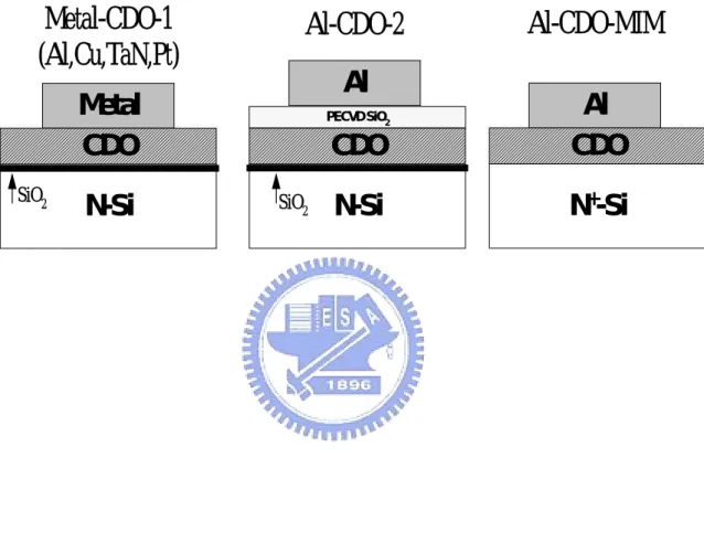
Fig. 3.1 Schematic drawings of the MIS structures used in this work. Metal-CDO-1 : Metal/ CDO (200 nm)/ SiO2 (10 nm)/n-Si. Al-CDO-2 : Al(500 nm)/ PECVD SiO2 (30 nm)/ CDO (200 nm)/ SiO2 (10 nm)/n-Si. Al-COD-MIM : Al (500 nm)/ CDO (200 nm)/n+-Si.
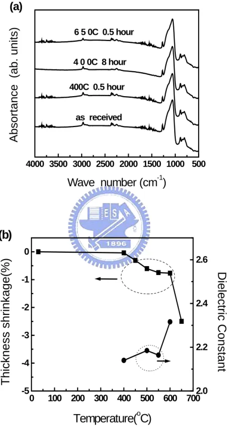
Fig. 3.2 (a) FTIR spectra and (b) thickness shrinkage and dielectric constant variation of CDO film after thermal annealing at different temperatures.
Fig. 3.3 (a) Current density-electric field characteristic of Al-COD-MIM sample measured at different temperatures. (b) The breakdown characteristics of Al-CDO-MIM capacitors at 200°C
Fig. 3.4 Capacitance-voltage curves of Al-CDO-1 sample measured from inversion mode to accumulation mode (FVS) and from accumulation mode to inversion mode (RVS)
Fig. 3.5 Capacitance-voltage curves of Al-CDO-1 sample after electrical stress at -2MV/cm and +2MV/cm fro 4 minutes.
before and after BTS test at +1 MV/cm and 200℃ for 60 min.
Fig. 3.7 SIMS depth profiles of TaN-CDO-1 sample before and after BTS test at +1 MV/cm and 200℃ for 60 min.
Fig. 3.8 SIMS depth profiles of Al-CDO-1 samples after annealing at 400℃ for various time periods.
Fig. 3.9 Capacitance-voltage curves of Al-CDO-2 sample with different voltage ranges and different sweep directions.
Fig. 3.10 Capacitance-voltage curves result of Al-CDO-2 sample after BTS at (a) room temperature and (b) 150°C. The electric field is 0.6MV/cm
Fig. 3.11 Arrhenious plot of the dielectric polarization of CDO film.
Fig. 3.12 C The J-E characteristic of Al-CDO-1 sample can be well fitted by (a) Schottky emission model at low temperature and low electric field and (b) Frenkel-Poole model at high temperature and high electric field.
Fig. 3.13 The J-E characteristic of Al-CDO-2 sample at negative gate voltage can be well fitted by Schottky emission model from room temperature to 200°C. Fig. 3.14 Proposed model to explain the observed electrical instability of
Metal-CDO-1 capacitors.
Fig. 3.15 The cumulative TDDB failure of Al-CDO-1, Cu-CDO-1 and TaN-CDO-1 samples stressed at 1MV/cm, 1MV/cm, and 3.5MV/cm, respectively. The
temperature is 200°C.
Fig. 3.16 Extrapolation of TDDB lifetime of TaN-CDO-1 sample at 200°C according to E-model.
Chapter 4
Fig. 4.1 Schematic structure of Cu-interconnect fabricated by dual-damascene process.
Fig. 4.2 Schematic structures of the MIS capacitors used in this work. Al-SiC-1 : Al (500 nm)/ SiC (90 nm)/ SiO2 (10 nm)/ Si. Cu-SiC-MIM : Cu (500 nm)/ SiC
(90 nm)/n+-Si. Cu-SiC-1 : Cu (500nm)/ SiC (90nm)/ FSG(750nm)/ Si. Cu-FSG-1: Cu (500nm)/ FSG(750nm)/ Si. Al-MIM-1 : Al(500nm)/ SiC (90nm)/ n+-Si. Al-SiO2-1 : Al / SiO2 (10 nm)/ Si
Fig. 4.3 TDS analysis of three different SiC films stored in cleanroom for 2 weeks Fig. 4.4 SIMS depth profiles Cu ions in the three different SiC films after BTS at
+2MV/cm and 200℃ for 500 minutes stress.
Fig. 4.5 (a)Vfb shift value of Cu-SiC-1 and Cu-FSG-1 capacitors after BTS (b) C-V characteristics of the Cu-MIS-1 sample after BTS for various lengths of time. Fig. 4.6 The leakage current and breakdown phenomenon of Cu-SiC-MIM capacitors
Fig. 4.7 The high frequency C-V characteristics of Al-SiC-1 sample measured in both of the FVS and RVS modes for two cycles. The voltage range is –40 to 40 V. Fig. 4.8 Capacitance-voltage curves of Al-SiC-1 samples measured at room
temperature after BTS at 200 ℃ for 3 hours. The electric field strengths are at (a) ±0.4; (b) ±0.5, and (c) ±0.6 MV/cm.
Fig. 4.9 Capacitance-voltage curves of Al-SiC-1 samples measured at room temperature after BTS at (a) 150 and (b) 175 ℃ for 3 hours. The electric field was fixed at ±0.5 MV/cm.
Fig. 4.10 Capacitance-voltage curves of Al-SiC-1 sample after continuous electric field stress. At (a) –20 V (-2 MV/cm) and (b) +20 V (+2 MV/cm). The temperature was fixed at 25 ℃.
Fig. 4.11 Schematic illustration of proposed polarization model for electrical instability of SiC film at high electric field and low temperature.
Fig. 4.12 Extracted dielectric constant of SiC film as a function of frequency with temperature as parameters. Before measurement, Al-SiC-1 samples were biased at –40 V for 2 minutes at room temperature. Results of SiO2 measured from Al-SiO2-1 sample are also shown in the figure.
Fig. 4.13 XPS spectrum of SiC film shows (a) Si(2p) and (b) N(1s) electron binding energy.
Fig. 4.14 Schematic illustration of proposed instability mechanism combining carrier injection and weak polarization to explain electrical instability at low electric field but high temperature.
Fig. 4.15 (a) Current density-electric field (J-E) curve of Al-SiC-1 sample at 30℃. (b) The measured J-E curve at low electric field (<1 MV/cm) can be well fitted by Schottky emission model.
Fig. 4.16 (a) Current density-electric field (J-E) curve of Al-SiC-MIM sample at 30℃. (b) Because of the quasi-symmetric sample structure, the measured J-E curve at all electric field range can be well fitted by Schottky emission model.
Chapter 5
Fig. 5.1 Thermal Desorption Spectroscopy result of SiC outgas
Fig. 5.2. Auger electron spectrum of a partially oxidized SiC film. No carbon content is detected in SiO2 layer.
Fig. 5.3 Fourier-transformed infra-red (FTIR) spectrum of a fully oxidized SiC film. The small C-O peak implies that some carbon remain in SiO2
Fig. 5.4 Oxide thickness versus oxidation time of SiC film oxidized in (a) dry O2 ambient and (b) steam ambient. Steam oxidation is much faster than dry O2 oxidation. Oxidation occurs at temperature as low as 550℃ at acceptable
oxidation rate.
Fig. 5.5 Extraction of oxidation rate constants of SiC in (a) dry O2 ambient and (b) steam ambient. Good linearity indicates that the Deal-Grove model can be used.
Fig. 5.6 Arrhenius plot of parabolic rate constant of SiC oxidation in (a) dry O2 ambient and (b) steam ambient. The activation energy is 0.72eV and 0.55eV in (a) and (b), respectively.
Fig. 5.7 The grown oxide thickness of 54nm thick a-SiC on Si substrate at 600℃ Fig. 5.8 Atomic force microscope surface images of (a) the as-deposited SiC surface,
(b) the partially oxidized and (c) the fully oxidized a-SiC deposited wafer after oxidation and etching of the oxidized layer.
Fig. 5.9(a) the prototypal design of SiC and CDO low-k reclaim instrument with combined vertical furnace and wet chemical bench tank and 6.9(b) final practical instrument model
Chapter 6
Fig. 6.1. (a) IC interconnect high frequency test structure layout (a) Test structure with co-planar structure (b) Test structure without co-planar structure (c) Wafer interconnect stripline cross section
Fig. 6.2. (a)Two port S-parameter measurement network (b) Single conductor interconnect represent model.
Fig. 6.3 P-SiLK co-planar stripline interconnect (a) attenuation and (b) propagation constant versus frequency. The sub-inlet illustration is the Oxide interconnect reference sample.
Fig. 6.4(a) real part and (b) imaginary part of P-SiLK co-planar stripline interconnect characteristic impedance. The sub-inlet illustration is the Oxide interconnect reference sample.
Fig. 6.5 Resistance variation versus frequency from S-parameter measurement of P-SiLK co-planar stripline interconnect
Fig. 6.6 Inductance variation versus frequency from S-parameter measurement of P-SiLK co-planar stripline interconnect
Fig. 6.7 Conductance variation versus frequency from S-parameter measurement of P-SiLK co-planar stripline interconnect
Fig. 6.8 Capacitance variation versus frequency from S-parameter measurement of P-SiLK co-planar stripline interconnect
Fig. 6.9 (a) Extracted loss tangent and (b) metal loss of P-SiLK co-planar stripline interconnect
Chapter 1
Introduction
1.1 General Background
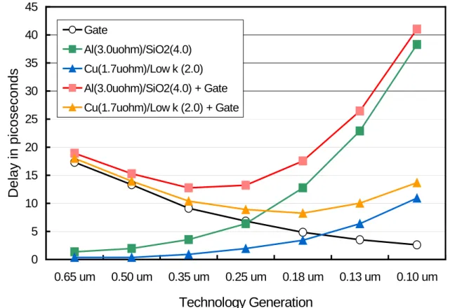
With the progress of microelectronics technology, the semiconductor integrated circuits (ICs) devices area becomes smaller. The Moore’s Law described well that each new generation approximately doubles the device density and increases performance by about 40% while quadruples memory capacity [1]. Currently, ICs designed with 90 nm design rule are being manufactured. The scaling of transistors has necessitated an increase in wiring density to accommodate increasing transistor densities over large chip areas. Generally, the speed of an electrical signal in an IC is governed by two components; one is the switching time of individual transistor, known as transistor gate delay, and the other is the signal propagation time between transistors, known as interconnect resistance-capacitance (RC) delay [2]. However, the Moore’s Law is valid only when RC delay is negligible in comparison with gate delay. Most researches reported that the RC delay would be the dominant factor after 0.25μm technology node. Interconnect parasitic components at 0.18μm technology node begin to dominate not only the overall signal delay, as shown in Fig.1.1, but also
scaling, transistor performance can be improved with reduced gate length, backend interconnection scaling results in higher wire resistance (R) for narrower metal line width and higher inter-/intra-level capacitance (C) for shorter metal line spacing. As a result, a larger portion of the actual circuit speed depends more on the characteristics of interconnects than on the scaling of active devices. The interconnect delay must be reduced by using new materials to alleviate the problem and to achieve higher performance and higher circuit density.
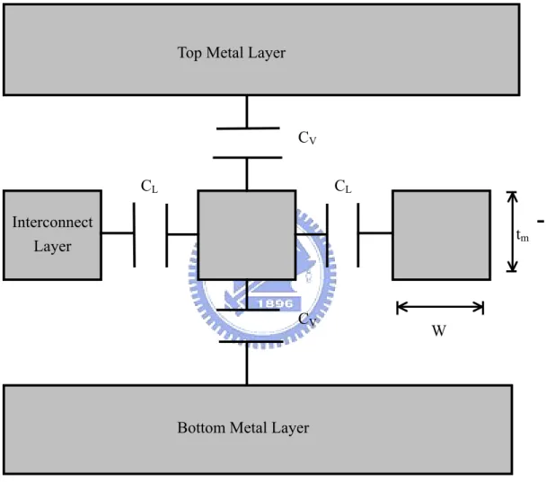
According to a basic interconnect cross-section view shown in Fig. 1.2, assuming that interconnect spacing between continuous interconnect metal lines equals metal line width and the distance between top metal layer and interconnect layer is the same as the interconnect line spacing. In a simple first-order model, the interconnect resistance (R), interconnect capacitance (C), the time delay (RC) and the power consumption (P) of an interconnect system can be expressed as the equations from (1.1) to (1.4), respectively. m m Wt L R= ρ (1.1) ) ( 2 ) ( 2 m m m m V L t W L W t L C C C = + = ε + (1.2) ) ( 2 2 2 2 2 m m m t L W L RC = ρε + (1.3)
,where ρ is the resistivity of metal line, Lm is the metal line length, W is the
interconnect line width, ε is the permittivity of intermetal dielectric, and tm is the
thickness of metal line. In Eq. (1.4), f and V are operation frequency and applied voltage, respectively. According to these equations, it is clear that low-k materials not only lower line-to-line capacitance to reduce the RC delay but also alleviate power dissipation issues [7, 8]. Thus new low-k materials at each level of the interconnect structure (Fig. 1.3) are needed to replace traditional SiO2 to reduce RC delay.
1.2
Multilevel Copper Interconnect Technologies
1.2.1 Cu Metallization
Recently, Cu has been widely accepted as the only solution to replace Al in multilevel interconnect applications [9-14]. Compare to traditional Al and Al alloys, Cu has a lower resistivity of 1.7μΩ-cm with respect to Al alloy of around 3μΩ-cm. Besides, Cu exhibits excellent resistance to electro/stress migration. Cu can be deposited by chemical vapor deposition (CVD) system or electrochemical deposition (ECD) system with great conformity and uniformity at low temperature. Both these two methods supply better step coverage than conventional physical vapor deposition (PVD). In 1997, Cu chips were introduced with SiO2 as intermetal dielectric (IMD)
silicon [16-19]. Thus proper metal/dielectric diffusion barriers are necessary for avoiding Cu ions out diffusion [20-25]. Nowadays, Cu/SiO2 technology is mature. In
order to further optimize ICs performance, new IMD films are required to further reduce RC delay. This perceived need for low-k IMDs in ULSI applications has stimulated great efforts in the development of advanced low-k materials.
1.2.2 Low Dielectric Constant Materials
Although Cu has been successfully integrated with SiO2 in advanced sub-0.25μ
m ICs generation for improved interconnect performance [15]. In order to further improve interconnect RC delay, low-k materials to replace SiO2 are inevitable.
Integration of copper with low-k dielectric can render better ICs performance [26, 27]. Fluorine doped silicon dioxide (FSG) with k~3.6 integrated with Cu was successfully introduced in interconnect system at 0.18μm technology node as the first Cu/low-k interconnect technology. Because that the k value of FSG is not low enough, others lower dielectric films (k = 2.6~3.0) are being studied and introduced for advanced ICs process.
Except the k value, the impact of low-k materials on process integration, manufacture cost, and device reliability must be considered. Lots of low-k materials have been developed recently and are listed in Table 1-1. These materials may be
listed in Table 1-2, and are summarized as follows:
Low dielectric constant with respect to SiO2’s dielectric constant 4.2
Good thermal stability High mechanical Strength Stable Chemical properties Good Electrical characteristics
In order to integrate these low-k materials into advanced interconnect processes; the above requirements are needed for all low-k films.
Some ultra-low-k (ULK) films with relative permittivities lower than 2.2 are generally achieved by the introduction of pore structures. The pore structure would further reduce mechanical strength and thermal conduction, and would increase moisture/chemical adsorption as well [28]. Therefore, all kinds of low-k materials have to meet lots of electrical, mechanical, chemical, and thermal integrity requirements so that interconnect system could deliver the desired electrical performance and ensure device reliability. To fulfill these requirements described above, measurement and evaluation of physical, chemical, thermal, and mechanical properties of low-k and low-k/metal interfaces are urgently required.
integration of Cu and low-k IMD is not easy. Although some leading companies announced mass-production of Cu-interconnect with IMD of k~2.6, most of the Cu chips were fabricated using FSG as IMD since 1997. Low-k materials with k-value lower than 2.2 are not mature.
1.2.2.1 Chemical Vapor Deposition of Low Dieletric Constant Materials
The k-value of SiO2 used as IMD is about 4.1. In order to reduce the dielectric
constant of SiO2 film, incorporating fluorine into SiO2 film is a promising method to
form fluorinated oxide (FSG) with k~3.6. Because of the polarizability of fluorine in thermal oxide for FSG film, k-value of FSG is thus reduced. FSG could be deposited at different deposition process in atmospheric pressure CVD system (APCVD), plasma enhanced CVD system (PECVD), and high-density plasma CVD system (HDPCVD). Except the CVD deposited FSG low-k film, it leaves us different kinds of CVD low-k films listed in Table 1-1 such as diamond like Carbon (k-value 2.8~3.0), Parylene N (k value 2.6~2.8), Polyimide SSQ hybrids (k value 2.7~3), and ultra low-k porous type carbon doped oxide (OrionTM k value 1.8~2.2). Though the
CVD technology is presently used, CVD low-k materials for <65nm technology nodes have not been qualified to date.
1.2.2.2 Spin-On Deposition of Low Dielectric Constant Materials
Spin-on deposited low-k materials are the other candidate for semiconductor fabrication. A liquid state material would firstly deposited on a wafer by spin-coating method. Then a series of thermal treatments must be performed to remove solvent from the as-spun film. Finally, the deposited low-k film is well prepared after a curing step. Table 1-1 lists some spin-on low k films with k-value less then 3 such as poly(arylene ethers), and Cylotenes. Table 1-1 also lists some ultra low-k films with k-value less then 2.4 such as silica aerogels and silica xerogels.
Historically, spin-on materials present an important advantage over CVD materials: the ability to introduce a high degree of porosity in the films (up to 50 percent and more), reaching k values as low as 2.0. But CVD materials can reach similar k-value with lower porosity now. The competition between CVD technique and spin-on technique is expected to exist for several technology nodes.
1.2.2.3 Low Dielectric Constant Diffusion Barrier
Except the low-k IMDs, there is still another important dielectric in Cu dual damascene structure: Cu dielectric diffusion barrier. Barrier materials used for Cu wiring must prevent Cu from diffusion into the adjacent dielectric and must form a suitable, high quality interface with Cu to limit vacancy diffusion and achieve
acceptable electro-migration lifetime. Chemical vapor deposited (CVD) silicon nitride (SiN) and metal nitrides of refractory metals, such as W, Ta, Ti, and etc. are well known Cu ion diffusion barriers. As for dielectric barrier, SiN has been the most favorable candidate. In addition to being used as a barrier layer, SiN has also been used as an etching stop layer (ESL) and a final capping/passivation layer in Cu dual damascene structures. Yet, SiN with its higher dielectric constant (k~7), other new dielectric barriers with lower dielectric constant (such PECVD amorphous silicon carbide, a-SiC) are proposed for advanced Cu interconnect generations.
1.2.3 Concept of Future Interconnect for High Frequency Signal Transmission
Due to the application of low-k IMD and Cu interconnect, the clock rate has reached to RF frequency range, and the conventional lumped circuit R-C model approaches that used to solve hard-wired metal interconnect problems will eventually encounter fundamental limits and may impede the advance of future ULSIs device modeling. We need to find out the more accurately interconnect model of Cu/low k interconnect system at RF frequency. On the other hand, the interconnect performance must be evaluated at RF frequency rather than at relatively low frequency of around MHz. By using scattering parameter (S-parameter) measurement to extracted out the real transmission stripline parameters, resistance, conductance, inductance and
capacitance would help to build up a real interconnect model and this model would help to predict electrical characteristics more accurately.
1.3 Organization of the Thesis
On the basis of the understanding of issues of multilevel interconnect, this thesis focus on the primary topic of Cu and low-k material integration issues, especially try to establish a general physics model to analysis low-k dielectric electrical instability mechanisms. With this physics model, we could apply these analysis steps to all other newly invented low-k films.
This dissertation is divided into seven chapters. The contents of each chapter are described as followed:
In chapter 1, we introduce the background of this dissertation.
In chapter 2, the metal ions diffusion phenomena in FSG with different surface treated metal contact were study. FSG is the most matured and well-known low-k material that has been applied into real ICs and it is would be the most suitable low-k dielectric to study this metal ion caused electrical instability. In real backend Cu dual damascene process, the surface of FSG dielectric would experience different process steps such as dielectric etch, pre-metal deposition sputtering clean, as well as chemical-mechanical polishing. These process steps may change the surface
properties of FSG film. With different metal-dielectric interface conditions, there were different metal ions diffusion levels under electrical stress. Then, a new metal ion diffusion model could be proposed to explain the observed process effect.
In chapter 3, a ultra low k (k < 2.3) dielectric of Carbon-Doped-Oxide (CDO) was evaluated for next generation IC interconnect systems. CDO is a very promising low-k dielectric. The detailed characterization of CDO was performed in this chapter. Besides, the electrical instability mechanisms including metal ions diffusion, dielectric polarization, and carrier injection was discussed in detail. Reliability of CDO was also evaluated.
A newly developed a-SiC was design to replace silicon nitride being a dielectric diffusion barrier in Cu dual damascene structure. Detailed study of a-SiC was performed in Chapter 4. The resistance to Cu diffusion of a-SiC film deposited at different conditions were evaluated at first. Then, the dielectric instabilities due to dielectric polarization and carrier injection was presented and characterized.
In Chapter 5, a new universal method for a-SiC and CDO low-k film reclaim was proposed to replace current chemical and mechanical polishing (CMP) with fast speed, low cost, and low wafer substrate consumption. CDO and a-SiC films can be easily oxidized to SiO2 in oxidant environment at temperature as low as 550℃. The a simple
detail oxidation mechanism and wafer reclaim process as well as the results were presented in the chapter.
In chapter 6, metal/low-k film based co-planar type transmission stripline was used to evaluate the RF performance of the interconnect system. All transmission line parasitic parameters including resistance, inductance, capacitance, and conductance, were extracted from high frequency S-parameters measurements. Both low-k dielectric loss and stripline metallic loss were also extracted and discussed for high frequency application.
In Chapter 7, we summarize all experimental results in this dissertation and suggest some unfinished works and new observed issues for future studies.
References
1 G. E. Moore, “Cramming more components onto integrated circuits”, Electronics, vol. 38, No. 8, pp.114-118, 1965
2. S. P. Jeng, M. C. Chang, and R. H. Havemann, “Process integration and manufacturing issues for high performance interconnect”, MRS Symp. Proc. Adv. Metallization for Devices and circuits, pp.25-30, 1994
3. L. Peters, Semiconductor International, vol. 21, No. 10, pp.64-74, September1998
4. K. Rahmat, O. S Nalagawa, S. Y. Oh, J. Moll, and W. T. Lynch, “A scaling scheme for interconnect in deep-submicron processes”, IEEE International Electron Devices Meeting, pp.245-248, 1995
5. S. Crowder, S. Greco, H. Ng, E. Barth, K. Beyer, g. Biery, J. Connolly, C. Dewan, R. Ferguson, X. Chen, M. Hargrove, E. Nowak, P. McLaughlin, r. Purtell, R. Logan, J. Oberschmidt, A. Ray, D. Ryan, K. Tallman, T. Wagner, V. McGhay, E. Crabbe, P. Agnello, R. goldblatt, L. Su, and B. Davari, “A 0.18 μ m high-performance logic technology ”, Symp. VLSI Tech. Dig. , pp.105-106, 1999 6. R. Hossain, f. Viglione, M. Cavalli, “Designing fast on-chip interconnects for
deep submicrometer technologies”, IEEE Trans. on Very Large Scale Integration (VLSI) systems, vol. 11, No.2, pp.276-280, 2003
7. J. Ida, M. Yoshimaru, T. Usami, A. Ohtomo, K. Shimokawa, A. Kita, M. Ino, “Reduction of wiring capacitance with new low dielectric SiOF interlayer film for high speed/low power sub-half micron CMOS”, IEEE Symp. VLSI Technol. Digest, pp. 59-60, 1994
8. T. Sakurai, “Closed-form expressions for interconnection delay, coupling, and crosstalk in VLSIs”, IEEE Trans. on Electron Devices, vol. 40, No.1, pp.
118-124, 1993.
9. T. Takewaki, R. Kaihara, T. Ohmi, and T. Nitta, “Excellent electro/stress-migration-resistance surface-silicide passivated giant-grain Cu-Mg alloy interconnect technology for giga scale integration (GSI)”, IEEE International Electron Devices Meeting, pp253-256, 1995
10. P. Singer, Semiconductor International, pp. 52-56, November, 1994
11. J. Torres, “Cu dual damascene for advanced metallisation (0.18 µm and beyond)”, IEEE Int. Interconnect Tech. Conf., pp. 253-255, 1999
12. T. Ritzodorf, L. Graham, S. Jin, c. Mu, and D. Fraser, “Self-annealing of electrochemically deposited copper films in advanced interconnect applications ”, IEEE Int. Interconnect Tech. Conf., pp.166-168, 1998
13. C. H. Lee, K. H. Shen, T. K. Ku, c. H. Luo, C. C. Tso, H. W. Chou, and C. Hsia, “CVD Cu technology development for advanced Cu interconnect applications”, IEEE Int. Interconnect Tech. Conf., pp. 242-244, 2000
14. J. Zhang, D. Denning, G. Braeckelmann, R. Venkatraman, R. Fiordalice, and E. Weitzman, “CVD Cu process integration for sub-0.25 µm technologies ” IEEE Int. Interconnect Tech. Conf., pp.163-165, 1998
15. D. Edelstein, J. Heidenreich, R. Goldblatt, W. Cote, C. Uzoh, N. Lustig, P. Roper, T. McDevitt, W. Motsiff, J. Dukovic, R. Wachnik, H. Rathore, R. Schultz, L. Su, S. Luce, and J. Slattery, “Full Copper Wiring in a Sub-0.25um CMOS VLSI Technology”, International Electron Devices Meeting, pp.773-776, 1997
16. 15. S. M. Sze, Physics of Semiconductor Devices, 2nd ed. New York: John Wiley & Sons, Chap. 6-8, 1981,
16. A. Cros, and K. N. Tu, “Formation, Oxidation, Electronic, and Electrical Properties of Copper Silicides”, J. Applied Physics, vol. 67, No. 7, pp.
3328-3336, 1990
17. L. Stolt and F. D’Heurle, “The Formation of Cu3Si: Marker Experiments”,Thin Solid Films, vol. 189, No.2, pp. 269-274, 1990
18. J. Echigoya, H. Enoki, T. Satoh, T. Waki, M. Otsuki, and T. Shibata, “Thin Film Reaction and Interface Structure of Cu on Si”, Applied Surface Science, vol. 56-58, Part 1, pp 463-468, 1992
19. T. H. Lee, “Nitridation Effect on the Barrier Property of Mo and Cr Layer in Cu/Barrier/SiO2/Si MOS Structures”, Master Thesis, National Chiao-Tung
University, Hsinch, Taiwan, 1997
20. Y. C. Lin, “Barrier Property of W-Silicide and Ta-Nitride for Cu Metallization”, Master Thesis, National Chiao-Tung University, Hsinch, Taiwan, 1997
21. Y. S. Diamand, A. Dedhia, d. Hoffstetter, and W. G. Oldham, “Copper Transport in Thermal oxide”, J. Electrochem. Soc., vol. 140, No. 8, pp. 2427-2432, 1993 22. A. L. S. Loke, C. Ryu, C. P. Yue, J. S. H. Cho, and S. S. wong, “Kinetics of
copper drift in PECVD dielectrics”, IEEE Electron Device Letters, vol. EDL-17, pp.549-551, Dec. 1996
23. D. Gupta, “Comparative Cu Diffusion Studies in Advanced Metallizations of Cu and Al-Cu Based Thin Films”, Materials Research Society Symposium Proceedings, vol. 337, pp. 209-215, 1994
24. J. D. Mcbrayer, R. M. Swanson, and T. W. Sigmon, “ Diffusion of Metals in Silicon Oxide”J. Electrochem. Soc., vol. 133, No. 6, pp-1242-1246, 1986
25 X. W. Lin and D. Pramanik, “Future interconnect technologies and copper metallization”, Solid State Technol., pp. 3-79, Oct. 1998
26. The International Technology Roadmap for Semiconductors, Section: Interconnect, 2003
27. K. Maex and G. Groeseneken, “Why we need to rethink copper low-k reliability issues”, Solid State Technology, vol. 46, No.1, pp.30-31, 2003
28. The International Technology Roadmap for Semiconductors, Section: Interconnect, 1997
Table 1-1 Summary of promising low-k candidates
Materials K value depostion method
Polymides 3.0-3.6 spin on
Spin-on Glasses 2.7-3.1 spin on
Fluorinated Polymides 2.6-2.9 spin on DLC (Diamond like Carbon) 2.8-3.0 CVD Poly(arylene ethers) 2.6-2.9 spin on
Poly(arylenes) 2.6-2.8 spin on Cylotenes 2.6-2.8 spin on Parylene N 2.6-2.8 CVD Poly(norbornenes) 2.5-2.7 spin on Polyimide SSQ hybrids 2.7-3.0 CVD Alkyl-silanes/N2O 2.4-2.7 spin on Ultra-low K Teflon-AF 1.9-2.1 spin on
Teflon microemulsion 1.9-2.1 spin on
Orion 1.8-2.2 CVD
Polymide nanofoams 2.2 spin on
Silica aerogels 1.1-2.2 spin on
Silica xerogels 1.5-2.2 spin on
Table 1-2 Basic requirements for low dielectric constant materials
Thermal Properties Mechanical Strength Chemical Properties Electrical Characteristic Thermal stability Thickness uniformity Solvent, acids, PR
strippers resistance
Isotropic and stable dielectric constant Glass transition
temperature
Adhesion No corrosion to metal Electrical strength
Thermal shrinkage: thickness, weight loss,
stress hysteresis
Stress Moisture adsorption Breakdown field
Outgassing Tensile Modulus, tensile strength
Purity TDDB life-time, activation energy Thermal expansion
coefficient
Strain Storage life Leakage
Thermal conductivity Hardness, density Gas permeability Charge Crack resistance Environmental, safety,
and health
Thickness=0.8um, Length=43um
Source : SIARoadmap-1997
0 5 10 15 20 25 30 35 40 45 0.65 um 0.50 um 0.35 um 0.25 um 0.18 um 0.13 um 0.10 um Technology Generation Delay in picoseconds Gate Al(3.0uohm)/SiO2(4.0) Cu(1.7uohm)/Low k (2.0) Al(3.0uohm)/SiO2(4.0) + Gate Cu(1.7uohm)/Low k (2.0) + Gate
Fig. 1.2 Cross-section of interconnect system showing parasitic capacitance. Interconnect Layer tm W CV CL CV CL
Bottom Metal Layer Top Metal Layer
Chapter 2
Surface-Processing-Enhanced Copper Diffusion
into Fluorosilicate Glass
2.1 Introduction
As mentioned in chapter-1, it is well accepted that copper (Cu) and low dielectric constant (low-k) materials are inevitable at the sub-0.13 micron technology nodes [1,2]. Because Cu is a serious contamination source in silicon and most of the dielectrics, Cu lines must be sealed with suitable diffusion barriers in Cu dual damascene scheme, and Cu contamination during processing must be monitored and controlled [3-6]. Therefore, the meaning of understanding the mechanism of Cu diffusion into the dielectric is twofold. First, if the dielectric shows a good barrier property, diffusion barrier layers can be eliminated. The process can be simplified and the performance can be further improved. Second, if Cu can diffuse into the dielectric, the diffusion behavior must be understood such that contamination during processing can be monitored and controlled.
Many low-k materials have been proposed in the past ten years to reduce interconnect capacitance. Among them, the fluorosilicate glass (FSG) is the most desirable because of its good thermal and chemical stability and its similarity to
silicon dioxide (SiO2). Hence it can be readily integrated into the fabrication process
[7-10]. Recently, Cu and FSG had been successfully integrated together and became standard process [11-13]. However, only a few articles in the literature examined the diffusion behavior of Cu into FSG film [14-18]. Furthermore, quite different results were reported in those articles. It was even reported that Cu does not diffuse into FSG film under the bias-temperature stress (BTS) at 200 ℃ and 3.5 MV/cm for 30 minutes[17].
The major drawback of the previous studies is that they all used as-deposited FSG film to examine the behavior of Cu diffusion in FSG film. This is not appropriate for the following reasons. In the damascene process, FSG film would experience several processes, such as dielectric etching, ion-sputtering clean before metal deposition, and chemical-mechanical polish (CMP) [19]. Fig.2.1 describes the major steps of Cu dual-damascene process. After the first Cu-interconnect layer is finished, inter-metal-dielectric (IMD) Cu-interconnect is deposited as the next layer (Fig.2.1(a)). The sequential photo-lithography process and dielectric etch processes are performed twice to form the via holes and trenches in the IMD (Fig.2.1(b)). After pre-metal deposition cleaning, barrier metal and Cu are then deposited into the via holes and trenches followed by a CMP process to finish the second layer Cu-interconnect (Fig.2.1(c)). Although the CMP process is employed to remove the Cu and barrier
metal, the surface of FSG film is also polished during the over polishing period. It is the behavior of the Cu diffusion into processed FSG film that affects the integration scheme and the contamination control. Therefore, it is important to examine the effects of surface processing on the Cu/FSG interface reaction and the diffusion behavior of Cu into FSG film, which is the focus of this chapter. Realizing this dual damascene process induced effects would be helpful to realize all other low-k films’ behaviors in a damascene structure.
2.2 Experimental Details
Simple metal-insulator-silicon (MIS) capacitor structures were used. The starting material is an (100)-oriented p-type silicon wafer. A 10 nm thick oxide was thermally grown before the FSG deposition to minimize the dielectric/silicon interface state density. FSG film of about 750 nm thickness was deposited in a high-density plasma chemical vapor deposition (HDPCVD) system. An inductively coupled plasma (ICP) source was used to generate plasma. The frequency and power of the radio-frequency (RF) generator for the top electrode were 200 MHz and 350 W, respectively. The RF power of the bottom electrode was turned-off such that no ion bombardment occurred during deposition. It should be noted that substrate bias is not necessary for the damascene process because IMD is deposited on a CMP planarized
flat surface. The gases and corresponded flow rates were SiH4(17 sccm), SiF4(96
sccm), O2(190 sccm), and Ar(125 sccm). The chamber pressure was 15 mTorr during
deposition.
Wafers were then divided into three categories: without surface processing (the as-deposited sample), argon ion sputtering in an ICP chamber for 1 minute (the ICP sample), and CMP partial polish (the CMP sample). The ICP chamber is the pre-treatment chamber of a clustered metal deposition system. Both of the top and bottom powers were set at 300 W. This is the typical surface sputtering condition before metal deposition. The sputter rate of FSG film at this condition is about 200 nm/min. The CMP partial polish is to simulate the damage that arises during the over-polish period of the Cu CMP process. Clean pad and fresh slurry of Model ECC-1403-1 were used to avoid Cu contamination from pad or slurry. The pad pressure was set at 2 Psi and the polishing time is 50 sec. The thickness of the FSG film was reduced by 200 nm after the ICP process and by 50 nm after the CMP process. Copper film of 500 nm thickness was then deposited in an ionized metal plasma (IMP) chamber without substrate bias. Gate electrodes were then patterned by the wet process. Samples with Al gate were also prepared as reference. The Al film was deposited in a typical high vacuum DC sputter system.
passivate the MIS structure. This layer is used to avoid moisture absorption in the MIS structure and to prevent the Cu gate from oxidation during high temperature measurement. A 30 minutes annealing in N2 ambient at 300 ℃, to reduce the
process-induced charges in the dielectrics, finalized the sample processing. The temperature of this step is generally at 400℃, but in our experiment it is reduced to 300℃ to avoid Cu diffusion into the FSG during annealing. Table 2-1 summarizes the process condition of the 6 samples.
The total dielectric thickness of each sample was measured by optical interference method. The high frequency capacitance-voltage (HFCV) characteristics of all of the samples were measured at 100KHz. The dielectric constant of each sample was calculated from the measured capacitance at the accumulation mode and the total dielectric thickness was again determined by optical method. The flat-band voltage (Vfb) was also extracted from the HFCV characteristic.
A bias-temperature stress (BTS) at +1MV/cm and 200℃ was performed to drive Cu into the FSG film. Secondary-ion-mass-spectroscopy (SIMS) was employed to determine the distribution of Cu in the FSG film. To avoid surface roughness and knock-on effect during SIMS analysis, the capping SiN was removed by CF4 plasma,
and the metal gate was selectively removed by warm HNO3 before SIMS analysis.
Spectroscopy (TDS) were also used to analyze the properties of the surface processed FSG film.
2.3 Metal Ion Diffusion in Surface Processed FSG
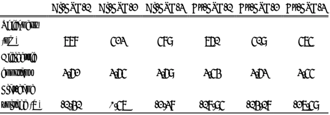
The fluorine concentration of the deposited FSG film determined by FTIR is about 4.6 %. Table 2-2 lists the dielectric thickness, effective dielectric constant, and flat-band voltage of the six samples. Although ICP and CMP treatments reduced the film thickness, the dielectric constant is unchanged. These results imply that the two surface processes did not change the composition and structure of the bulk of the FSG film. The magnitudes of Vfb of Al-gate devices are small. The slight difference
between the samples may be due to surface process induced damages or the fixed charges in the deposited FSG film.
An obvious Vfb shift toward the negative voltage axis is observed for the
Cu-gate devices. One obvious hypothesis to explain this observation is Cu contamination during the Cu deposition or thermal processes. Fig.2.2 shows the SIMS depth profiles of Cu in the FSG film of the Cu-FSG-1 and Cu-FSG-3 samples. Depth profiles of the Cu-FSG-1 sample and the Cu-FSG-3 sample are almost identical, and only a small amount of Cu atoms were detected at the surface. These results indicated that the trace amount of Cu atoms comes from the residual Cu at the FSG surface after
the stripping of the Cu gate. The concentration of typical mobile ions, such as Na+ and
K+, were below the detection limit of SIMS analysis. Therefore, the negative V
fb is
explained by the residual fixed charges in the FSG film generated during Cu deposition [20]. These charges are immobile and will not change at temperatures lower than the final annealing temperature of 300℃.
To drive Cu into FSG film, BTS tests were performed at +1 MV/cm and 200 ℃ for various periods. To exclude the possible instability of the FSG film itself and contamination during the surface processing, Al-gate MIS capacitors were also measured. The flat-band voltage shift (∆Vfb) of the Al gate and the Cu gate samples
after BTS were extracted and were denoted as ∆Vfb,Al and ∆Vfb,Cu, respectively. The
∆Vfb relevant to Cu was then corrected by subtracting ∆Vfb,Al from ∆Vfb,Cu. Fig.2.3
shows the corrected ∆Vfb of the three Cu-gate samples after various BTS periods. The
∆Vfb,Al of the Al-FSG-1, Al-FSG-2, and Al-FSG-3 samples are also shown in Fig.2.3.
A slightly positive shift of Vfb was observed on all of the three Al-gate samples, but
the magnitudes of ∆Vfb,Al of the three samples were similar. This phenomenon is
attributed to the slight instability of the FSG film itself [18?]. A net negative ∆Vfb was
observed on all of the three Cu-gate samples. Since the flat-band voltage shift due to the instability of the FSG film and contamination other than Cu after the surface treatment had been subtracted, the ∆Vfb should be relative to the Cu only. It is obvious
that the ICP sample (Cu-FSG-3) had the largest ∆Vfb and the as-deposited sample
(Cu-FSG-1) had the least ∆Vfb. Furthermore, the rates of the Vfb shift of the three Cu
gate samples are Cu-FSG-3, Cu-FSG-2, and Cu-FSG-1 in the sequence from high to low. These phenomena imply that Cu is more easily driven into surface processed FSG films than driven into un-processed FSG film. Since the ICP sputtered sample (Cu-FSG-3) shows the most severe Cu diffusion, the following discussion and analysis will focus on the Cu-FSG-3 sample, with the Cu-FSG-1 sample as reference.
Fig.2.4 shows the SIMS depth profiles of Cu in the FSG film of the Cu-FSG-1 and Cu-FSG-3 samples before and after BTS for 30 minutes. Apparent Cu diffusion into the FSG film to a depth of about 40 nm was observed from the Cu-FSG-3 sample after BTS. According to the SIMS analysis, it is definitely confirmed that the ∆Vfb
observed after BTS is due to Cu diffusion into the FSG. The amount of Cu in the FSG film of the Cu-FSG-1 sample after BTS is much lower than that of the Cu-FSG-3 sample after BTS. This is consistent with the trend of Vfb shown in Fig.2.2. Because
the diffusion behavior of Cu in all FSG films should be of the same in the deep inside of FSG films, the only difference among the FSG films is the surface characteristic for Cu diffusion through the Cu/FSG interface. It is thus suspected that the surface processing either increases the Cu ionization rate or reduces the diffusion barrier height and then enhances the Cu diffusion into the FSG film.
FTIR analysis was performed to clarify the FSG property after the surface processing. The transmitted absorption spectrum was detected and the spectra of as-deposited and surface processed FSG films are identical. This confirms the previous postulation based on the dielectric constant and the SIMS profile of Cu that surface processes only modify the properties of the surface layer of FSG film. Fig.2.5(a) and (b) show the H2O and HF desorption spectra analyzed by TDS,
respectively, of as-deposited FSG film, FSG film at 4 days after deposition, and FSG film at 3 days after ICP sputtering. The surface sputtered FSG film shows the strongest H2O desorption signal. This indicates that the surface sputtering enhances
the moisture absorption of the FSG surface layer. It is also observed from Fig.2.5(b) that HF desorption of the ICP sputtered FSG film is more serious than that of the as-deposited FSG film. The controversial result that FTIR does not detect differences between as-deposited FSG film and ICP sputtered FSG film may be attributed to the weak sensitivity of transmitted FTIR on the surface layer property change. In our experience, moisture uptake of as-deposited FSG film cannot be detected by FTIR until 2weeks after deposition.
It has been reported that FSG film with a higher fluorine concentration has a lower dielectric constant, but becomes more easily hygroscopic [21, 22]. The FSG film after moisture absorption will induce a hydrolysis reaction, which is represented
by the following chemical formula [21-23] : ─Si─F + H2O ─> ─Si-OH + HF
The results obtained indicate that all FSG films have a probability of hydrolysis reaction occurrence for the Si─F bonds. The increase in the amount of Si─OH bonds slightly increases the dielectric constant for their low polarity. Moreover, the hydro-fluorine (HF) generated from Si─F bonds would damage other contacted films. Referring to the TDS result, it is postulated that the surface processing produces a surface damage layer. The enhanced moisture absorption at the surface damaged layer causes increased hydrolysis reactions. There can be more Si-OH bonds and HF generation to enhance the copper ionization and erosion rate, and thus more copper ions are generated. This effect, combined with the structural damage due to the CMP and ion sputtering, caused the barrier height for Cu penetration into FSG to roll off and more Cu ions to be driven into FSG under the same BTS condition. Since the FSG film is very thick, it is possible that the increase of the dielectric constant at the surface damaged layer does not affect the effective dielectric constant of the whole film.
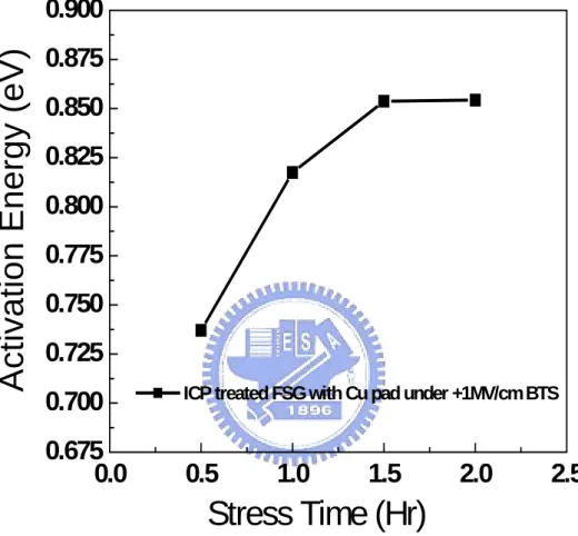
Fig.2.6 plots the activation energy of Cu-FSG-3 sample for Cu mobile ions drift in FSG under BTS stress from Cu-FSG-3 samples. It is observed that with longer stress time, larger Cu drift activation energy is needed for Cu ions into FSG bulk
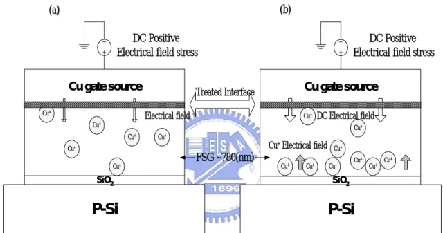
dielectric. It became harder for Cu ions to be driven into FSG films. It is believed that Cu ions which drift into bulk FSG film would finally accumulate at FSG/Si-substrate surface. Fig.2.7 explains the Cu ions behavior model. With initial BTS condition (Fig.2.7 (a)), Cu ions were easily drifted into bulk FSG under high electric field (E-field). Some Cu ions would finally reach and stop at the FSG/Si interface with the large amount of positive Cu ions being driven into FSG. Thus a reverse positive E-field would formed and then even reduced the FSG internal E-field biased from Cu metal gate voltage as shown in Fig.2.7(b).
2.4 Summary
Our investigation discovered that surface processing enhances Cu ion diffusion into FSG film. A surface-damage-layer-enhanced Cu ionization model was proposed. According to the model, the moisture uptake ability of the FSG film greatly affects the Cu diffusion behavior. This may explain the inconsistent reports in the published literature. Furthermore, even if the as-deposited FSG film shows good barrier properties against Cu diffusion, the damascene process will produce a surface damage layer to enhance the Cu diffusion. Thus, in the Cu/FSG integration process, the processed FSG surface must be isolated from any Cu contamination. Therefore, a suitable barrier layer is still necessary because the FSG film has been processed
processed film, instead of as-deposited film, be used to evaluate the behavior of Cu diffusion into all of the low k dielectric films.
References
1. R. J. Gutmann, “Advanced silicon IC interconnect technology and design: Present trends and RF wireless implications”, IEEE Transactions on Microwave Theory and Technique, vol. 47, No. 6, pp.667- 764, 1999
2. N. Awaya, H. Inokawa, E. Yamamoto, Y. Okazaki, M. Miyake, Y. Arita, and T. Kobayashi, “Evaluation of a copper metallization process and the electrical characteristics of copper-interconnected quarter-micron CMOS”, IEEE Transactions on Electron Devices, vol. 43, No. 8, pp. 1206-1212, 1996
3. J. D. McBrayer, R. M. Swanson, and T. W. Sigmon, “Diffusion of Metals in Silicon Oxide”, J. Electrochem. Soc., vol. 133, No. 7, pp. 1242-1246, 1986 4. S. P. Murarka, R. J. Gutmann, A. E. Kaloyeros, and W. A. Lanford, “Advanced
Multilayer Metallization Schemes with Copper Interconnection Metal”, Thin Solid Film, vol. 236, No. 1-2, pp. 257-266, 1993.
5. D. Gupta, “Diffusion in several materials relevant to Cu interconnection technology”, Materials Chemistry and Physics, vol. 41, No. 3, pp.199-205, 1995. 6. A. S. Loke, J. T. Wetzel, P. H. Townsend, T. Tanabe, R. N. Vrtis, P. Zussman, D.
Kumar, C. Ryu, and S. S. Wong, “Kinetics of copper drift in low-kappa polymer interlevel dielectrics”, IEEE Transactions on Electron Devices, vol. 46, No. 11, pp. 2178-2187, 1999
7. T. Homma, R. Yamaguchi, and Y. Murao., “A Room Temperature Chemical Vapor Deposition SiOF Film Formation Technology for the Interlayer in Submicron Multilevel Interconnectrions”, Journal Electrochemical Society, vol. 140, No.3, pp. 687-692, 1993
8. M. K. Bhan, J. Huang, and D. Cheung, “Deposition of stable, low k and high deposition rate SiF4-doped TEOS fluorinated silicon dioxide (SiOF) films”, Thin
Solid Films, vol. 308-309, pp.507-511, 1997
9. C. O. Jung, K. K. Chi, B. G. Hwang, J. T. Moon, M. Y. Lee, and J. G. Lee, “Advanced plasma technology in microelectronics”, Thin Solid Films, vol. 341, No. 1-2, pp.112-119, 1999
10. S. P. Kim, and S. K. Choi, “The origin of intrinsic stress and its relaxation for SiOF thin films deposited by electron cyclotron resonance plasma-enhanced chemical vapor deposition”, Thin Solid Films, vol. 379, No. 1-2, pp. 259-264, 2000
11. E. P. Barth, T. H. Ivers, P. S. Mlaughlin, A. Mcdonald, E. N. Levine, S. E. Greco, J. Fitzsimmons, I. Melville, T. Spooner, C. DeWan, X. Chen, D. Manger, H. Nye, V. McGahay, G. A. Biery, R. D. Goldblatt, and T. C. Chen, “Integration of copper and fluorosilicate glass for 0.18 µm interconnections”, IEEE Int. Interconnect Technol. Conf., pp. 219-221, 2000
12. R.D. Goldblatt, B. Agarwala, M.B.Anand, E. P. Barth, G. A. Biery, Z. G. Chen, S. Cohen, J. B. Connolly, A. Cowley, T. Dalton, S. K. Das, C. R. Davis, A. Deutsch, C. DeWan, D. C. Edelstein, P. A. Emmi,C. G. Faltermeier, J. A. Fitzsimmons, J. Hedrick, J. E. Heidenreich, C. K. Hu, J. P. Hummel, P. Jones, E. Kaltalioglu, B. E. Kastenmeier, M. Krishnan, W. F. Landers, E. Liniger, J. Liu, N. E. Lustin, S. Malhotra, D. K. Manger, V. McGahay, R. Mih, H. A. Nye, S. Purushothaman, H. A. Rathore, S. C. Seo, T. M. Shaw, A. H. Simon, T. A. Spooner, M. Stetter, R. A. Wachnik, and J. G. Ryan, “A high performance 0.13 µm copper BEOL technology with low-k dielectric ”, IEEE Int. Interconnect Technol. Conf., pp. 261-262, 2000
13. S. S. Lin, C. W. Chen, S. M. Huang, T. K. Kang, C. N. Yeh, T. L. Li, B. Y. Tsui, and C. C. Hsia., “An optimized integration scheme for 0.13 µm technology node
dual-damascene Cu interconnect”, IEEE Int. Interconnect Technol. Conf., pp. 273-275, 2000
14. K. Mikagi, H. Ishikawa, T. Usami, M. Suzuki, K. Inoue, N. Oda, S. Chikaki, I. Sakai, and T. Kikkawa, “Barrier metal free copper damascene interconnection technology using atmospheric copper reflow and nitrogen doping in SiOF film”, IEEE Int. Electron Devices Meeting, pp.365-368.1996
15. C.S. Pai, A. N. Velaga, W. S. Lindenberger, W. Y.-C. Lai, K. P. Cheung, “Highly reliable low-ϵ (3.3) SiOF HDP-CVD for subquarter-micron CMOS applications”, IEEE Int. Interconnect Technol. Conf., pp. 42-44, 1998
16. G. Passemard, P. Fugier, P. Noel, F. Pires, and O. Demolliens, “Study of fluorine stability in fluoro-silicate glass and effects on dielectric properties”, Microelectronic Engineering, vol. 33, No. 1-4, pp. 335-342, 1997
17. A. Labjadh, F. Braud, J. Torres, J. Palleau, G. Passemard, F. Pires, J. C. Dupuy, C. Dubois, and B. Gautier., “Study of the thermal stability at the Cu/SiOF interface”, Microelectronics Engineering, vol. 33, No. 1-4, pp. 369-375, 1997
18. A. Abdul-Hak, C. Ahrens, W. Hasse, and J. Ullmann, “Investigation of copper diffusion in SiOF, TEOS oxide and TCA oxide using bias thermal stress (BTS) tests”, Microelectronic Engineering, vol. 37-38, No. 1-4, pp. 205-210, 1997 19. S.Wolf, and R. N. Tauber, Silicon Processing for the VLSI ERA Volume1, 2nd.,
Lattice Press, California, 2000
20. T. P. Ma and P. V. Dressendorfer, “Ionizing Radiation Effects in MOS & Circuits”, John Wiley & Sons, New York, pp. 374-374,1989..
21. S. Lee, and J. W. Park, “Effect of fluorine on moisture absorption and dielectric properties of SiOF films”, Materials Chemistry and Physics, vol. 53, No. 2, pp.150-154, 1998
22. M. Yoshimaru, S. Koizumi, K. Shimokawa, and J. Ida, “Interaction between water and fluorine-doped silicon oxide film deposited by PECVD”,Proceedings of IEEE Int. Reliability Physics Symposium, pp.234-241, 1997
23. T. Homma, “Instability of Si-F bondss in fluorinated silicon oxide (SiOF) films formed by various techniques”, Thin Solid Films, vol. 278, No. 1-2, pp. 28-31, 1996
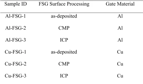
Table 2-1 Process conditions of samples used in this work. Sample ID FSG Surface Processing Gate Material
Al-FSG-1 as-deposited Al Al-FSG-2 CMP Al Al-FSG-3 ICP Al Cu-FSG-1 as-deposited Cu Cu-FSG-2 CMP Cu Cu-FSG-3 ICP Cu
Table 2-2 Dielectric thickness, effective dielectric constant, and flat-band voltage of all of the six samples.
Al-FSG-1 Al-FSG-2 Al-FSG-3 Cu-FSG-1 Cu-FSG-2 Cu-FSG-3 Thickness (nm) 788 523 589 761 519 575 Dielectric constant 3.62 3.65 3.69 3.54 3.63 3.55 Flat-band voltage (V) -1.41 0.57 -2.38 -18.95 -14.18 -27.59
(c) (b) (a) Cu Barrier SiN IMD • SiN deposition • IMD deposition • via patterning • trench • barrier metal deposition • Cu deposition
Fig. 2.1 The major process steps of the dual-damascene process: (a) after IMD deposition, (b) after dual-damascene patterning, and (c) after Cu CMP
10 100 1000 10000 0 20 40 60 80 Depth (nm) Counts/second 100 Cu-FSG-1 before BTS Cu-FSG-3 before BTS
Fig. 2.2 The SIMS depth profiles of Cu in FSG film of Cu-FSG-1 and Cu-FSG-3 samples just after sample preparation. The capping SiN and Cu-gate have been removed