國 立 交 通 大 學
電子工程學系 電子研究所碩士班
碩 士 論 文
高壓製程之靜電放電防護設計
Study of Electrostatistic Discharge
Protection Design in High-Voltage BCD
Processes
研 究 生: 戴嘉岑 (Chia-Tsen Dai)
指導教授: 柯明道教授 (Prof. Ming-Dou Ker)
高壓製程之靜電放電防護設計
Study of Electrostatistic Discharge Protection Design
in High-Voltage BCD Processes
研 究 生:戴嘉岑
Student: Chia-Tsen Dai
指導教授:柯明道教授
Advisor: Prof. Ming-Dou Ker
國立交通大學
電子工程學系
電子研究所
碩士論文
A Thesis
Submitted to Department of Electronics Engineering and Institute of
Electronics College of Electrical and Computer Engineering
National Chiao-Tung University
in Partial Fulfillment of the Requirements
for the Degree of
Master
in
Electronics Engineering
September 2012
Hsinchu, Taiwan
中華民國一○一年九月
高壓製程之靜電放電防護設計
學生: 戴嘉岑 指導教授: 柯明道教授
國立交通大學
電子工程學系 電子研究所碩士班
Abstract (Chinese)
隨著系統電源應用和管理裝置與 IC 產業的緊密結合,高壓金氧半場效應電 晶體(HV MOSFET)已經廣泛運用在 4C 產品(電腦、消費性、通訊、和車用電子 產品),例如電源管理晶片、背光模組控制晶片、觸碰螢幕控制晶片與車用安全 控制晶片等等。在高壓製程中,元件製作程序和相關製程參數較一般低壓製程 來得複雜許多,使得元件製作和確保可靠度上更加困難,高壓元件的結構與傳 統低壓元件相比,必須增加多道淡摻雜層及更為複雜的佈局法則,才能製作出 高壓元件使其能操作在高於數十伏特或者更高的電壓。然而元件之靜電放電防 護能力卻也因此受到製程程序和參數複雜的影響,使得寄生元件導通和排放靜 電放電能量之能力下降。相比傳統低壓製程元件之下,高壓製程元件雖然能承 受高操作電壓,但在靜電轟擊下卻難以有良好之靜電放電防護能力,但隨著市 場需求量日與劇增且急需注意靜電放電防護可靠度之下,此情況開始受到高度 重視,因此如何設計最佳化的高壓靜電放電防護元件,是本篇論文的探討重點。 在 本 篇 論 文 中 , 靜 電 放 電 防 護 元 件 已 被 分 別 實 現 於 162-nm 16-V double-diffused drain MOS (DDDMOS) 製程和 0.25-μm 60-V bipolar CMOS DMOS (BCD) 製程,並分成三個主題探討量測結果,第一部分為探討傳輸線系 統 (TLP system) 量測之脈衝密度 (pulse density) 的影響,由量測結果發現,傳統閘極驅動之靜電放電防護箝制電路 (gate-driven ESD clamp circuit) 由傳輸線 系統量測之二次崩潰電流 (secondary breakdown current, It2) 與經由模擬人體放 電模式 (human body model, HBM) 機台所測得之防護等級在等效耐受能力上有 所差距,而其原因在本實驗中已被確認是由傳輸線系統之脈衝密度所造成,因 此傳輸線系統之脈衝密度在量測高壓製程之靜電放電防護元件時,必須要慎重 考慮。第二部分為探討高壓金氧半電晶體之安全操作範圍 (safe operating area, SOA),為了節省佈局面積,會期望設計出具有良好靜電放電防護能力和寬廣之 安全操作範圍之高壓金氧半電晶體。本部分即針對高壓金氧半電晶體元件結構 進行調查,而實驗數據顯示,藉由適當調整高壓金氧半電晶體元件結構參數, 在維持寬廣安全操作範圍下,能些微提升靜電放電防護耐受度。由於高壓金氧 半電晶體之自我靜電放電防護能力提升有限,因此在第三部分提出靜電放電防 護電路,用以保護內部電路之高壓元件。量測結果顯示,使用閘極驅動技術 (gate-driven technique)、自我基體觸發技術 (self-substrate-triggered technique) 之 防護電路能具有良好之靜電放電防護耐受度。但由於其持有電壓 (holding voltage, Vhold) 低於工作電壓 (VCC),將可能導致栓鎖效應 (latch-up) 的發生,
為了避免栓鎖效應,後續可朝著提高單ㄧ高壓元件之持有電壓並採堆疊元件 (Stacked configuration) 的方式幫助提高防護電路之持有電壓。
Study of Electrostatistic Discharge Protection Design
in High-Voltage BCD Processes
Student: Chia-Tsen Dai
Advisor: Prof. Ming-Dou Ker
Department of Electronics Engineering &Institute of Electronics
College of Electrical and Computer Engineering
National Chiao-Tung University
Abstract (English)
Nowadays, the smart power technology has been developed and used to fabricate the display driver circuits, power switch, motor control systems, and so on. However, the process complexity and the reliability of high-voltage (HV) devices have become more challenging compared with the low-voltage (LV) devices. Among the various reliability specifications, on-chip electrostatic discharge (ESD) protection has been known as one of the important issues in HV integrated circuits (ICs). ESD is an inevitable event during fabrication, packaging and testing processes of integrated circuits. ESD protection design is therefore necessary to protect ICs from being damaged by ESD stress energies.
In this thesis, the ESD protection circuits have been fabricated in 162-nm 16-V double diffused drain MOS (DDDMOS) process and 0.25-μm 60-V bipolar CMOS DMOS (BCD) process respectively. The experimental results and discussions are divided into three parts with different topics in ESD protection design. In part 1, the
influence of pulse density in TLP measurement has been found. In the experimental results, the traditional gate-driven ESD clamp circuit has different secondary breakdown current levels (It2) when using different pulse density. Thus, in order to get a reasonable TLP It2 result, the pulse density should be taken into consideration, especially in HV processes. In part 2, the safe operating area (SOA) of HV MOSFET is studied. To minimize the layout area, it is preferable for HV MOSFET to have high ESD robustness and wide SOA simultaneously without any additional ESD protection circuits in HV ICs. In this work, the self-protected HV MOSFET is investigated with different device structures. According to the experimental results, the ESD robustness of HV MOSFET with modified device structure can be improved slightly under wide SOA. Therefore, to protect the internal HV devices against ESD stresses effectively, the extra ESD protection circuits should be additionally added outside the internal circuits. In part 3, the ESD protection circuits are proposed. Based on the experimental results, the proposed ESD protection circuits with gate-driven technique and self-substrate-triggered technique can have good ESD robustness. However, the holding voltage (Vhold) of the proposed ESD protection
circuits is smaller than the power supply voltage (VCC). Such an ESD element used in the ESD protection circuit may be mistriggered to cause a latch-up failure. To overcome the latch-up issue, the stacked configuration and engineering the holding voltage of each ESD element will be a direction for further study.
Acknowledgements
致謝
首先要感謝的是我的指導教授 柯明道老師,在這碩士兩年紮實的訓練中, 從一開始的難以理解到對靜電放電防護設計的全盤認識,感謝老師不厭其煩地 給予我更正和指導,使我在靜電放電防護設計這個領域中受益匪淺,特別是老 師認真及嚴謹的研究態度,讓學生印象深刻且非常欽佩,也感謝老師不辭辛苦 地四處奔波爭取研究資源,讓學生在研究上得以無後顧之憂,真的非常謝謝老 師! 而在研究過程中,我要特別感謝「智原科技股份有限公司」和「國家晶片 系統設計中心」讓我有下線機會對我的電路和元件進行驗證,此外還要感謝「閎 康科技股份有限公司」協助進行失效分析。 另外還要感謝同是奈米電子與晶片系統實驗室的林群祐、顏承正、王資閔、 陳穩義、邱柏硯、陸亭州、竹立煒、蔡惠雯、葉致廷、艾飛、林倍如、黃筱晴、 李易儒、林宛彥、黃雅君、蔡翔宇、郭品宏、黃瑀晴、顧珊綺、林冠宇等學長 姐、同學及學弟妹們,謝謝你們無論在研究上還是生活上所遇到的問題都能幫 助我度過難關,尤其是林群祐和邱柏硯學長的耐心幫忙和指導,使整個研究過 程得以順利進行,真的非常感謝學長們一路以來的照顧! 最後,特別感謝我的父母及兄長,無論在經濟上或是精神上都能給予我支 持和鼓勵,使我在兩年的研究生活當中得以心無旁鶩地致力於研究,在此由衷 致謝。也感謝每個曾經在我求學路途上幫助過我的人,感恩有您。 戴 嘉 岑 謹誌於竹塹交大 民國一零一年九月Contents
Abstract (Chinese)
i
Abstract (English)
iii
Acknowledgment
v
Contents
vi
Table Captions
viii
Figure Captions
ix
Chapter 1 Introduction
1
1.1 Motivation 1
1.2 Typical Design of On-Chip ESD Protection Circuits in
HV ICs 1
1.3 Study of RESURF (Reduce Surface Field) Technology 3
1.4 Thesis Organization 8
Chapter 2 Study of Voltage-Step Dependency on
TLP-Measured Secondary Breakdown Current
(It2) of ESD Clamp Circuit and Experiment
Results
9
2.1 Power-Rail ESD Clamp Circuit in a 16-V DDDMOS
Process 9
2.2 Experimental Results 11
2.2.1 TLP-Measured Results and ESD Robustness 11
2.2.2 Failure Analysis 20
2.3 Discussion and Summary 22
2.3.1 Discussion 22
2.3.2 Summary 22
Chapter 3 Study of Safe Operating Area(SOA) and
Experiment Results
24
3.2 The Test Devices in a 60-V BCD Process 26
3.3 Experimental Results 30
3.3.1 Measurement Results of Electrical SOA 30 3.3.2 TLP-Measured Results and ESD Robustness 38
3.4 Discussion and Summary 41
3.4.1 Discussion 41
3.4.2 Summary 43
Chapter 4 Study of ESD Protection Circuits and Experiment
Results
44
4.1 The Proposed ESD Design in a 60-V BCD Process 44
4.1.1 The Gate-Driven nLDMOS 44 4.1.2 The Gate-Driven nLDMOS with Embedded SCR 47 4.1.3 The Gate-Driven nLDMOS with
Self-Substrate-Triggered Technique 48 4.1.4 The Gate-Driven nLDMOS with
Self-Substrate-Triggered Technique and Embedded
SCR 49
4.2 Experimental Results 50
4.2.1 TLP-measured Results and ESD Robustness 50 4.2.2 The ESD Robustness with Optimized Measurement
Setup 58
4.3 Discussion and Summary 59
4.3.1 Discussion 59
4.3.2 Summary 60
Chapter 5 Conclusions and Future Work
62
5.1 Conclusions 62
5.2 Future Work 63
References
65
Table Captions
Table 2.1. TLP-measured results and ESD robustness of the gate-driven ESD clamp circuit. ... 12 Table 3.1. The measured breakdown voltage (BVDSS) with different test devices. ... 30
Table 3.2. The TLP-measured results and ESD robustness with different test devices. 41 Table 4.1. TLP-measured results and ESD robustness with different ESD protection
circuits. ... 56 Table 4.2. The ESD robustness with and without optimized measurement setup. ... 59
Figure Captions
Fig. 1.1. Typical design of on-chip ESD protection circuits in HV ICs [6]. ... 2
Fig. 1.2. ESD protection design window of HV ESD protection device [7]. ... 3
Fig. 1.3. Design triangle of high-voltage transistors [9]. ... 4
Fig. 1.4. Lateral P-i-N structure at fully depletion (a) without and (b) with RESURF technology [10]. ... 5
Fig. 1.5. The distribution of electric field in lateral P-i-N structure at fully depletion without and with RESURF technology [10]... 6
Fig. 1.6. The cross-sectional view of nLDMOS (a) without and (b) with RESURF technology and their distribution of electric field. ... 7
Fig. 2.1. The cross-sectional view of HV MOSFET in a 16-V DDDMOS process. ... 10
Fig. 2.2. The circuit scheme of the gate-driven ESD clamp circuit. ... 10
Fig. 2.3. The layout top view of the gate-driven ESD clamp circuit. ... 10
Fig. 2.4. TLP-measured I-V characteristics of the gate-driven ESD clamp circuit with different voltage steps of (a) 1 V, (b) 5 V, and (c) 10 V. ... 14
Fig. 2.5. Dependency of TLP-measured It2 on the voltage step of TLP test applied to the same ESD clamp circuit. ... 14
Fig. 2.6. The cross-sectional view of HV GGNMOS with symmetric structure [13]. ... 15
Fig. 2.7. The TLP-measured It2 of GGNMOS in a high-voltage CMOS process with different pulse density [13]. ... 16
Fig. 2.8. (a) The TLP-measured I-V characteristics with decreased trigger voltage in repeated TLP measurement. (b) The top view of charge trapping in the field oxide locally and the distribution of ESD stress current in repeated TLP measurement [13]. ... 16
Fig. 2.9. TLP-measured I-V characteristics of the gate-driven ESD clamp circuit with different repeated time of (a) 1, (b) 5, and (c) 10. ... 18
Fig. 2.10. Vt1 variation after repeated TLP measurement applied to the same ESD clamp circuit. ... 19
Fig. 2.11. Leakage current variation after repeated TLP measurement applied to the same ESD clamp circuit. ... 19
Fig. 2.12. The OM and SEM pictures of the gate-driven ESD clamp circuit after TLP stresses with different voltage steps of (a) 1 V, (b) 5 V, and (c) 10 V. ... 21
Fig. 2.13. The SEM pictures of the gate-driven ESD clamp circuit after 650-V MM stresses. ... 22
Fig. 3.1. A Diagram showing SOA of a HV MOSFET [9]. ... 25 Fig. 3.2. The test setup for eSOA measurement by 100-ns TLP pulses [9]. ... 26 Fig. 3.3. The (a) cross-sectional view and (b) top view of Standard nLDMOS in a
60-V BCD process. ... 27 Fig. 3.4. The (a) cross-sectional view and (b) top view of modified nLDMOS_A in a
60-V BCD process. ... 28 Fig. 3.5. The (a) cross-sectional view and (b) top view of modified nLDMOS_B in a
60-V BCD process. ... 29 Fig. 3.6. The I-V characteristics of nLDMOS_S with different distance X of (a)
0.14μm, (b) 5μm, and (c) 10 μm, respectively, measured by 100-ns TLP system. (d) The eSOA of nLDMOS_S with different distance X. ... 32 Fig. 3.7. The I-V characteristics of nLDMOS_A with different distance X of (a)
0.14μm, (b) 5μm, and (c) 10 μm, respectively, measured by 100-ns TLP system. (d) The eSOA of nLDMOS_A with different distance X. ... 34 Fig. 3.8. The I-V characteristics of nLDMOS_B with different distance X of (a)
0.14μm, (b) 5μm, and (c) 10 μm, respectively, measured by 100-ns TLP system. (d) The eSOA of nLDMOS_B with different distance X. ... 36 Fig. 3.9. The comparison of measured eSOA with nLDMOS_S, nLDMOS_A, and
nLDMOS_B. ... 38 Fig. 3.10. TLP-measured I-V characteristics of nLDMOS_S with different distance X
of 0.14μm, 5μm, and 10 μm. ... 39 Fig. 3.11. TLP-measured I-V characteristics of nLDMOS_A with different distance X
of 0.14μm, 5μm, and 10 μm. ... 40 Fig. 3.12. TLP-measured I-V characteristics of nLDMOS_B with different distance X
of 0.14μm, 5μm, and 10 μm. ... 40 Fig. 3.13. (a) The cross-sectional view and (b) TLP-measured I-V characteristics of
RESURF LDMOS device with shallow drain and deep drain [17]. ... 42 Fig. 4.1. (a) The circuit scheme of gate-driven nLDMOS and (b) the cross-sectional
view of nLDMOS. ... 46 Fig.4.2. (a) The circuit scheme of gate-driven nLDMOS_SCR and (b) the
cross-sectional view of nLDMOS_SCR. ... 47 Fig. 4.3. (a) The circuit scheme of gate-driven SST_nLDMOS with
self-substrate-triggered technique and (b) the cross-sectional view of
SST_nLDMOS. ... 48 Fig. 4.4. (a) The circuit scheme of gate-driven SST_nLDMOS_SCR and (b) the
cross-sectional view of SST_nLDMOS_SCR. ... 49 Fig. 4.5. The measurement setup to verify ESD performance. ... 50
Fig. 4.6. The TLP-measured I-V characteristics of (a) gate-grounded nLDMOS (b) gate-driven nLDMOS. ... 52 Fig. 4.7. The TLP-measured I-V characteristics of (a) gate-grounded nLDMOS_SCR
(b) gate-driven nLDMOS_SCR. ... 53 Fig. 4.8. The TLP-measured I-V characteristics of (a) gate-grounded SST_nLDMOS
(b) gate-driven SST_nLDMOS. ... 54 Fig.4.9. The TLP-measured I-V characteristics of (a) gate-grounded
SST_nLDMOS_SCR (b) gate-driven SST_nLDMOS_SCR. ... 55 Fig.4.10. (a) The scheme of damaged site in gate-driven nLDMOS and (b) the
measured leakage current (IGS) from gate to source after 3-kV HBM stress. . 57
Fig. 4.11. The optimized measurement setup to verify ESD performance. ... 58 Fig. 4.12. The scheme of protection elements added in gate-driven nLDMOS. ... 60
Chapter 1
Introduction
1.1 Motivation
The electrostatic discharge (ESD) reliability is an important issue for high-voltage (HV) MOSFET with applications in HV technology [1]. Owing to the high process complexity and fabrication cost in HV process, the difficulty to guarantee the ESD reliability of HV MOSFET is greatly increased. Traditionally, such HV MOSFETs are often self-protecting against ESD stresses. However, the HV device with a large amount of finger numbers may not have a high ESD robustness after entering the snapback breakdown region. Such a device exhibits unconstrained failures during the snapback breakdown before reaching its intrinsic ESD robustness [2]. The HV MOSFETs are usually not robust enough to pass the typical industrial ESD specifications of 2 kV for the human body model (HBM) and 200 V for the machine model (MM) [3], [4]. It is attributed to the current crowding effect among the multiple fingers and then inducing inhomogeneous triggering of the parasitic BJT to cause the non-uniform turn-on phenomenon [5]. As a result, an additional ESD protection design is needed to provide adequate capabilities to survive the general ESD specification for commercial products.
1.2 Typical Design of On-Chip ESD Protection Circuits in HV ICs
Typical Design of On-Chip ESD Protection Circuits is shown in Fig. 1.1 [6]. To provide effective ESD protection for whole integrated circuit (IC), on-chip ESD protection circuits are added around the input, output and power lines of a HV IC. The
ESD-testing modes at input-output (I/O) pins with respect to VCC or VSS pins, pin-to-pin and the VCC-to-VSS ESD stresses have been specified to judge the whole-chip ESD robustness. Under the ESD-stress condition, the VCC-to-VSS ESD clamp circuit can provide an efficient low-impedance path between the VCC and VSS power lines. Moreover, it should take latch-up susceptibility into consideration while the ESD protection device is used in the power-rail ESD clamp circuit.
Fig. 1.1 Typical design of on-chip ESD protection circuits in HV ICs [6].
When the ESD protection device is used as the power-rail ESD clamp circuit, the device is expected to be kept off under normal circuit operating condition. To guarantee the effectiveness of an ESD protection design, it has been approved that the
I-V characteristics of ESD protection devices should locate within the ESD protection
design window. As shown in Fig. 1.2, the ESD protection design window is defined that trigger voltage (Vt1) should be smaller than breakdown voltage of internal circuits
(VBD,Internal) to ensure successful protection, and holding voltage (Vhold) should be
Vh<VCC
VCC
Fig. 1.2 ESD protection design window of HV ESD protection device [7].
1.3 Study of RESURF (Reduce Surface Field) Technology
When designing a HV transistor, many details need to be considered to achieve the design goals in HV technology. Typical design specifications are low cost, high efficiency, or high power density (low weight, small size) [8]. To sustain the required supply voltage (VCC), sufficient device breakdown voltage (BVDSS) is needed for HV
transistors. To minimize the power consumption over a switching transistor, device turn-on resistance per unit area, i.e., the specific on-resistance RSP, is another
important factor for the development of power devices. Safe operating area (SOA), as the third factor to meet the high voltage and current for operating requirements, defines the I-V boundary in which a power transistor can safely switch. These three factors, BVDSS, RSP, and SOA, are therefore known as the design triangle of HV
transistors as shown in Fig. 1.3 [9].
RSP
SOA
BVDSS
Fig. 1.3 Design triangle of high-voltage transistors [9].
Generally, there is a trade-off issue between breakdown voltage and on-resistance in a HV transistor. Based on semiconductor physics, the avalanche breakdown voltage of P-i-N structure can be increased as extending the intrinsic region. The avalanche breakdown occurs when the carriers in the transition region are accelerated by the critical electric field (EC) to induce numerous free electron-hole
pairs via collisions with bound electrons. In HV transistors, the intrinsic region is fabricated by a lowly doped drift region. Because of the high-resistivity in this region, the on-resistance of such device will become large to achieve higher operating voltage when extending lowly doped region. To overcome this trade-off issue, RESURF (Reduced Surface Field) technology is one of the most widely-used methods for design of high breakdown voltage and low on-resistance [10]. As shown in Fig. 1.4(a), it is a P-i-N structure without RESURF technology. Therefore, the critical electric field occurred on the N-/P+ junction. Then, as shown in Fig. 1.4(b), there is a P- well under N- drift region which is used for RESURF technology. The P-/N- junction induces a vertical depletion region and electric field. Based on the previous reports, an appropriate doping concentration of N- drift region can induce two electric field peaks
and reduce the surface electric field. Both surface peaks of electric field are equal and smaller than the electric field peak in the vertical axis. Then, the maximum breakdown voltage is determined by the vertical N-/P- junction. The comparison of electric-field distribution is illustrated in Fig. 1.5. Under the same distance of drift region, the P-i-N structure with RESURF technology can have higher breakdown voltage. P+ N-N+ Cathode Anode Drift region E field Depletion region (a) P+ P- N-N+ Cathode Anode Drift region Depletion region E field E f ie ld (b)
Fig. 1.4 Lateral P-i-N structure at fully depletion (a) without and (b) with RESURF
E field (at Surface)
RESURF non-RESURF
Drift Region
Fig. 1.5 The distribution of electric field in lateral P-i-N structure at fully depletion
without and with RESURF technology [10].
In smart power technology, the device structure of HV MOSFET such as laterally diffused MOS (LDMOS) has been widely used in HV applications. They can be fabricated under various manufacturing processes such as standard CMOS technology, Bipolar-CMOS-DMOS (BCD) technology, High-Voltage CMOS technology and Silicon-On-Insulator (SOI) technology. The cross-sectional view of different n-channel LDMOS (nLDMOS) without and with RESURF technology and their distribution of electric filed are shown in Fig. 1.6. By using a lightly doped drift region, the devices can sustain high-voltage operation. However, their operating voltage of VDS is quite different due to breakdown voltage. The key difference
between these nLDMOS is deep P-well (DPW) under drain region for RESURF technology. With the DPW structure, the vertical electric field can be induced and reduce the surface electric field. The electric-field distribution for these nLDMOS is tested under voltage bias of VDS = constant and VGS = 0V. The region of field oxide
(FOX) are the same (S = S’). Without RESURF technology, there is only one electric field peak which can easily reach the critical electric field to induce avalanche breakdown. With the RESURF technology, there is two electric field peaks and the
breakdown voltage can be higher because of the reduced maximum electric field in surface region. Such a HV transistor can sustain higher breakdown voltage and have a smaller region of FOX at the same time. It can help lowering the on-resistance. Hence, the RESURF technology can give the best trade-off between the breakdown voltage and the on-resistance of a HV transistor.
G N+ P+ P-body S N drift region N+ D N+ buried layer P-substrate E field FOX Vds= constant Vgs= 0V S = S’ EC S (a) G N+ P+ P-body S N drift region N+ D N+ buried layer P-substrate FOX Deep P-well E field Vds= constant Vgs= 0V S = S’ EC S’ (b)
Fig.1.6 The cross-sectional view of nLDMOS (a) without and (b) with RESURF
1.4 Thesis Organization
Chapter 1 introduces the motivation of this work, basic background knowledge of ESD protection design and the thesis organization.
Chapter 2 shows the influence of pulse density in TLP measurement and the experimental results with power-rail ESD clamp circuit in a 162-nm 16-V DDDMOS process.
In Chapter 3, with the different structure of nLDMOS realized in a 0.25-μm 60-V BCD process, the issue of SOA and ESD robustness will be discussed with the experimental results.
In Chapter 4, the ESD protection circuits are successfully verified in a 0.25-μm 60-V BCD process. When using the new self-substrate-triggered technique, the ESD clamp circuit can achieve good ESD robustness.
Finally, the conclusions of this thesis and suggestion for future investigation will be proposed in Chapter 5.
Chapter 2
Study of Voltage-Step Dependency on TLP-Measured
Secondary Breakdown Current (It2) of ESD Clamp
Circuit and Experiment Results
2.1 Power-Rail ESD Clamp Circuit in a 16-V DDDMOS Process
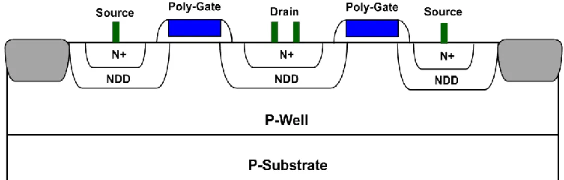
In this work, the power-rail ESD clamp circuit is proposed in a 162-nm 16-V double-diffused drain MOS (DDDMOS) process. The cross-sectional view of 16-V MOSFET with symmetric structure is shown in Fig. 2.1. By using a lightly doped drain drift region (NDD), the device can sustain high-voltage operation (16V). Fig. 2.2 shows the circuit scheme of power-rail ESD clamp circuit. According to the strong snapback phenomenon in the HV NMOS device during ESD stress, the traditional design using HV gate-grounded NMOS (GGNMOS) with a large device dimension was reported to suffer the non-uniform turn-on phenomenon [11]. Such a large device did not have a high ESD robustness after entering the snapback breakdown region. This is attributed to the current crowding effect among the multiple fingers and then inducing inhomogeneous triggering of the parasitic BJT to cause only several fingers of the device turned on under ESD stress. As a result, to efficiently improve the turn-on uniformity among those multiple fingers, the gate-driven design has been reported to increase ESD robustness of the device with large dimension [12]. As shown in Fig. 2.2, the ESD clamp circuit with gate-driven technique is designed to be turned on when the ESD voltage appears across the VCC and VSS power lines. On the contrary, the ESD clamp circuit is kept off when the IC is under the normal power-on condition. To meet these requirements, the time
constant in the VCC-to-VSS ESD clamp circuit is designed about 0.1–1μs to achieve the desired operations.
Fig. 2.1 The cross-sectional view of HV MOSFET in a 16-V DDDMOS process.
V
CCFig. 2.2 The circuit scheme of the gate-driven ESD clamp circuit.
The layout top view of the gate-driven ESD clamp circuit is shown in Fig. 2.3, where the W/L of HVMNESD is drawn as 1500 μm /1.2 μm. The device dimensions in
the ESD-transient detection circuit are chosen as R1 = 200 kΩ, C of HVMCAP = 1 pF,
W/L of HVMP1 = 100 μm /1.3 μm, and W/L of HVMN1 = 20 μm /1.2 μm. The resistor
of 200 kΩ is realized by a P+ poly resistance, and the capacitor of 1 pF is realized by a 16-V NMOS device. The RC time constant in the ESD-transient detection circuit is designed around ~0.2 μs to distinguish the ESD transient event from the power-on transition. Such a gate-driven ESD clamp circuit has been often used in the modern CMOS ICs.
2.2 Experimental Results
2.2.1 TLP-Measured Results and ESD Robustness
ESD robustness of the ESD clamp circuit is measured by TLP, HBM, and MM tests. A pulse width of 100 ns and a rise time of 10 ns are used in the TLP measurement setup. The failure criterion for It2 measurement is determined by leakage current which is greater than 1μA under voltage bias of 16 V. The voltage steps of TLP test are applied with 1 V. The TLP It2 of MESD is measured with 3
samples for double-check. The HBM and MM levels of the ESD clamp circuit are measured by the ESD tester, and the failure criterion is defined as the leakage current which is greater than 1 μA under voltage bias of 16 V. The voltage step of HBM test is 500 V, and the voltage step of MM test is 50 V. The HBM level and the MM level of MNESD are measured with 3 samples, respectively.
The experimental results are summarized in Table 2.1, including TLP, HBM, and MM tests. The ESD clamp circuit has ESD levels of over 8 kV in HBM and ~600 V in MM tests. The TLP-measured It2 is around 3.1 ~ 3.58 A. From the correlation equation of 3.58 A × 1.5 kΩ = 5.37 kV, the TLP-measured It2 with 1-V voltage step
has the estimated HBM level of 5.37 kV, which is lower than the ESD level (> 8kV) verified from the HBM ESD tester. The test results have an obvious deviation between TLP and HBM tests.
TABLE 2.1
TLP-measured results and ESD robustness of the gate-driven ESD clamp circuit
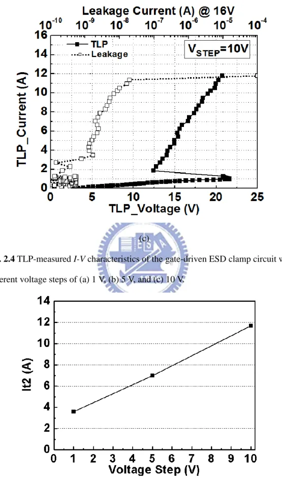
With a large deviation between the measured results of TLP test and HBM test, the unusual phenomenon should be studied. Therefore, different voltage steps of TLP tests in identical test circuit of the fabricated ESD clamp circuit are investigated. Fig. 2.4(a), 2.4(b), and 2.4(c) show the TLP-measured I-V characteristics of the gate-driven ESD clamp circuit with different voltage steps of 1 V, 5 V, and 10 V, respectively.Based on the TLP-measured results, the TLP-measured currents of the same ESD clamp circuit are ~1A before the HVMNESD enters the snapback region. After the snapback
occurs, the TLP-measured current is increased greatly when the applied TLP voltage is increased. However, the leakage current after snapback is also slightly increased (before the secondary breakdown point). When a 1-V voltage step is applied in the TLP test, the It2 is 3.58 A. When the voltage step is increased to 5 V, the It2 is increased to 7 A. Finally, with a 10-V voltage step, the It2 can be further increased up to 11.7 A. The dependency of TLP- measured It2 on the voltage step of TLP test is shown in Fig. 2.5. The TLP-measured It2 was increased when the voltage steps increasing.
(a)
(c)
Fig. 2.4 TLP-measured I-V characteristics of the gate-driven ESD clamp circuit with
different voltage steps of (a) 1 V, (b) 5 V, and (c) 10 V.
Fig. 2.5 Dependency of TLP-measured It2 on the voltage step of TLP test applied to
In the technical literature, a study was ever reported that the GGNMOS in a 43-V CMOS process had different TLP-measured It2 when different stress steps were used on two identical devices [13]. Fig. 2.6 shows the cross-sectional view of 43-V GGNMOS with symmetric structure. As shown in Fig. 2.7, the TLP-measured It2 of 43-V GGNMOS was increased with different pulse density. Low pulse density means large voltage step, and high pulse density means small voltage step. During high-current bipolar operation, the impact ionization hot-spot was located at the N+ diffusion (high injection mode) closely to the FOX bird’s beak. This behavior was also called kirk effect or base-push-out effect [14], [15]. As shown in Fig. 2.6, the red spots were used to represent charge trapping in the field oxide (FOX) at the bird’s beak under ESD stress. Therefore, this leakage increase reflected gradual device degradation when the parasitic BJT operated under high current conditions and was caused by a locally reduced junction breakdown voltage due to charge trapping in the field oxide. In addition, Fig. 2.8(a) showed the simplified TLP-measured I-V characteristics after repeated TLP measurement on the same test device. The trigger voltage was reduced with more and more repeated time. It was attributed to the charge trapped in field oxide which reduced the breakdown voltage locally, represented by the black spot in Fig. 2.8(b). As a result, the ESD stress current was localized at the black spot, preventing
uniform conduction through the whole finger of test device and lowering the trigger voltage.
G
S
D
Fig. 2.7 The TLP-measured It2 of GGNMOS in a high-voltage CMOS process with
different pulse density [13].
(a)
ESD stress current
(b)
Fig. 2.8 (a) The TLP-measured I-V characteristics with decreased trigger voltage in
repeated TLP measurement. (b) The top view of charge trapping in the field oxide locally and the distribution of ESD stress current in repeated TLP measurement [13].
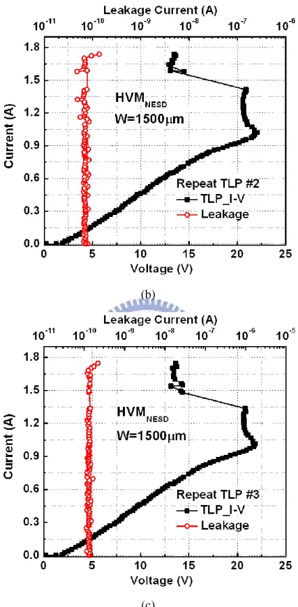
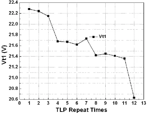
Based on the similar concept of the past study, the repeated TLP measurement is applied. The repeated TLP measurement setup is repeating TLP test until snapback without damaging circuit (TLP voltage from 0 V to 50 V in this case). The repeated TLP-measured results are shown in Fig. 2.9. The trigger voltage (Vt1) variation after repeated TLP measurement applied to the same ESD clamp circuit is recorded in Fig. 2.10. It is found that the trigger voltage (Vt1) is slightly decreased from 22 V to 20 V with more and more repeated time. According to the past study, the increased leakage current may reflect the charge trapping in gate oxide. Therefore, leakage current is measured in repeated TLP measurement. As shown in Fig. 2.11, the leakage is increasing with more and more repeated time. After TLP measurement with repeated time of 12, the test device is heated with 10 hours at 200 degrees Celsius to erase the trapped charge in gate oxide. However, the measured leakage current after annealing is increased. It means that the leakage current increasing is not caused by trapped charge. To further investigate this phenomenon, the failure analysis is applied in next part.
(b)
(c)
Fig. 2.9 TLP-measured I-V characteristics of the gate-driven ESD clamp circuit with
Fig. 2.10 Vt1 variation after repeated TLP measurement applied to the same ESD
clamp circuit.
Fig. 2.11 Leakage current variation after repeated TLP measurement applied to the
2.2.2 Failure Analysis
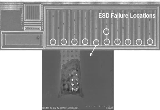
In order to investigate the physical failure mechanism of the identical ESD clamp circuits after TLP test of different voltage steps, the failure analysis is applied to seek the failure locations. In Fig. 2.12(a), with 1-V voltage step in TLP test, the failure locations are mainly located on few fingers of the HVMNESD device near to the ESD
detection circuit. In Figs. 2.12(b) and 2.12(c), with 5-V and 10-V voltage steps in TLP test, the failure locations are extended into more fingers of the HVMNESD device.
From the failure analysis pictures and TLP-measured results, non-uniform turn-on phenomenon among the multi-fingers of HVMNESD device become worse, especially
when the TLP test is applied with small voltage step.
To further investigate the non-uniform turn-on phenomenon, the failure analysis on the ESD clamp circuit after MM ESD test is shown in Fig. 2.13. After a 650-V MM ESD stress, the failure locations are located at all the fingers of HVMNESD
device.
(b)
(c)
Fig. 2.12 The OM and SEM pictures of the gate-driven ESD clamp circuit after TLP
Fig. 2.13 The SEM pictures of the gate-driven ESD clamp circuit after 650-V MM
stresses.
2.3 Discussion and Summary
2.3.1 Discussion
Among the TLP, HBM, and MM tests, the obvious difference is the zapping times. The more zapping times was applied, the HVMNESD device suffered the higher
cumulative energy. As a result, the cumulative energy during the TLP stresses of small voltage step is larger than that in HBM and MM tests. The experimental results indicated that the cumulative energy induce such a variation of the TLP-measured It2. However, the real mechanisms still cannot be found in this measurement results.
2.3.2 Summary
The power-rail ESD clamp circuit with gate-driven technique in a 16-V DDDMOS process has been fabricated to investigate its ESD robustness from the estimation of traditional correlation. Based on the failure analysis, the reason to cause
a deviation between TLP and HBM tests has been found. With different cumulative energy caused by different voltage steps in TLP test, different It2 values are obtained on the same ESD clamp circuit. As the voltage step is increased from 1V to 10V, the circuit exhibits higher TLP-measured It2 and the failure sites become more evenly distributed among the multiple fingers of MNESD, indicating that the device has been
uniformly turned on. This phenomenon can also be found in the failure analysis of MM test results.
Therefore, in order to get the TLP-measured It2 with well HBM correlation, the voltage-step dependency should be taken into consideration during TLP measurement, especially in the high-voltage CMOS processes. Moreover, the real physical mechanisms to cause the It2 variation also need to be further studied.
Chapter 3
Study of Safe Operating Area (SOA) and
Experiment Results
3.1 The Characterization of Safe Operating Area
High voltage and high current operations are common requirements for semiconductor devices in HV ICs. Safe operating area (SOA) in power semiconductors is one of the most important factors affecting device reliability [16]. The SOA region of HV MOSFET must be well characterized for using in circuit design to meet the specification of applications, which defines the operating limits without damaging the IC products.
The SOA specification is illustrated by the sketch in Fig. 3.1 [9]. It is an example showing different regions of SOA for a HV MOSFET. There are four regions in Fig. 3.1 which have respectively definition and meaning:
(1) Region A
It is limited by the turn-on resistance RDS,ON of the HV MOSFET.
(2) Region B
It is limited by the current carrying capability either from the HV MOSFET or the package.
(3) Region C
It is determined by the operating current and voltage across the HV MOSFET (power limited). In this thesis, it is the curve of electrical SOA (eSOA) which are measured with short pulse width by TLP system under fix TLP pulse width and different gate bias. When pulse width increases, region C moves downward due to the increasing
device self-heating and the electrothermal coupling. (4) Region D
It is defined by the maximum drain to source voltage rating, the BVDSS.
In Fig. 3.1, because boundaries are defined when turning the power transistor into on-state, it is referred to as the forward-biased SOA (FB-SOA).
SOA
Fig. 3.1 A Diagram showing SOA of a HV MOSFET[9].
FB-SOA is decided by the factors such as manufacture, material, package and device structure. In this thesis, the focus in FB-SOA is the curve of eSOA. The measurement setup of eSOA is shown in Fig. 3.2. Since snapback (triggering of the intrinsic BJT) usually causes irreversible damage to a HV MOSFET or circuit malfunctions, the eSOA boundary is defined by sweeping different gate biases and connecting the I-V points right before the device snapback. The mechanism of triggering of the intrinsic BJT is impact ionization in eSOA. The hot carriers get sufficient kinetic energy and transfer it into potential energy. The abundant electron-hole pairs make the junction breakdown and then turn on the parasitic BJT of HV MOSFET.
Fig. 3.2 The test setup for eSOA measurement by 100-ns TLP pulses [9].
For HV MOSFET designed to drive a considerable amount of current, ESD design rules were usually not applied to minimize their layout area. These HV MOSFET, as a result, were not capable of being self-protected against ESD stresses, and some additional ESD design techniques were needed to provide adequate capabilities to survive the general ESD specification of the 2-kV HBM ESD test for commercial products. Additional ESD clamp circuit in parallel to the HV MOSFET is one of the possible design solutions, but trigger competition between the ESD clamp circuit and the HV MOSFET can usually lead to an upset result on the ESD protection level. As a result, self-protected HV MOSFETs are preferable to HV ICs. It is important to have a deeper investigation on the structure of HV MOSFET to get win-win solution for SOA and ESD robustness.
3.2 The Test Devices in a 60-V BCD Process
In this section, the characterization of eSOA and the modified structures for ESD improvement of HV MOSFETs are presented with the experimental data. The standard device structure of nLDMOS in a 0.25-μm 60-V BCD process is shown in Fig. 3.3. The operating voltage region is VDS = 0 ~ 60V and VGS = 0 ~ 5V. The HV
device is surrounded by N-buried layer (NBL) to separate HVPW and P-substrate. The deep P well (DPW) is used for RESURF technology to enhance the breakdown voltage (BVDSS) without paying layout area for high on-resistance (RDS,ON).
(a)
(b)
Fig. 3.3 The (a) cross-sectional view and (b) top view of Standard nLDMOS in a
60-V BCD process.
In this work, the DPW structure of nLDMOS is modified to investigate the influence of DPW structure on ESD performance. The test devices include standard
device nLDMOS_S, modified device nLDMOS_A, and modified device nLDMOS_B. As shown in Fig. 3.4, the DPW structure under drain side is erased in nLDMOS_A.
(a)
(b)
Fig. 3.4 The (a) cross-sectional view and (b) top view of modified nLDMOS_A in a
60-V BCD process.
The other test device structure of nLDMOS_B is shown in Fig. 3.5. The DPW structure is slotted under the region of drain OD. Based on the past study [17], the slotted DPW structure can make a vertical BJT path where ESD current can flow into
NBL region. It is expected to enhance the ESD robustness. All the test devices are chosen as W/L = 320 μm/ 1μm. The region of drain OD, represented by distance X, is changed with 0.14μm, 5μm, and 10μm, respectively, in all the test devices. The other layout parameters are the same as the standard device structure, which are not changed in this work.
(a)
(b)
Fig. 3.5 The (a) cross-sectional view and (b) top view of modified nLDMOS_B in a
3.3 Experimental Results
3.3.1 Measurement Results of Electrical SOA
In this work, electrical SOA (eSOA) is measured by 100-ns TLP pulses when giving a DC voltage for gate bias. The gate bias is varied from 0 V to 5 V. The breakdown voltage (BVDSS) of the test devices are summarized in Table 3.1. Fig. 3.6
shows the measured eSOA of nLDMOS_S with W = 320μm and X = 0.14μm, 5μm, and 10 μm, respectively. The tests Devices with IDS from low to high are measured
under gate biases of 0, 1, 3, and 5 V. The region of eSOA is slightly extended with a wide drain region when using large distance X. The breakdown voltage for nLDMOS_S is about 77 V. Next, the eSOA of nLDMOS_A and nLDMOS_B are shown in Fig. 3.7 and Fig. 3.8, respectively. Their eSOA can be obviously extended with large distance X. The breakdown voltage for nLDMOS_A and nLDMOS_B is about 53 V and 74 V, respectively. According to the comparison of different eSOA with nLDMOS_S, nLDMOS_A, and nLDMOS_B in Fig. 3.9, the eSOA of nLDMOS_A is the greatest; in contrast, the eSOA of nLDMOS_S is the worst. The nLDMOS_B with slotted DPW structure can have a better eSOA than nLDMOS_S. Although the breakdown voltage of nLDMOS_A is lower than 60 V, its eSOA is the widest region.
TABLE 3.1
(a)
(c)
(d)
Fig. 3.6 The I-V characteristics of nLDMOS_S with different distance X of (a)
0.14μm, (b) 5μm, and (c) 10 μm, respectively, measured by 100-ns TLP system. (d) The eSOA of nLDMOS_S with different distance X.
(a)
(c)
(d)
Fig. 3.7 The I-V characteristics of nLDMOS_A with different distance X of (a)
0.14μm, (b) 5μm, and (c) 10 μm, respectively, measured by 100-ns TLP system. (d) The eSOA of nLDMOS_A with different distance X.
(a)
(c)
(d)
Fig. 3.8 The I-V characteristics of nLDMOS_B with different distance X of (a)
0.14μm, (b) 5μm, and (c) 10 μm, respectively, measured by 100-ns TLP system. (d) The eSOA of nLDMOS_B with different distance X.
(a)
(c)
Fig. 3.9 The comparison of measured eSOA with nLDMOS_S, nLDMOS_A, and
nLDMOS_B.
3.3.2TLP-Measured Results and ESD Robustness
The following is the ESD experimental results of different test devices. Fig. 3.10 ~ 3.12 show the TLP-measured results under the same condition of VGS = 0 V. The
solid line presents the TLP-measured I-V curves while the dotted line is the leakage current which is measured after every TLP stress pulse. The data of trigger voltage (Vt1), trigger current (It1), holding voltage (Vhold), and secondary breakdown current
(It2) are extracted from TLP-measured I-V curves, as shown in Table 3.2. According to the TLP-measured I-V characteristics, no snapback region is observed in these test devices. The tests devices immediately failed as the snapback happened. As a result, the data of trigger voltage and trigger current are not available. The test device nLDMOS_S has ESD levels of 0.3 kV ~ 0.5 kV in HBM tests, below 50 V ~ 50V in MM tests, and It2 of 0.085 A ~ 0.15 A in TLP measurement with different distance X.
Next, the test device nLDMOS_A has ESD levels of 0.5 kV ~ 0.8 kV in HBM tests, 50 V ~ 100V in MM tests, and It2 of 0.16 A ~ 0.27 A in TLP measurement with different distance X. Moreover, the test device nLDMOS_B has ESD levels of 0.5 kV ~ 0.7 kV in HBM tests, 50 V ~ 100V in MM tests, and It2 of 0.14 A ~ 0.25 A in TLP measurement with different distance X. The ESD performance of test devices can be improved with a large distance X of 10 μm. Compared with the measured results in Table 3.2, the ESD performance of nLDMOS_A is the greatest; on the contrary, nLDMOS_B is the worst.
Fig. 3.10 TLP-measured I-V characteristics of nLDMOS_S with different distance X
Fig. 3.11 TLP-measured I-V characteristics of nLDMOS_A with different distance X
of 0.14μm, 5μm, and 10 μm.
Fig. 3.12 TLP-measured I-V characteristics of nLDMOS_B with different distance X μm, 5μm, and 10 μm.
TABLE 3.2
The TLP-measured results and ESD robustness with different test devices
Device (W=320μm)
( VGS=0V )
Curve
Tracer TLP ESD tester
BVDSS (V) Vt1 (V) Vhold (V) It2 (A) Positive HBM (kV) MM (V) nLDMOS_S (X=0.14μm) 77 -- -- 0.085 0.3 < 50 nLDMOS_S (X=5μm) 78 -- -- 0.12 0.4 50 nLDMOS_S (X=10μm) 78 -- -- 0.15 0.5 50 nLDMOS_A (X=0.14μm) 53 -- -- 0.16 0.5 50 nLDMOS_A (X=5μm) 56 -- -- 0.21 0.6 100 nLDMOS_A (X=10μm) 56 -- -- 0.27 0.8 100 nLDMOS_B (X=0.14μm) 74 -- -- 0.14 0.5 50 nLDMOS_B (X=5μm) 75 -- -- 0.21 0.6 100 nLDMOS_B ( X=10μm) 75 -- -- 0.25 0.7 100
3.4 Discussion and Summary
3.4.1 Discussion
As shown in Fig. 3.13, the similar report showed that a 50-V RESURF nLDMOS had increased TLP-measured It2 with a deep drain profile engineering [17]. In the deep drain case, a deep n+ sinker was implanted below the drain junction and overlaps it so that the connection from NBL to drain was accomplished internally.
The effective drift length of the deep drain device was the same as the shallow drain case. The breakdown voltage for the deep drain device showed a slightly degraded tradeoff compared with the shallow drain case. In the deep drain structure, the parasitic BJT current could flow vertically into the NBL region. The vertical bipolar current was spread almost along the entire length of the device cross section, resulting in a significant reduction of the power density. The sharp localized temperature increase near the drain junction was thus avoided. Hence, the TLP-measured It2 of a deep drain device that was higher than in the shallow drain device could be obtained.
Shallow Drain Deep Drain
(a)
(b)
Fig. 3.13 (a) The cross-sectional view and (b) TLP-measured I-V characteristics of
In this work, the parasitic BJT of 60-V nLDMOS still cannot be turned on even if the DPW structure is totally erased in the test results of nLDMOS_A. The most likely reason for the difficulty of turn-on issue is the extremely low base resistance in parasitic BJT path. The base resistance is reduced dramatically with the HVPB structure. As a result, the parasitic BJT path cannot be turned on efficiently after breakdown happens.
3.4.2 Summary
The test devices for study of self-protected HV MOSFET have been investigated with the modified DPW structure in a 60-V BCD process. According to the measurement results, nLDMOS_B with slotted DPW structure can maintain high breakdown voltage and get win-win solution for wide SOA and better ESD robustness at the same time. However, the ESD robustness still cannot be improved effectively in this work due to the lack of parasitic BJT path. To protect the HV devices against ESD stresses, the extra ESD clamp circuit should be additionally added outside the internal circuits.
Chapter 4
Study
of
ESD
Protection
Circuits
and
Experiment Results
4.1 The Proposed ESD Design in a 60-V BCD Process
As mentioned in Chapter 3, Such HV transistors did not have enough self-protected ability against ESD stresses. Therefore, an additional ESD protection design is needed to protect such HV transistors of output drivers in HV applications. To protect the HV output drivers against ESD stresses, the additional ESD protection circuit is placed in parallel with the output drivers from the output pad (O/P) to the VSS. If the additional ESD protection circuit was not turned on quickly enough, the output driver would be damaged during an ESD stress event. As a result, it is important to develop an efficient ESD protection circuit that can effectively protect the HV output drivers for various applications [18], [19].
In this work, the ESD protection circuits are proposed in a 0.25-μm 60-V BCD process, including gate-driven nLDMOS, gate-driven nLDMOS with embedded SCR, gate-driven nLDMOS with self-substrate-triggered technique, and the gate-driven nLDMOS with self-substrate-triggered technique and embedded SCR. The proposed ESD protection designs with the gate-driven ESD detection circuit will be introduced in the following.
4.1.1 The Gate-Driven nLDMOS
Fig. 4.1 shows the circuit scheme and cross-sectional view of gate-driven nLDMOS. The main ESD clamp device MESD is implemented by nLDMOS with
slotted DPW structure. As discussed in Chapter 3, the nLDMOS with slotted deep P-well (DPW) structure can have good ESD robustness and maintain high breakdown voltage at the same time. The channel width of nLDMOS is 800μm, and the distance X is 5μm. The other layout parameters are the same as the standard device structure.
The ESD detection circuit is composed of a HV diode and a 10-kΩ resistor. The reverse-biased HV diode is used to sustain the high-voltage applications during the normal circuit operating condition. The trigger voltage can be tunable individually with the breakdown voltage of HV diode. The ESD protection circuit with gate-driven technique is designed to be turned on when the ESD voltage appears across the VCC and VSS power lines. On the contrary, the ESD protection circuit is kept off when the IC is under the normal power-on condition. To meet these requirements, the breakdown voltage of HV diode should be designed as 1.2 times of VCC to avoid mistriggering. (In this work, it is convenient to fabricate the ESD detection circuit with standard HV diode whose breakdown voltage is 57V. However, the breakdown voltage should be designed for required specification.)
When a positive ESD stress is applied to the O/P with VSS grounded, the HV diode will enter the breakdown mode to conduct some of ESD current across the 10-kΩ resistor to generate a bias voltage to the gate of MESD. Thus, the gate voltage of
MESD can be quickly pulled up to turn itself on during ESD stress. When the gate bias
of MESD is increased, the channel current is generated to induce the turn-on path of the
(a)
(b)
Fig. 4.1 (a) The circuit scheme of gate-driven nLDMOS and (b) the cross-sectional
view of nLDMOS.
4.1.2 The Gate-Driven nLDMOS with Embedded SCR
Fig. 4.2 shows the gate-driven nLDMOS_SCR in a 60-V BCD process. The main ESD clamp device MESD is named as nLDMOS_SCR with slotted DPW structure and
embedded SCR structure. The channel width of nLDMOS_SCR is 800 μm, and the distance X is 5μm. The drain side is added with P+ region near N+ region to construct SCR path. The other layout parameters are the same as the standard device structure.
Based on the previous reports [20]-[24], the inserted SCR structure can improve ESD robustness. The device is expected to combine the characteristic of both nLDMOS and SCR.
(a)
(b)
Fig. 4.2 (a) The circuit scheme of gate-driven nLDMOS_SCR and (b) the
cross-sectional view of nLDMOS_SCR.
4.1.3 The Gate-Driven nLDMOS with Self-Substrate-Triggered Technique
Fig. 4.3 shows the gate-driven SST_nLDMOS with self-substrate-triggered technique in a 60-V BCD process. The main ESD clamp device MESD is named as
SST_nLDMOS with slotted DPW structure and modified device structure. The channel width of SST_nLDMOS is 800 μm, the distance X is 5 μm, and the distance Y is 1 μm. The source side is modified with a trigger node that channel current can flow into substrate as a substrate current. It is expected that the substrate current can enhance parasitic NPN BJT of MESD which will improve the ESD robustness.
VCC
VSS
10kΩ SST_nLDMOS HV Diode MESD N P N P+ (a) (b)Fig. 4.3 (a) The circuit scheme of gate-driven SST_nLDMOS with
4.1.4 The Gate-Driven nLDMOS with Self-Substrate-Triggered Technique and Embedded SCR
Fig. 4.4 shows the gate-driven nLDMOS_SCR with self-substrate-triggered technique in a 60-V BCD process. The main ESD clamp device MESD is named as
SST_nLDMOS_SCR with slotted DPW structure, modified device structure, and embedded SCR. The channel width of SST_nLDMOS_SCR is 800 μm, the distance X is 5 μm, and the distance Y is 1 μm. It is expected that the substrate current can enhance SCR path of MESD which will improve the ESD robustness effectively.
P+ HVNW N+ HVPW P+ HV Diode 10kΩ
VCC
VSS
SST_nLDMOS_SCR MESD (a)Fig. 4.4 (a) The circuit scheme of gate-driven SST_nLDMOS_SCR and (b) the
4.2 Experimental Results
4.2.1 TLP-measured Results and ESD Robustness
As illustrated in Fig. 4.5, the main ESD protection devices and the ESD detection circuit are drawn individually on the same layout area. If the gate-driven ESD protection circuit was damaged by ESD stress, the leakage current could be measured individually to check the damaged cell.
Fig. 4.5 The measurement setup to verify ESD performance.
Fig. 4.6 - 4.9 show the TLP-measured results of different ESD protection circuits with and without ESD detection circuit, respectively. The solid line presents the TLP-measured I-V curves while the dotted line is the leakage current which is measured after every TLP stress pulse. The data of trigger voltage (Vt1), trigger current (It1), holding voltage (Vhold), and secondary breakdown current (It2) are
extracted from TLP-measured I-V curves, as shown in Table 4.1. As mentioned in Chapter 2, the voltage-step dependency should be taken into consideration in HV processes. Therefore, the different voltage steps of 1V and 5V are used in these 60-V
test devices. The gate-grounded nLDMOS has ESD levels of 1 kV in HBM tests, 100 V in MM tests, and It2 of 0.46 A ~ 0.53 A in TLP measurement with different voltage steps. With the ESD detection circuit, the gate-driven nLDMOS has ESD levels of 2.5 kV in HBM tests, 150 V in MM tests, and It2 of 2.3 A ~ 3.4 A in TLP measurement with different voltage step. Next, the gate-grounded nLDMOS_SCR has ESD levels of 1 kV in HBM tests, 100 V in MM tests, and It2 of 0.49 A ~ 0.53 A in TLP measurement with different voltage steps. With the ESD detection circuit, the gate-driven nLDMOS_SCR has ESD levels of 2.5 kV in HBM tests, 150 V in MM tests, and It2 of 2.04 A ~ 2.44 A in TLP measurement with different voltage steps. Moreover, the gate-grounded SST_nLDMOS has ESD levels of 1 kV in HBM tests, 100 V in MM tests, and It2 of 0.38 A ~ 0.39 A in TLP measurement with different voltage steps. With the ESD detection circuit, the gate-driven SST_nLDMOS has ESD levels of 3 kV in HBM tests, 200 V in MM tests, and It2 of 1.85 A ~ 5.78 A in TLP measurement with different voltage steps. Finally, the gate-grounded SST_nLDMOS_SCR has ESD levels of 1 kV in HBM tests, 100 V in MM tests, and It2 of 0.39 A ~ 0.4 A in TLP measurement with different voltage steps. With the ESD detection circuit, the gate-driven SST_nLDMOS_SCR has ESD levels of 3 kV in HBM tests, 200 V in MM tests, and It2 of 3.16 A ~ 6.74 A in TLP measurement with different voltage steps.
According to the TLP-measured I-V characteristics, there is no snapback region observed in these gate-grounded test devices. Such test devices immediately failed as the snapback happened. As a result, the data of trigger voltage and trigger current are not available in these gate-grounded test devices. On the contrary, the parasitic BJT of test devices can be turned on with ESD detection circuit. The It2 of test devices are increased greatly with large voltage step after test devices enter snapback region.
(a)
(b)
Fig. 4.6 The TLP-measured I-V characteristics of (a) gate-grounded nLDMOS (b)
(a)
(b)
Fig. 4.7 The TLP-measured I-V characteristics of (a) gate-grounded nLDMOS_SCR
(a)
(b)
Fig. 4.8 The TLP-measured I-V characteristics of (a) gate-grounded SST_nLDMOS
(a)
(b)
Fig. 4.9 The TLP-measured I-V characteristics of (a) gate-grounded
TABLE 4.1
TLP-measured results and ESD robustness with different ESD protection circuits
Circuit BV
(V)
TLP (Step=1V) TLP (Step=5V) ESD tester
Vt1 (V) Vhold (V) It2 (A) Vt1 (V) Vhold (V) It2 (A) Positive HBM (kV) MM (V) Stand-alone nLDMOS (VG=0V) 75 -- -- 0.53 -- -- 0.46 1 100 Gate-driven nLDMOS 57 58.29 18.06 2.3 58.56 15.99 3.4 2.5 150 Stand-alone nLDMOS_SCR (VG=0V) 74 -- -- 0.53 -- -- 0.49 1 100 Gate-driven nLDMOS_SCR 57 57.27 18.6 2.04 52.83 16.49 2.44 2.5 150 Stand-alone SST_nLDMOS (VG=0V) 74 -- -- 0.39 -- -- 0.38 1 100 Gate-driven SST_nLDMOS 57 65.55 20.66 1.85 65.45 19.77 5.78 3 200 Stand-alone SST_nLDMOS_SCR (VG=0V) 74 -- -- 0.4 -- -- 0.39 1 100 Gate-driven SST_nLDMOS_SCR 57 69.64 19.82 3.16 65.88 18.43 6.74 3 200
According to the measurement results, the ESD performance of test devices with embedded SCR cannot be improved greatly and their holding voltage are almost the same as that without embedded SCR. Furthermore, compared with the measured results of gate-driven nLDMOS and nLDMOS_SCR, the ESD performance of gate-driven SST_nLDMOS and SST_nLDMOS_SCR can have better ESD robustness
due to self-substrate-triggered technique. Besides, the ESD levels in HBM and MM tests are lower than equivalent level of TLP-measured It2, especially in test results of gate-driven SST_nLDMOS and SST_nLDMOS_SCR when using large voltage step of 5 V. This may be attributed to the gate-oxide overstress from ESD detection circuit [25]. As illustrated in Fig. 4.10, the gate oxide of gate-driven nLDMOS has been damaged to induce leakage current from gate to source (IGS) after 3-kV HBM stress.
(a)
(b)
Fig. 4.10 (a) The scheme of damaged site in gate-driven nLDMOS and (b) the
4.2.2 The ESD Robustness with Optimized Measurement Setup
Due to the overstress from ESD detection circuit in HBM and MM tests, the gate oxide of main ESD protection devices would be damaged easily. Such a device suffers gate-oxide overstress before reaching its intrinsic ESD robustness. The HBM and MM levels are smaller than the equivalent level of TLP-measured It2. As a result, it suggests that the protection elements must be added to protect the gate oxide, including 1-kΩ resistor and clamping device (9-V Zener diode), as illustrated in Fig. 4.11. The breakdown voltage of gate oxide is about 13V. Therefore, a 9-V Zener diode below breakdown voltage can be used to clamp the overstress voltage. With the optimized measurement setup, the improved ESD levels are shown in Table 4.2.
TABLE 4.2
The ESD robustness with and without optimized measurement setup
Circuit ESD tester (Without optimized measurement setup) ESD tester (With optimized measurement setup) HBM (kV) MM (V) HBM (kV) MM (V) Gate-driven nLDMOS 2.5 150 3.5 200 Gate-driven nLDMOS_SCR 2.5 150 3.5 200 Gate-driven SST_nLDMOS 3 200 4 250 Gate-driven SST_nLDMOS_SCR 3 200 4 250
4.3 Discussion and Summary
4.3.1 Discussion
The gate oxide can be damaged easily by the overstress from ESD detection circuit in HBM and MM tests. Therefore, the HBM and MM levels are smaller than the equivalent level of TLP-measured It2. It suggests that the protection elements must be added to protect the gate oxide, including RESD and clamping device, as
shown in Fig. 4.12.
According to the experimental results, the new structure of nLDMOS with self-substrate-triggered technique is proposed and verified. Compared with
![Fig. 1.1 Typical design of on-chip ESD protection circuits in HV ICs [6].](https://thumb-ap.123doks.com/thumbv2/9libinfo/8761049.208181/15.892.201.692.328.698/fig-typical-design-chip-esd-protection-circuits-ics.webp)
![Fig. 1.2 ESD protection design window of HV ESD protection device [7].](https://thumb-ap.123doks.com/thumbv2/9libinfo/8761049.208181/16.892.159.725.149.702/fig-esd-protection-design-window-esd-protection-device.webp)
![Fig. 2.6 The cross-sectional view of HV GGNMOS with symmetric structure [13].](https://thumb-ap.123doks.com/thumbv2/9libinfo/8761049.208181/28.892.217.686.939.1080/fig-cross-sectional-view-hv-ggnmos-symmetric-structure.webp)
![Fig. 3.1 A Diagram showing SOA of a HV MOSFET [9].](https://thumb-ap.123doks.com/thumbv2/9libinfo/8761049.208181/38.892.242.656.319.720/fig-diagram-showing-soa-hv-mosfet.webp)
![Fig. 3.2 The test setup for eSOA measurement by 100-ns TLP pulses [9].](https://thumb-ap.123doks.com/thumbv2/9libinfo/8761049.208181/39.892.315.586.112.369/fig-test-setup-esoa-measurement-ns-tlp-pulses.webp)
