行政院國家科學委員會專題研究計畫 期中進度報告
在矽基板整合 40 奈米三五族與鍺量子井場效電晶體作為低
功率與高速無線之應用(2/3)
期中進度報告(精簡版)
計 畫 類 別 : 整合型 計 畫 編 號 : NSC 99-2120-M-009-005- 執 行 期 間 : 99 年 08 月 01 日至 100 年 07 月 31 日 執 行 單 位 : 國立交通大學材料科學與工程學系(所) 計 畫 主 持 人 : 張翼 共 同 主 持 人 : 劉致為、孟慶宗、呂志鵬、許恆通 報 告 附 件 : 國外研究心得報告 處 理 方 式 : 本計畫涉及專利或其他智慧財產權,2 年後可公開查詢中 華 民 國 100 年 09 月 07 日
行政院國家科學委員會補助專題研究計畫
□ 成 果 報 告
▓期中進度報告
(計畫名稱)
在矽基板整合 40 奈米三五族與鍺量子井場效電晶體作為低功率與高速無線之
應用
計畫類別:□ 個別型計畫 ▓ 整合型計畫
計畫編號:NSC 99-2120-M-009-005-
執行期間:2010 年 08 月 01 日至 2011 年 07 月 31 日
計畫主持人:張 翼
共同主持人:張俊彥 國家講座教授、劉致為 教授、孟慶宗 教授、呂志
鵬 副教授、許恆通 副教授
計畫參與人員: 林岳欽、郭建億、張家源、徐慶議、王景德、張家達、
唐士軒、蘇詠萱、金海光、邱昱盛、蔡思屛、陳哲霖、游嘉惠、涂勝翰
與陳玉芳等。
成果報告類型(依經費核定清單規定繳交):▓精簡報告 □完整報告
本成果報告包括以下應繳交之附件:
□赴國外出差或研習心得報告一份
□赴大陸地區出差或研習心得報告一份
▓出席國際學術會議心得報告及發表之論文各二份
□國際合作研究計畫國外研究報告書一份
處理方式:除產學合作研究計畫、提升產業技術及人才培育研究計畫、
列管計畫及下列情形者外,得立即公開查詢
▓涉及專利或其他智慧財產權,□一年▓二年後可公開查詢
執行單位:
中 華 民 國 100 年 9 月 日
一、中文摘要 關鍵字:量子井場效電晶體、砷化銦、超低功率、數位邏輯、原子層氣相沉積、表面處理
目前矽半導體工業技術已經面臨其物理極限,新穎半導體材料迫切需求來替代原來矽 通道材料,如鍺、砷化銻、砷化銦鎵或砷化銦來當作後矽奈米世代高速低功耗邏輯應用, 近年研究顯示與證實三五族異質場效電晶體之優勢電性由於其高電子遷移率與成熟製程技 術,三五材料的傑出低電場傳輸特性亦使得元件可以在低操作電壓下運作,因此本研究在 元件部分報告 40 奈米砷化銦電晶體在低電壓下優異的數位邏輯電性。 在三五族半導體與高介電常數材料整合部分,原子層氣相沉積氧化鋁/砷化銦鎵金氧半 電容之反轉行為在不同退火條件與表面處理條件下仔細探討其物性與電性,在結合濕式硫 化與乾式 TMA 下可以觀察出電容強反轉行為。砷化銦電容在結合濕式硫化、鹽酸表面處 理與乾式 TMA 等預處理下,其電性與物理特性亦透過 XPS 與電性模擬仔細探討,以做為 未來砷化銦 CMOS 之應用或是 MOS QWFET 等元件應用,實驗結果顯示累積電容行為不會 受到介面態缺陷的影響且與表面處理沒有太大影響,研究同時顯示鹽酸/TMA 預處理可以 有效降低類施體缺陷而產生強反轉與硫化/TMA 相較。
二、英文摘要
Keywords: Quantum-Well FET, InAs, ultra-low power, digital logic, atomic layer deposition (ALD), surface treatment
Current Si-CMOS technology has come to a limit that novel semiconductors as alternative channel materials (Ge, InSb, InxGa1-xAs, InAs) are urgently needed for high-speed and
low-power logic devices for post CMOS era. Recent research shows III-V heterostructure field-effect transistors demonstrate aggressive merits due to its high electron mobility and rather mature process technology. The outstanding low field electron transport characteristics of III-V materials make ultrahigh-speed switching at very low supply voltage possible. Therefore, we present the latest advancement of 40 nm InAs/InxGa1-xAs composite channel Quantum-Well FET
that have achieved excellent digital logic characteristics at very low supply voltage.
For the high-κ/III-V integration, the inversion behaviors of atomic-layer-deposition Al2O3/n-In0.53Ga0.47As metal-oxide semiconductor capacitors are also studied by various surface
treatments and post deposition annealing using different gases. By using the combination of wet sulfide and dry trimethyl aluminum (TMA) surface treatment along with pure hydrogen annealing,
HCl-plus-TMA treatment has a stronger effect on the reduction of donorlike traps than the sulfide-plus-TMA treatment.
三、報告內容 1. Introduction
For device scaling in Si technology, the physical gate length of Si transistors used in the current 65 nm generation node is about 30 nm and the size of the transistor will reach 10 nm in 2012. Recently, the International Technology Roadmap of Semiconductors also forecasted integration of planar III-V compound semiconductor FETs with Si technology is one of the promising solutions for the future post-Si CMOS technology to extend Moore’s law well into the next decade [1]. These main reasons are due to their outstanding electron transport properties, their relative maturity, and demonstrated reliability when compared with other candidates, such as carbon nanotube transistors and semiconductor nanowires [2]. Generally, the extremely high transconductance and excellent RF performance have been demonstrated recently by InAlAs/InxGa1-xAs MHEMTs on GaAs substrate or InP substrate with ultra short gate length
[3,4].
Low DC power consumption is always a highly desired property for practical system applications. However, maintaining device performance with low drain bias can only be achieved through optimized device technology which also plays a critical role for high-speed low-power digital applications. Having the properties of electron mobility as high as 20,000 cm2/Vs at room temperature, higher electron peak velocity, low electron effective mass and a reasonable energy bandgap (0.36 eV), InAs materials have attracted numerous attentions as transistor-channel of Quantum Well FETs (QWFETs) for future high-speed and low-power digital applications [5].
In the meantime, compared with numerous studies of high-k/GaAs and InGaAs structures, the study of the high-k/InAs structure is still relatively unexplored. Aside from the application in the inversion-mode MOS field-effect transistor, the application of InAs as a channel for MOS QWFETs is also very promising [6,7]. As a result, we also study the electrical characteristics of atomic layer deposition (ALD) Al2O3/n-InAs with various surface treatments, including sulfide
and HCl treatments in conjunction with an in situ trimethyl aluminum (TMA) pretreatment. Experimental results and C–V simulations are combined to investigate the electrical properties of Al2O3/InAs MOSCAP structures. Effects of surface treatments on the C–V behavior in
accumulation, depletion, and inversion regimes are discussed [8].
2. Result and Discussion
The aim of this project is to develop 40-nm III-V QWFETs and Ge QWFETs on the Si substrate for future post CMOS logic and high speed RF applications. For 40-nm InAs QWFETs development, in order to avoid the short channel effect (SCE), the QWFET was fabricated by reducing gate to channel distance. The QWFET was also careful evaluated in terms of impact ionization at different drain bias voltage. Fig. 1 shows the I-V characteristics and transconductance improvement with vertical scaling of the device using two-step recess and Pt-buried gate technique.
The 40 nm device exhibits improved performance such as better current saturation, lower output conductance, and smaller threshold voltage shift after scaling. The RF and logic performances of 40 nm device are shown in Fig. 2 and Fig. 3. The gate delay time was evaluated to be 0.62 psec at 0.5 volt drain bias.
Fig. 1 (a) DC characteristics of 40 nm device without vertical scaling (Pt gate on InP layer)
Fig. 1 (b) DC characteristics of 40 nm device with vertical scaling (Pt-buried gate on InAlAs layer)
Fig. 1 (c) The transconductance of devices with 80 nm and 40 nm
Fig. 1 (d) The 40 nm HEMTs with different gate structure. They are conventional gate, two-step gate and the two-step gate with Pt-buried gate. Device with thinner schottky barrier improves the transconductance and also the threshold voltage move positive.
Fig. 2 Frequency dependence of the current-gain and the Mason’s unilateral gain of 40-nm InAs
HEMTs. A higher fT of 423 GHz
and fmax of 184 GHz were obtained
for device with thinner insulator as compared to the conventional device with an fT of 395 GHz and an
fmax of 111 GHz.
Fig. 3 the thinner barrier device shows less DIBL due to the improvement of SCE.
We also report the first result of a strained In0.52Ga0.48As channel high electron mobility
transistor featuring highly doped In0.4Ga0.6As source/drain (S/D) regions. The schematic of
conventional device structure and the proposal strained device structure are shown in Fig.4. A lattice mismatch of 0.9 % between the channel material (In0.52Ga0.48As) and S/D material
(In0.4Ga0.6As) has resulted in a lateral strain in the In0.52Ga0.48As channel region, where the series
Fig. 4 Schematics of (a) conventional In0.52Ga0.48As
channel HEMT and (b) proposed In0.52Ga0.48As channel
HEMT with heavily doped In0.4Ga0.6As S/D region.
Fig. 5 Comparison between conventional and proposed device. (a) Transconductance versus gate voltage. (b) Current gain versus frequency.
Fig. 6 Comparison of average electron velocity between conventional and proposed device.
Fig. 7 Comparison of electron mobility between
conventional and proposed device.
Strong inversion was observed for the MOS capacitor with interface trap density less than 5×10¹¹ ev-1cm-2 by the simple surface treatment method. Fig. 8 shows the multifrequency C-V responses of ALD Al2O3/n-In0.53Ga0.47As MOS capacitor and the inset in this figure shows the
corresponding G-V curves. The XPS spectra of the capacitors with different surface treatment conditions are shown in Fig. 9.
The material and electrical characteristics of ALD Al2O3/InxGa1-xAs structure with In
content of 0.53, 0.7 and 1.0 were investigated, the frequency dispersion、hysteresis、Dit
distribution、leakage current are quite small provided proper surface treatment methods were used.
Fig. 10 and Fig. 11 present C-V characteristics and interface trap density of the MOS capacitors. The studied Dit, frequency dispersion, C-V hysteresis, are among the smallest reported in
literatures.
Ex situ sulfide and HCl wet chemical treatments in conjunction with in situ trimethyl
aluminum (TMA) pretreatment were performed before the deposition of Al2O3 on n-InAs
oxides after different treatments. Fig. 12 shows the C–V characterization of Al2O3 /n-InAs
structures. The frequency dispersion in the accumulation regime is small (<0.75 %/dec) and does not seem to be significantly affected by the different surface treatments. The interface trap density profiles extracted from the simulation is shown in Fig. 13. It shows donorlike interface states inside the InAs band gap and in the lower part of the conduction band. Low interface trap density in the range of 1012 eV-1cm-2 was achieved by this simple surface treatment method.
Fig. 8 Multifrequency C-V responses in sulfide+TMA
treated Al2O3 / n-In0.53Ga0.47As MOSCAPs, with PDA
in H2 gas. The inset in Fig. 8 shows the
conductance-voltage (G-V) characteristics.
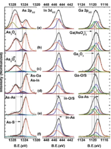
Fig. 9 The As 2p3/2, In 3d5/2, Ga 2p3/2 XPS spectra of (a)
native oxide-covered InGaAs surface; (b) TMA treated sample, with ALD Al2O3, as deposited; (c)
sulfide+TMA treated sample, with ALD Al2O3, as
deposited; (d) TMA treated sample, with ALD Al2O3,
after PDA in N2; (e) sulfide+TMA treated sample, with
ALD Al2O3, after PDA in N2; (f) sulfide+TMA treated
sample, with ALD Al2O3, after PDA in H2.
Fig. 10. (a) C-V responses of samples at 1 MHz, the C-V behaviors change from high frequency like for In0.53Ga0.47As to low frequency like for InAs; The multi-frequency C-V response and bidirectional C-V response at
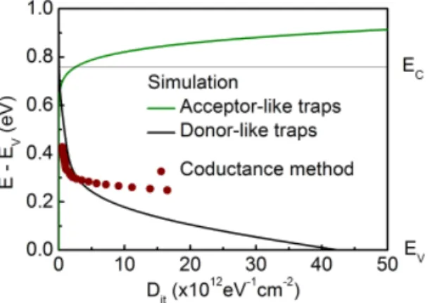
Fig. 11. The distribution of Dit at Al2O3/In0.53Ga0.47As structure achieved by simulation and conductance method.
Fig. 12 Multifrequency C-V responses and QSCV curve (a) control sample (b) HCl/TMA treated sample (c) sulfide/TMA treated sample (d) QSCV curve of all three samples for comparison
Fig. 13 (a) (Symbols) Experimental data and (solid lines) simulated C–V curves of ALD Al2O3/n-InAs
MOSCAP samples with various surface treatments. Interface state density profiles of all three samples, extracted fromsimulation (b) the control sample, (c) the HCl-plus-TMA-treated sample, and (d) the sulfide-plus-TMA-treated sample.
Reference:
1. J. A. del Alamo, and D. H. Kim, “Beyond CMOS: Logic Suitability of InGaAs HEMTs,” in 19th International Conference on Indium Phosphide and Related Materials, Matsue, Japan, 14 - 18 May 2007.
2. R. Chau, “III–V on silicon for future high speed and ultra-low power digital applications: Challenges and opportunities,” in Proc. CS-MANTECH Dig. 2008, p.1.1.
3. Chien I Kuo, Heng Tung Hsu, Chien Ying Wu, Edward Yi Chang, Yasuyuki Miyamoto, and Yu Lin Chen, “A
40-nm-Gate InAs/In0.7Ga0.3As Composite-Channel HEMT with 2200 mS/mm and 500-GHz fT,” in 21st
International Conference on Indium Phosphide and Related Materials, Newport Beach, California, 10 - 14 May 2009.
4. Chien-I Kuo, Heng-Tung Hsu, and Edward Yi Chang, “InAs Channel-based Quantum Well Transistors for
High-Speed and Low-Voltage Digital Applications,” Electrochemical and Solid-State Letters, 11(7), H193-H196, 2008.
5. Chien-I Kuo, Heng-Tung Hsu, Edward Yi Chang, Chia-Yuan Chang, Yasuyuki Miyamoto, Suman Datta,
In0.7Ga0.3As/InAs/In0.7Ga0.3As composite channel HEMTs Using Gate-Sinking Technology,” IEEE Electron
Device Lett., Vol. 29, No. 4, pp. 290-293, Apr., 2008.
6. H. D. Trinh, E. Y. Chang, P. W. Wu, Y. Y. Wong, C. T. Chang, Y. F. Hsieh, C. C. Yu, H. Q. Nguyen, Y. C. Lin, K. L. Lin, and M. K. Hudait “The influences of surface treatment and gas annealing conditions on the inversion behaviors of the atomic-layer-deposition Al2O3 /n-In0.53Ga0.47As metal-oxide-semiconductor
capacitor,” Applied Physics Letter, 97, pp. 042903, 2010.
7. Lubow, S. Ismail-Beigi, and T. P. Ma, “Comparison of drive currents in metal–oxide–semiconductor
field-effect transistors made of Si, Ge, GaAs, InGaAs, and InAs channels,” Appl. Phys. Lett., vol. 96, no. 12, pp. 122105-1–122105-3, Mar. 2010.
8. H. D. Trinh, G. Brammertz, E. Y. Chang, C. I. Kuo, C. Y. Lu, Y. C. Lin, H. Q. Nguyen, Y. Y. Wong, and B. T. Tran, “Electrical Characterization of Al2O3/n-InAs Metal-Oxide-Semiconductor Capacitors With Various
Surface Treatments” IEEE Electron Device Lett. Vol. 32, no. 6, pp. 752 – 754, June, 2011.
四、計畫成果自評
目前的研究成果與預期進度相符合,研究進度執行控制得宜,現階段的研究成果預計 整理後申請國內外專利技術,國際會議論文以請益專家前備及投稿國外論文期刊(IEEE EDL, APL 等)。
國科會補助專題研究計畫項下出席國際學術會議心得報告
日期: 99年 月 日
一、參加會議經過
於 11/30 日上午搭乘華航班機前往馬來西亞吉隆坡參與會議,接著於機場由馬來西亞電信公 司之三位研發部門工程師接機,先利用空檔時間去拜訪前馬來西亞電信公司 CEO,之後再去會議 安排之飯店 check in,12/01 日上午前往會場參與 Plenary Session,本人受大會邀請擔任會議開幕演 講,此會議議程主要為 MOSFET technology、III-V semiconductor technology,Memory technology, Device packaging and testing,Compound Semiconductor and Physics 與 Emerging technology 等。個人 為受邀演講,講題為 “Ultra-Scaled III-V Quantum-Well FET for THz and Post-Si CMOS Digital Applications”,參與者來自日本與韓國等各大學之學者專家與韓國三星電子之工程師,由於各人專 長在於三五半導體領域,因此聆聽了數場不同領域電子元件技術如奈米碳管電晶體並聆聽了國立 新加坡大學 Prof Chua Soo Jin 精彩演講,講題為“Nanotechnology for Solid-State Lighting”,會議期 間也與其他日本大學教授,新加坡大學及馬來西亞等地大學之專家學者等做密切的學術交流請益, 最後於 12/3 周五結束了為期共三天的精彩會議。
二、與會心得
此次本人學習到許多其它領域元件之製程新技術與概念,對於新加坡國立大學在這固態照明 領域的發展上給予諸多的肯定與欣賞,反觀我們仍需要加強拉大與其他國家在此光電部分的競爭 能力,才不致步上過去在 DRAM 與 LCD 等產業的後塵。新加坡是個小國家卻有許多傲人的一面 及許多創新的研究,值得我們國人學習,此趟馬來西亞會議行程看到新加坡人在研究發展上的團計畫編號
NSC 99 - 2120 - M - 009 - 005 -
計畫名稱
在矽基板整合 40 奈米三五族與鍺量子井場效電晶體作為低功率與高速無線之應 用出國人員
姓名
張 翼
服務機構
及職稱
國立交通大學材料科學與工程系
會議時間
2010 年 12 月 01 日至
2010 年 12 月 03 日
會議地點
Kuala Lumpur, Malaysia
會議名稱
(中文)2010 馬來西亞奈米技術會議
(英文)2010 Nanotech Malaysia: International Conference on Enabling Science and Technology
發表論文 題目
(中文)未來兆赫波與後矽 CMOS 數位應用之超短線寬三五族量子井場效電晶體 (英文) Ultra-Scaled III-V Quantum-Well FET for THz and Post-Si CMOS Digital Applications
結,與政府單位大幅投資扶植的一面,深得我們警惕。
三、考察參觀活動(無是項活動者略)
四、建議
台灣過去在科技產業上聞名全世界,在半導體晶圓代工,資訊產業上一直是佼佼者,近年來 我們一直受到韓國等的技術與價格之挑戰,持續的求新求變將是台灣未來科技不變新法則,政府 在研發投資上更需要給於資助,向下紮根,以開創更多的智產為目標,拉大與競爭者的研發技術 能力,才能為我國再次開創一片新的事業藍海。
五、攜回資料名稱及內容
馬來西亞奈米週會議論文集一本
六、其他
國科會補助專題研究計畫項下出席國際學術會議心得報告
日期: 99 年 12 月 15日
一、參加會議經過
於11/30日上午搭乘八點二十分華航班機CI 721前往馬來西亞吉隆坡參與會議,接著與張翼老 師一同前往拜會前馬來西亞電信公司CEO,之後便去Corus Hotel住宿,12/1日上午前往KLCC會場 參與開幕並聆聽專家演講,此會議議程主要為MOSFET technology、III-V semiconductor technology、 有機材料與元件,Memory technology與Emerging technology等。本人此次共有兩篇文章發表演講, 講題分別為 “Logic Performance of 40 nm InAs/InxGa1-xAs Composite Channel HEMTs”, “Bonding
Temperature Effect on the Performance of Flip Chip Assembled 150 nm mHEMT Device on Organic Substrate”,參與者來自於馬來西亞等地大學、新加坡大學與日本等各大學之學者專家與學生,由 於本人專長在於三五族半導體與元件製程領域,因此聆聽了數場其它領域之電子元件技術,吸取 新知。有幾場精采的受邀演講如新加坡國立大學Prof Chua Soo Jin、日本北海道大學Prof Bunsho Ohtani等,讓我受益匪淺。會議期間也與其他新加坡大學,馬來西亞大學,日本大學教授做密切的 學術交流請益,最後於12/3週五結束了為期共三天的會議議程。在吉隆坡期間也認識了幾位當地 華人如Dee Chang Fu博士,其專長在微電子工程方面,回台後亦保持聯繫與學術交流。
二、與會心得
計畫編號 NSC 99 - 2120 - M - 009 - 005 - 計畫名稱 在矽基板整合 40 奈米三五族與鍺量子井場效電晶體作為低功率與高速無線之應 用出國人員
姓名
郭 建 億
服務機構
及職稱
國立交通大學材料科學與工程系
會議時間
2010 年 12 月 01 日至
2010 年 12 月 03 日
會議地點
Kuala Lumpur, Malaysia
會議名稱
(中文)2010 馬來西亞奈米技術會議
(英文)2010 Nanotech Malaysia: International Conference on Enabling Science and Nanotechnology (Escinano 2010) 發表論文 題目 (中文) 1、 40 奈米砷化銦/砷化銦鎵復合通道高電子遷移率電晶體之邏輯效能 2、 150 奈米假晶性高電子遷移率電晶體覆晶封裝於有機基板之接合溫度效應 (英文)
1、 Logic Performance of 40 nm InAs/InxGa1-xAs Composite Channel HEMTs
2、 Bonding Temperature Effect on the Performance of Flip Chip Assembled 150 nm mHEMT Device on Organic Substrate
此次本人學習到許多其他電子元件領域與材料應用之新製程新技術,很謝謝國科會的資助, 前往馬來西亞發表學術創作,在元件效能的部分獲得在場聽眾的肯定,間接鼓舞士氣期待能夠繼 續努力有好的學術成果,作為未來半導體產業的資訊。
三、考察參觀活動(無是項活動者略)
四、建議
台灣過去幾年在科技產業上聞名全球,尤其在半導體晶圓代工與 IC 設計,資訊產業上一直是 傲視群倫,近年來我們一直受到韓國的挑戰與威脅,因此持續的創新開發將是台灣未來持續領先 的不二法門,希望政府能在研發投資上給於學術界更多資助,以便做為產業先鋒,開創更多的智 產專利,以便拉大與競爭者的研發技術能力,為我國再次開創一片新的藍海同時提升台灣在世界 能見度。
五、攜回資料名稱及內容
會議論文集一本與光碟資料
六、其他
出國報告書
99 年 10 月 21 日 報告人姓名 張嘉華 申請單位 (學生請加註系級) 國立交通大學 材料工程學系 職稱 博士後研究 電話 03-5712121 轉 55332 出國類別 □考察 □訪問 □進修 □研究 █國際會議 □其他: 會議/出國計畫 名稱 2010 固態電子元件及材料會議(SSDM) 出國期間 自 99 年 9 月 21 日至 99 年 9 月 26 日 出國地點 日本-東京 出國目的 本會議為電子元件領域極重要之會議,藉由參與會議與各方學者交流,可獲 取最新科研新知,提供日後研究之參考。 補助金額 經費來源 (校內會計編號)報告內容應包括下列各項: 一、參加經過 本次很榮幸能有這個機會到日本東京參加 2010 固態電子元件及材料會議進行學術交 流。由台北時間 9/21(二)傍晚由台北搭乘華航班機出發,由台北直飛日本東京,於晚間抵達 目的地,航程約四個小時,並於 9/26(日)晚間返國。本次會議為半導體領域重要的學術交流 會議,本人現今在交通大學從事Ⅲ-Ⅴ氮化鎵(GaN)電晶體的研究,由於氮化鎵電晶體為熱門 之研究題材,因此本次議程安排許多 sessions 討論有關最新 GaN 之技術,本人同時攜回會議 資訊與研究新知,提供國內半導體學界參考。本人在本次會議習得之科技新知摘要如下: 論文編號 論文名稱 摘要
1 I-2-1 Integration Technologies for
GaN Power Transistors
本篇論文將 GaN HEMTs 元件 成功整合到矽基板上製作積體 電路。 並可達到高 崩潰電 壓 900V 及低導通阻抗,預期未來 有極大之市場價值。
2 I-2-3 Suppression of gate leakage and enhancement of breakdown voltage using Al2O3
nano particles as gate dielectric for AlGaN/GaN MOS-HEMTs
將 Al2O3導入 GaN HEMTs 元
件中, 可有效降低 閘極漏 電 流,提升元件特性。未來可採 用不同高介電係數氧化層,探 討最佳化之元件結構。
3 I-6-1 GaN on Si Based Power
Devices : A New Era in Power Electronics 本論文展示矽基 GaN 元件之 穩定度,經過長時間高溫及高 電場測 試,元 件仍可正常 工 作。由此我們可習得未來產業 應用此類元件時之可靠度評估 準則。 二、心得(可含照片) 參加本次的會議交流,由於事先已先規劃要參與之議程且有充分準備,因次對於吸收資 訊的效果較為順利,也由此的經驗學習到參與演講時提問的技巧,並可藉此機會與各地學者 交流,對本人而言是一相當難得的機會。除此之外本次的會議內容十分豐富,大會邀請到世 界各地的專家學者,對固態電子元件及材料領域討論現今技術,是極為寶貴的經驗。也因此 激發更多的研究靈感。 三、建議 感謝國家補助及指導教授張翼教授的與支持,讓本人能有此寶貴的機會參加本次的大 會。本次在會議中所獲得的寶貴經驗以及接受到產學界新知,將會多方與國內學界交流,並
Nanotech Malaysia 2010: International Conference on Enabling Science and Nanotechnology, 8-10 December, 2010, KLCC, MALAYSIA
ESciNano 2010 – http://www.fke.utm.my/mine/escinano2010
Student Paper
Logic Performance of 40 nm InAs/InxGa1-xAs Composite Channel HEMTs Faiz Aizada,Heng-Tung Hsub, Chien-I Kuoa, Li-Han Hsua,Chien-Ying Wua, Edward Yi Changa*, Guo-Wei
Huangc and Szu-Ping Tsaia
a
National Chiao-Tung University, Hsinchu, Taiwan, R.O.C., *E-mail:[email protected] bYuan Ze University, Chung Li, Taiwan, R.O.C. cNational Nano Device Laboratories, Hsinchu, Taiwan, R.O.C.
Current Si-CMOS technology has come to a limit that novel semiconductors as alternative channel materials (Ge, InSb, InxGa1-xAs) are urgently needed for high-speed and low-power logic
devices for post CMOS era [1]. Recent research shows III-V heterostructure field-effect transistors demonstrate aggressive merits due to its high electron mobility and rather mature process technology [2]. The outstanding low field electron transport characteristics of III-V materials make ultrahigh-speed switching at very low supply voltage possible [3]. Here, we present the latest advancement of 40nm InAs/InxGa1-xAs composite channel High Electron
Mobility Transistor (HEMT) devices that have achieved excellent digital logic characteristics at very low power level.
Aggressive epitaxial design and Process enhancements are being implemented to achieve a high performance InAs HEMTs. The epitaxial structure of the InAs/InxGa1-xAs composite channel
HEMTs was grown by molecular beam epitaxy (MBE) on InP substrate, which provides very high electron mobility and high carrier density. The structure is as shown in Fig. 1. The gate length of the T-shaped gate was 40 nm and was defined by tri-layer resist system of ZEP-520/PMGI/ZEP520 for E-Beam lithography. The side-recess spacing (Lside) of 80nm was
precisely controlled by controlling the etching time and were measured by Scanning Electron Microscope.
The suitability of the InAs HEMTs is evidenced by several relevant key metrics such as gate delay time (CV/I), ION/IOFF ratio, drain-induced barrier lowing (DIBL), and sub-threshold slope
(SS). Fig. 2 shows the drain-source current density versus gate-source voltage VGS at VDS = 0.5,
and 0.05 V. As shown in these plot, it is clearly seen that the InAs channel device exhibits high drain current density IDS (1000 mA/mm) at relative low drain voltage, VDS = 0.5 V. In addition,
the DIBL and SS were 50 mV/V and 89 mV/dec, respectively. This small DIBL represents the overall insensitivity of VT to circuit design details and manufacturing variations. The SS which
represents the switch transition of the device is steep. The sharp sub-threshold characteristics resulted in an ION/IOFF ratio of 2.16 × 10
3
. Fig. 3 shows the ION/IOFF current ratio as function of
various VT’. The peak ION/IOFF ratio which exceeded 10 3
almost coincides with VT definition of 1
mA/mm, which demonstrates that InAs HEMTs is physically suit for the logic application. The extracted intrinsic gate delay as a function of the defined threshold voltage (VT’) as defined by
J.Guo [4] is shown in Fig. 4. These low intrinsic gate delay values are attributed to the extremely high transport properties of InAs material.
Fig. 5 and 6 show the comparison between InAs HEMT with state-of-the-art Si-MOSFET and InSb in term of gate delay time and ION/IOFF value. Over all, the InAs HEMTs exhibit better
digital logic performance than Si-MOSFET with the same gate length. References
[1] ITRS 2009, Emerging Research Devices.
[2] D. H. Kim, and J. A. del Alamo, in Proc. CS-MANTECH Dig., 2006, pp. 251-254. [3] S. J. Yeon, M. H. Park, J. Choi, and K. S. Seo, in IEDM Tech. Dig., 2007, pp. 613-616 [4] J. Guo, A. Javey, H. Dai, and M. Lundstrom, in IEDM Tech. Dig., 2004, pp. 703–706.
Nanotech Malaysia 2010: International Conference on Enabling Science and Nanotechnology, 8-10 December, 2010, KLCC, MALAYSIA
Fig.1: Epitaxial structure of InAs HEMT device.
Fig.2: Drain current density of InAs channel device as a function of gate bias.
-0.3 -0.2 -0.1 0.0 101 102 103 104 Threshold Voltage (VT') 40 nm InAs/In 0.7Ga0.3As HEMTs @ Drain-Source Voltage (V DS) = 0.5V ION /IO F F -0.3 -0.2 -0.1 0.0 0.0 0.2 0.4 0.6 0.8 1.0 1.2 1.4 1.6 40 nm InAs/In0.7Ga0.3As HEMTs @ Drain-Source Voltage (VDS) = 0.5V G at e d el ay t im e (p se c) Threshold Voltage (VT')
Fig.3: ION/IOFF ratios of InAs HEMTs in
responds to threshold voltage.
Fig.4: Gate delay time versus threshold voltage. 1 10 at e d el ay t im e (p se c) Si NMOSFETs V DS = 1.1 ~ 1.3 V InSb QWFETs V DS = 0.5 V InAs QWFETs V DS = 0.5 V VT' = -0.18V V T' = -0.13V V T' = -0.23V 1 10 G at e d el a y t im e (p se c) 40nm InAs QWFETs, VDS = 0.5 V 200nm InSb QWFETs, VDS = 0.5 V
Nanotech Malaysia 2010: International Conference on Enabling Science and Nanotechnology, 8-10 December, 2010, KLCC, MALAYSIA
ESciNano 2010 – http://www.fke.utm.my/mine/escinano2010
Student Paper Bonding Temperature Effect on the Performance of Flip Chip Assembled 150nm
mHEMT Device on Organic Substrate
Wee Chin Lim1, Chien-I Kuo1, Heng-Tung Hsu2 ,Chin-Te Wang1, Li-Han Hsu1, Faiz Aizad1, Guo-Wei Hung3, Yasuyuki Miyamoto4 and Edward Yi Chang1,*
1
Department of Materials Science and Engineering, National Chiao Tung University, Taiwan.
2
Yuan Ze University, Chung Li, Taiwan, R.O.C.3National Nano Device Laboratories, Taiwan.
4
Department of Physical Electrons, Tokyo Institute of Technology, Japan.
Introduction
Due to the rapid growth of wireless communication systems, high frequency packages become very important and they require compactness, low cost and high performances even at frequency up to 60 GHz. Flip-chip assembly using organic substrate at very high frequency has become a cost competitive packaging method in semiconductor industries.
The coefficients of thermal expansion (CTEs) of GaAs chip and RO 3210 organic substrate are 5.4 and 13 ppm/K, respectively, which result in a large CTE mismatch in flip-chip package. The effect of thermomechanical stress is generated by the CTE mismatch from the package materials in the assembly [1-3]. In this work, a demonstration of flip-chip assembled In0.52Al0.48As/In0.6Ga0.4As mHEMT on organic substrate is presented. The DC and RF
characteristics of the package were measured and compared to the bare die data at operating frequency from 2 to 110 GHz. Correlation between flip-chip bonding temperatures and the RF performance is investigated in this study.
Experiment
The in-house fabrication process of In0.52Al0.48As/In0.6Ga0.4As mHEMT device with 150 nm gate
length was presented in the previous report [4]. For organic substrate fabrication, the seed layers of Ti/Au were deposited by E-gun evaporator. Then, a thin layer of photoresist was applied and exposed by UV light for circuit patterning. A 3 µm thickness of circuit was electroplated in a cyanide based gold plating solution. For the bump formation, a thick photoresist was applied on the substrate surface and followed by UV light exposure. The gold bump height of 25 µm was electroplated with optimized parameters such as electroplating density and time. After plating, the seed layers of Ti/Au were removed and the FET was for flip-chip assembled with Au-to-Au thermal compression method.
Results and Discussion
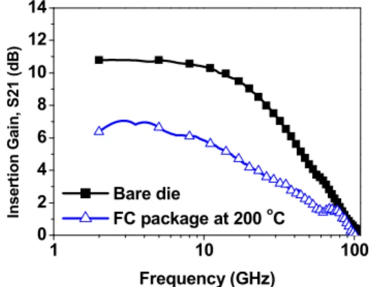
The IV characteristics before and after flip-chip assembly at the bonding temperature of 200 oC (for both the substrate and the device sides) are illustrated in Fig. 1. The drain current of the packaged device was slightly reduced as compared with the bare die data. The transconductance (gm) as a function of gate voltages was measured at a Vds of 0.8 V as depicted in Fig. 2. The gm
results presented match suite well before and after the assembly with the maximum value around 535 mS/mm. Fig. 3 shows on wafer S-parameter measurement results of the bare die and the flip-chip packaged device from 2 to 110 GHz. The measured insertion gain (S21) of flip-flip-chip packaged device decayed around 4 dB up to 30 GHz. The degradation of the package performance at high temperature bonding may be caused by thermomechanical stress due to large CTE mismatch between GaAs chip and RO 3210 substrate. Therefore, the bonding temperature of the substrate was reduced to 100 oC to avoid the performance degradation. Fig. 4 shows the RF performance of the packaged device at low temperature bonding of substrate under the same bias condition. The flip-chip packaged device showed less than 1 dB degradation up to 110 GHz as compared with the bare die data. The results demonstrate that flip chip package using organic
Nanotech Malaysia 2010: International Conference on Enabling Science and Nanotechnology, 8-10 December, 2010, KLCC, MALAYSIA
substrate can be used for nano scale mHEMT devices for high frequency applications with very small performance degradation up to 110 GHz.
Conclusion
The In0.52Al0.48As/In0.6Ga0.4As mHEMT was successfully fabricated on organic substrate by using
flip-chip technology. The poor performance of flip chip package showed 4 dB of reduction in insertion gain at high bonding temperature of 200 oC. In order to improve the performance of the packaged device, low bonding temperature at 100 oC was presented and obtained less than 1 dB degradation up to 60 GHz. Flip-chip bonding process at low temperature can effectively improve the performance of the package.
References:
[1]. T. Braun. “High Temperature Potential of Flip Chip Assemblies for Automotive Applications”, IEEE Electronic Components and Technology Conference, pp. 376-383, 2005. [2]. Myung Jin Yim. “Reduced Thermal Strain in Flip Chip Assembly on Organic Substrate using Low CTE Anisotropic Conductive Film”, IEEE Transaction on Electronics Packaging
Manufacturing, Vol. 23, No. 3, pp. 171-176, July 2000.
[3]. J. Tian. “Study of Thermal and Thermo-Mechanical Behavior in a Multi-chip-Composed Optoelectronic Package”, 9th Electronics Packaging Conference, pp. 886-891, 2007.
[4]. C. I. Kuo, et al., “InAs High electron Mobility Transistors with Buried Gate for Ultralow-Power-Consumption Low Noise Amplifier Application”, Japan Journal of Applied Physics, vol, 47, no. 9, pp. 7119-7121, 2008. 0.0 0.2 0.4 0.6 0.8 1.0 0 100 200 300 400 500 D ra in C u rr e n t ID ( m A /m m ) Drain-source Voltage VDS (V) Before FC After FC
Figure 1: The IV characteristics of mHEMT device before and after flip chip assembly.
100 200 300 400 500 600 in c u rr e n t (m A /m m ) 100 200 300 400 500 600 T ra n s c o n d u c ta n c e (m S 1 10 100 0 2 4 6 8 10 12 14 In s e rt io n G a in , S 2 1 ( d B ) Frequency (GHz) Bare die FC package at 200 oC
Figure 3: The measured S-parameter of flip chip packaged mHEMT device at high temperature bonding. 4 6 8 10 12 14 io n G a in , S 2 1 ( d B )
國科會補助計畫衍生研發成果推廣資料表
日期:2011/08/24國科會補助計畫
計畫名稱: 在矽基板整合40奈米三五族與鍺量子井場效電晶體作為低功率與高速無線之 應用(2/3) 計畫主持人: 張翼 計畫編號: 99-2120-M-009-005- 學門領域: 奈米電子光電技術研發成果名稱
(中文) 一種三五族半導體/高介電係數氧化層之表面處理方法 (英文)成果歸屬機構
國立交通大學發明人
(創作人)
張翼,張嘉華,林岳欽,金海光技術說明
(中文) 三五族(III-V)半導體由於具有高載子遷移率及高飽和速度,因此以III-V半導體 與高介電係數氧化層(high-k dielectrics)製作之場效電晶體具有極佳之轉導特 性、高截止頻率及較少的閘極延遲等優良特性。一般高介電係數氧化層需以沉積 的方式,沉積在三五族半導體上,作為閘極氧化層。然而,三五族半導體與沉積 之介電層的界面特性不良,容易形成極高界面缺陷密度(density of interface traps, Dit),因此在沉積之前採用表面處理技術,可降低介面缺陷。習知技術 大部分以三甲基鋁(trimethyl aluminum, TMA)或(NH4)2S+TMA做表面處理,本發 明提出以HCl整合TMA之表面處理方式,相較於傳統之表面處理方式,可以進一步 降低界面缺陷,減少電容頻率分散現象,並抑制閘極漏電流。(英文) This invention discloses a surface treatment method for the interface of III-V semiconductor/high-k dielectric. It includes pre-surface treatment by TMA on III-V semiconductors and chemical surface treatment after the high-k dielectric deposition.
產業別
研究發展服務業技術/產品應用範圍
邏輯電路、射頻元件技術移轉可行性及
預期效益
此方式可直接應用到台積電、聯電等IC產業,提升元件效能 註:本項研發成果若尚未申請專利,請勿揭露可申請專利之主要內容。99 年度專題研究計畫研究成果彙整表
計畫主持人:張翼 計畫編號: 99-2120-M-009-005-計畫名稱:在矽基板整合 40 奈米三五族與鍺量子井場效電晶體作為低功率與高速無線之應用(2/3) 量化 成果項目 實際已達成 數(被接受 或已發表) 預期總達成 數(含實際已 達成數) 本計畫實 際貢獻百 分比 單位 備 註 ( 質 化 說 明:如 數 個 計 畫 共 同 成 果、成 果 列 為 該 期 刊 之 封 面 故 事 ... 等) 期刊論文 15 15 100% 研究報告/技術報告 0 0 100% 研討會論文 7 7 100% 篇 論文著作 專書 1 1 100% 申請中件數 12 12 100% 專利 已獲得件數 0 0 100% 件 件數 0 0 100% 件 技術移轉 權利金 0 0 100% 千元 碩士生 4 4 100% 博士生 9 9 100% 博士後研究員 3 3 100% 國內 參與計畫人力 (本國籍) 專任助理 1 1 100% 人次 期刊論文 0 0 100% 研究報告/技術報告 0 0 100% 研討會論文 0 0 100% 篇 論文著作 專書 0 0 100% 章/本 申請中件數 0 0 100% 專利 已獲得件數 0 0 100% 件 件數 0 0 100% 件 技術移轉 權利金 0 0 100% 千元 碩士生 0 0 100% 博士生 0 0 100% 博士後研究員 0 0 100% 國外 參與計畫人力 (外國籍) 專任助理 0 0 100% 人次其他成果
(
無法以量化表達之成 果如辦理學術活動、獲 得獎項、重要國際合 作、研究成果國際影響 力及其他協助產業技 術發展之具體效益事 項等,請以文字敘述填 列。) International CooperationSupport-funding for students and researchers Interuniversity Microelectronic Center (IMEC) NTT Corporation
FBH IIT
Chalmers University of Technology
Tokyo Institute of Technology (Prof. Hiroshi Iwai &; Prof. Yasuyuki Miyamoto)
Fukui University self-funded
Dept. of Electric Engineering, Pennsylvania State University IHP
Dept. of Electric and Computer Engineering, Virginia Tech.
成果項目 量化 名稱或內容性質簡述 測驗工具(含質性與量性) 0 課程/模組 0 電腦及網路系統或工具 0 教材 0 舉辦之活動/競賽 0 研討會/工作坊 0 電子報、網站 0 科 教 處 計 畫 加 填 項 目 計畫成果推廣之參與(閱聽)人數 0