國
立
交
通
大
學
電子工程學系 電子研究所
博 士 論 文
新穎多閘極多晶矽奈米線薄膜電晶體之研製與其應用
Fabrication and Analysis of Novel Multiple-Gated Poly-Si Nanowire
Thin-Film Transistors and Their Applications
研 究 生:徐行徽
指導教授:林鴻志 教授
黃調元 教授
新穎多閘極多晶矽奈米線薄膜電晶體之研製與其應用
Fabrication and Analysis of Novel Multiple-Gated Poly-Si Nanowire
Thin-Film Transistors and Their Applications
研 究 生:徐行徽
Student:Hsing-Hui Hsu
指導教授:林鴻志
Advisors:Horng-Chih Lin
黃調元
Tiao-Yuan Huang
國 立 交 通 大 學
電子工程學系 電子研究所
博 士 論 文
A DissertationSubmitted to Department of Electronics Engineering and Institute of Electronics
College of Electrical and Computer Engineering National Chiao Tung University
in partial Fulfillment of the Requirements for the Degree of
Doctor of Philosophy in
Electronics Engineering
October 2011
Hsinchu, Taiwan, Republic of China
新穎多閘極多晶矽奈米線薄膜電晶體之研製與其應用
研究生:徐行徽
指導教授:林鴻志 教授
黃調元 教授
國立交通大學
電子工程學系 電子研究所
摘要
在本篇論文中,我們利用數種簡易的奈米線製備技術,製作並研究各式具 有多閘極結構的多晶矽奈米線薄膜電晶體。所提出的多閘極奈米線電晶體製備 方式包括"側壁邊襯蝕刻法(side-wall spacer etching)”與”空腔形成填充法(cavity formation and filling)”,使用此兩種製備方式均可免除昂貴的微影設備與製作技 術,自我對準形成各式高效能的多晶矽奈米線通道電晶體。 首先,我們針對使用側壁邊襯蝕刻技術所製作的雙獨立閘極多晶矽奈米線 電晶體,探討在不同操作模式下(雙閘或單閘)之元件特性。由於奈米線通道厚 度僅有約 10 奈米,強烈的閘極耦合效應(gate-to-gate coupling)會對元件電性造 成深切的影響。在雙閘操作模式下,此元件可達到小於 100mV/dec 之次臨限擺 幅(subthreshold swing);而在單閘模式下,利用閘極耦合效應來調整輔助閘偏壓 的方式可獲得不同的臨限電壓。實驗中我們也發現,在雙閘模式下由於不受背 閘極效應(back-gate effect)的影響,在輸出特性上會有比單閘操作高之飽和汲極 電壓,因此可獲得較大之飽和輸出電流(output saturation current);此外,在雙閘操作下對於通道中晶粒邊界與缺陷所造成之位能障 (grain-boundary potential barrier)具有較佳的調控能力,因而可獲得較單閘操作下為佳之元件特性。此發 現對於分析多晶矽通道元件之傳導機制具有重要的影響。我們也探討了雙獨立 閘極多晶矽奈米線電晶體的基本電性擾動分析。從實驗數據顯示,利用電漿處 理修補多晶矽通道裡的缺陷,可使元件之間的臨限電壓差異性降低,由此推測 出複晶矽奈米線通道中的缺陷密度與電性擾動有一密切的關聯性。另外,在不 同的操作模式下(雙閘或單閘),以雙閘極操作模式,可得到最小的臨限電壓標 準差。由於元件間通道厚度的差異所造成的臨限電壓擾動,會隨著橫跨在通道 薄膜之電場大小而不同;實驗中也證實,當在單閘操作模式下,控制閘極的固 定偏壓存在著一最佳值,能有效地降低臨限電壓的變異度。 除了使用側壁邊襯蝕刻法製作奈米線元件,我們也提出並發展了另一種新 穎的奈米線製備技術,稱作空腔形成填充法。利用此技術製作出的三閘極(tri-gate)多晶矽奈米線電晶體展現了相當陡峭的次臨限擺幅(~100mV/dec),和大於
108的開關電流比值(ON/OFF current ratio)。此結果驗證了多閘極可以有效增進 元件的效能。另外,一種基於空腔形成填充法,可以同時製作出具有不同閘極 結構但奈米線通道形狀相同之電晶體的製程技術也被提出。利用此簡單有趣的 製程,能有效分析與評估多重閘(Multi-gate)的實際效應,且有助於探討多重閘 對於奈米線元件的基本特性和及電性擾動的影響。實驗結果亦顯示越佳的閘極 控制能力對於奈米線元件之變異度也能越有效的控制。 在非揮發記憶體應用方面,我們利用空腔形成填充法成功地製作了多種閘 極型態的 SONOS 記憶體元件,包含單側閘極(side-gated, SG)、Ω 型閘(Ω-gated) 和全環繞閘極(gate-all-around, GAA)。其中全環繞閘極奈米線記憶體元件除了展 現出最佳的基本電性,記憶體特性方面包含寫入/抹除速度、電荷保持能力 (retention)和忍耐力(endurance)也具有很顯著的增進。這些實驗結果都歸因於全
控制能力。 在論文的最後部份,我們提出並製作一種具有延伸式感測閘(SENSE-gate) 與讀取閘(READ-gate)的新穎雙獨立閘極奈米線感測元件,並對於各種感測應用 的可行性進行初步的探討。此感測架構結合奈米線電晶體結構與延伸式閘極離 子感測場效電晶體(EGFET)的概念,可有效將元件操作區與充滿酸/鹼性化學物 質或生物分子溶液的感測區與隔離。因此所製作出之感測元件,同時具有延伸 式閘極感測元件之可靠度與系統整合能力,還有奈米線感測元件之優良的轉導 特性。此研究也呈現並討論各種實際感測的初步實驗結果,包括酸鹼感測(pH sensing)、生物分子偵測(bio-molecules detection)和氣體感測(gas sensing)。另外,
相較於把多晶矽奈米線直接曝露在環境中作感測的感測元件,此雙獨立閘感測 元件由於使用了延伸式閘極結構,在中性水溶液環境中的施壓測試(stressing testing)中明顯展現更穩定與可靠的電性結果。
關鍵字:奈米線, 多閘極, 多晶矽, 薄膜電晶體, 背閘極效應, 變異度, 非揮發記憶 體, SONOS, 感測器。
Fabrication and Analysis of Novel
Multiple-Gated Poly-Si Nanowire Thin-Film Transistors
and Their Applications
Student: Hsing-Hui Hsu
Advisors: Horng-Chih Lin
Tiao-Yuan Huang
Department of Electronics Engineering & Institute of Electronics
National Chiao-Tung University
Abstract
Various multiple-gated (MG) polycrystalline silicon nanowire (poly-Si NW)
thin-film transistors (TFTs) are fabricated and analyzed. The proposed NWTFT
schemes utilize very simple and low-cost NW preparation techniques, including
“side-wall spacer etching” and “cavity formation and filling”, to fabricate poly-Si NWs in a self-aligned manner. Detailed characteristics of the MG NWTFT devices
and their potential applications involving non-volatile memory (NVM) and chemical
sensors are also studied and demonstrated.
For NW devices fabricated by the side-wall spacer etching technique, the
characteristics of the poly-Si NWTFT featuring an independent double-gated (DG)
configuration are analyzed and compared. It is found that the device under DG mode
exhibits significantly better performance with respect to the two single-gated (SG)
and a smaller subthreshold swing (SS) of less than 100 mV/dec. Origins of such
improvement are identified to be due to the elimination of the back-gate effect as well
as an enhancement in the effective mobility with DG operation. The mobility
improvement in DG mode is ascribed to more efficient gate control in lowering the
grain-boundary potential barrier. Moreover, the VTH fluctuation behavior of poly-Si
NWTFTs is also investigated and studied. The defects existing in the NW channels are
identified as one of the major sources for the VTH fluctuation. The passivation of these
defects by plasma treatment is shown to be effective in reducing the VTH fluctuation.
It is also found that the fluctuation is closely related to the operation modes. When
only one of the gates is employed as the driving gate to control the device’s switching behavior, an optimum bias for the other gate could be found for minimizing the VTH
fluctuation.
On the development of new NW preparation method, the cavity formation and
filling technique is proposed, which enables the fabrication of poly-Si NW without
resorting to advanced lithographic tools. The tri-gated poly-Si NWTFTs built on this
novel technique show steep SS of around 100 mV/dec and ON/OFF current ratio
higher than 108, signifying the effectiveness of MG scheme in improving the device performance. Furthermore, a clever scheme based on cavity formation and filling
technique allowing fabricating test structures with identical NW channel but different
gate configurations is also proposed, and the impact of MG configurations on the
variation of NWTFTs characteristics is also investigated. The results show the
variation is reduced by increasing the portion of NW channel surface that is
modulated by the gate.
As regards NVM applications, we demonstrate the poly-Si NW-SONOS
having various gate configurations, namely, side-gated (SG), Ω-shaped gated (ΩG)
and gate-all-around (GAA), are successfully fabricated and characterized. The
experimental results show that much improved transfer characteristics are achieved
with the GAA devices as compared with the other types of devices. Moreover, GAA
devices also exhibit the best memory characteristics among all splits, including the
fastest P/E efficiency, largest memory window and best endurance/retention
characteristics.
Finally, the feasibility of the novel independent DG NW sensing device scheme
featuring an extended sensing gate (SENSE-gate) and a READ-gate for various
sensing applications is explored. This scheme takes advantages of extended-gate
ion-sensitive FET’s (EGFET) effective isolation of device from chemical and biological
environment, and NWFET’s good switching properties. The preliminary study using this novel sensing device for pH sensing, gas sensing and bio-molecules detection is
presented and described. In addition, owing to the use of extended-gate structure, this
novel sensing scheme exhibits more stable and reliable electrical characteristics
during the stressing test in aqueous solution as compared with those of NW sensor
devices having poly-Si NWs exposed to the ambient.
Keywords: Nanowire (NW), Multiple-Gate (MG), Polycrystalline Silicon (Poly-Si),
Thin-Film Transistor (TFT), Back-Gate Effect, Variability, Non-Volatile
Acknowledgement
首先要感謝指導教授林鴻志博士黃調元博士。林老師對研究的熱忱與觀念 的重視,和黃老師寬廣的眼界與嚴謹的態度使我在求學過程中獲益匪淺。老師 們的所有建議與話語都值得銘記在心,品味再三。 本論文的完成也要感謝口試委員—胡振國教授、楊裕雄教授、李佩雯教授、 崔秉鉞教授、簡昭欣教授、張睿達教授—所給予的寶貴建議與指導。 接下來要感謝的是所有曾為實驗室付出過的學長們:盧文泰博士、葉冠麟 博士、李耀仁博士、呂嘉裕博士、李明賢博士、林宏年博士、蘇俊榮博士、盧 景森博士、張伊鋒學長、李聰杰學長、藍文廷學長、林賢達學長,因為你們紮 下堅實的基礎,實驗室才能成長茁壯,生氣蓬勃。再來是碩班同期的夥伴們: 凱翔、志誠、雨霖、健銘、銑泓、振家、建松,雖然你們早已畢業,但是曾經 有過的情誼是無法被輕易抹滅的。感謝曾經一起努力打拼的博班夥伴:子儀、 哲民、嘉豪、政頤、克慧,還有碩士班的學弟妹:建富、子銘、大偉、忠祐、 文強、政雄、陳玲、冠樟、漢仲、君帆、瑄勻、格綸、佑寧、育嘉、政建、瑞 桀、維濤、家維、正偉、冠智、庭輔、冠宇、敏峰、段凱、歷樺、俊鵬、梵懿、 曉惠、維真、盈宇、庭耀、涵宇、等等,非常感謝你們除了在實驗上的協助與 貢獻,研究上與生活上的交流,也讓求學過程充滿樂趣。感謝生科系 LEPE 實 驗室的曉萍學妹、淵仁學長、蕭呈允博士在感測實驗上的幫忙,才能讓這本論 文順利的完成。特別感謝陳威臣博士,從實驗室大小事到一起在美國離鄉背井 相依為命,一路以來真的承蒙照顧,感激不盡。此外還要感謝 Dr. Charles Cheung 在 NIST 訪問研究期間的大力協助,讓我 能夠有這樣難得的機會去美國歷練。 感謝我所有生活上的朋友、夥伴,你們對於我的意義不是這本論文能夠比 擬的,你們在我生命中刻劃過的所有痕跡我都會永遠珍惜並且牢牢記得。 感謝我所敬愛的父母親徐敬業先生與邱小珍女士,感謝你們無微不至的照 顧與鼓勵,你們的養育之恩我一輩子也還不清;感謝姊姊徐行儷小姐常在重要 時刻分享寶貴的經驗;感謝細心可愛的禹伶陪我度過人生的高低潮,在美國也 互相扶持,一起突破困境,更一起累積了許多特別的經歷與回憶,感謝妳的陪 伴。 僅以此論文獻給摯愛的家人、朋友與敬重的師長。 徐 行 徽 誌於風城交大 2011 年 10 月
Contents
Abstract (Chinese)………i
Abstract (English)………iv
Acknowledgement………vii
Contents………viii
Table Captions………xii
Figure Captions………xiii
Chapter 1 Introduction………1
1-1 Overview of Nanowire Technology………1
1-2 Multiple-Gated Transistors………3
1-3 Variability of MOSFET Characteristics………4
1-4 Overview of Nonvolatile Memory………6
1-4.1 Charge-Trap Flash Memory………7
1-4.2 Nanowire Nonvolatile Memory………8
1-4.3 Three-Dimension Stackable Nonvolatile Memory………9
1-5 Overview of Solid-State Sensors………10
1-5.1 Ion-Sensitive Field-Effect Transistor………11
1-5.2 Nanowire Sensors………12
1-6 Motivation………13
1-7 Thesis Organizations………15
References………18
Chapter 2 Multiple-Gated Poly-Si Nanowire Thin-Film Transistors
Fabricated by Sidewall-Spacer Etching Technique……36
2-1 Introduction………36
2-2 Experimental………38
2-2.1 Device Structure and Fabrication………38
2-2.2 Electrical Characterization Methods and Measurement Setup……40
2-3 Basic Electrical Characteristics………41
2-3.2 Modulation of VTH with Back-Gate Bias………43
2-4 On the Origins of Performance Enhancement in Independent Double-Gated Poly-Si NWTFTs………46
2-4.1 Impacts of Back-Gate Effect on Device Performance………46
2-4.2 Investigation on Mobility Enhancement with Double-Gated……… Operation...………50
2-4.3 Impacts of Operation Modes on Series Resistance………52
2-5 Threshold Voltage Fluctuation of Independent Double-Gated Poly-Si……… NWTFTs………54
2-5.1 Theory of Threshold Voltage Fluctuation and Assumptions………54
2-5.2 Impacts of NH3 Plasma Treatment………57
2-5.3 Impacts of Operation Modes………59
2-6 Summary………61
References………63
Chapter 3 Multiple-Gated Poly-Si Nanowire Thin-Film Transistors
Fabricated by Cavity Formation & Filling Technique
………102
3-1 Introduction………102
3-2 Device Structures and Fabrication………104
3-2.1 Tri-Gated Poly-Si NWTFT………104
3-2.2 Poly-Si NWTFTs with Three Different Gate Configurations……105
3-3 Electrical Characteristics of Tri-Gated Poly-Si NWTFTs………107
3-4 Variability of Multiple-Gated Poly-Si NWTFTs………109
3-4.1 Impacts of Gate Configuration………109
3-4.2 Impacts of Multiple-Channel Configuration………111
3-5 Summary………112
References………113
Chapter 4 Impacts of Multiple-Gated Configuration on the
……
Characteristics of Poly-Si Nanowire SONOS Devices
……
………134
4-1 Introduction………134
4-2 Operation and Physical Mechanisms of SONOS-Type Nonvolatile Memory ………136
4-2.1 Program/Erase Operation Mechanisms………136
4-2.2 Reliability Mechanisms………138
4-3 Experimental of Poly-Si NW-SONOS Devices………140
4-3.1 Device Structures and Fabrication………140
4-3.2 Measurement Setup and Operation Principles………141
4-4 Basic Electrical Characteristics of Poly-Si NW-SONOS Devices………142
4-5 Programming/Erasing Characteristics………144 4-6 Reliability Characteristics………147 4-6.1 Endurance Characteristics………147 4-6.2 Retention Characteristics………150 4-7 Summary………151 References………153
Chapter 5 Poly-Si Nanowire Thin-Film Transistors Featuring an
…
Extended Sensing Pad for Sensor Applications………183
5-1 Introduction………183
5-2 Device Structure, Fabrication and Operation Principles………185
5-3 Experimental Setup for Sensing Purposes………187
5-3.1 Micro-Fluidic System and Measurement Settings………187
5-3.2 Immobilization of Bio-Molecules on Sensing Pad………188
5-3.3 Gas Chamber System and Measurement Settings………189
5-4 Poly-Si NW Sensing Device for Various Sensor Applications………190
5-4.1 Basic Electrical Characteristics of Poly-Si NW Sensing Devices ………190
5-4.2 pH Sensing………191
5-4.3 Bio-Molecules Detection………194
5-4.4 Gas Sensing………195
5-4.5 Robustness Test in Aqueous Environment………197
5-5 Summary………199
References………200
Chapter 6 Conclusions and Future Prospects………223
6-1 Conclusions………223
6-2.1 Crystallinity Improvement for Poly-Si NW………227
6-2.2 Gate Stack Engineering for NW-SONOS Devices………227
6-2.3 Three-Dimensional Integration for Poly-Si NWTFTs and NVMs ………228
6-2.4 Optimization of NWFET Sensing Devices………229
References………230
Vita………232
Table Captions
Chapter 2
TABLE 2-1 Definition of bias conditions for DG, SG1, and SG2 operation modes.………74
TABLE 2-2 Summary of equations for VTH-shift rate under different operation and
bias conditions from the theoretical model [2.13], and the experimental data.………81
Figure Captions
Chapter 1
Fig. 1-1 Schematic structures and energy band diagrams of planar single-gated MOSFET (left) and gate-all-around (GAA) NW MOSFET (right). Apparently the GAA NW structure can provide much better electrostatic control to prevent the lateral electric field penetrating from the drain into the channel region [1.25].………30
Fig. 1-2 Evolution of the new transistor structure to improve the electrostatics of a MOSFET [1.26].………30
Fig. 1-3 Schematics of conventional transistor with a top-mounted gate (left) and Intel’s tri-gate transistors with body-tied Si-fin structure (right) [1.28].…31 Fig. 1-4 Cross-sectional TEM images of gate-all-around twin silicon nanowire SONOS memory [1.54].………31
Fig. 1-5 Cross-sectional TEM images of (a) Tri-gate structure of the TFT device, (b) Channel-length direction of double-layer TFT NAND devices [1.60].…32
Fig. 1-6 Schematic cross-section of Toshiba’s BiCS flash memory (right) and its vertical SONOS cell (left) [1.62, 1.63].………32
Fig. 1-7 Schematic representation of (a) MOSFET and (b) ISFET [1.68].………33
Fig. 1-8 Table of ISFET, ChemFET and EnFET structures, detectable analytes, and sensitive membranes with bio-receptors [1.70].………33
Fig. 1-9 An illustrative representation of a sensor scheme built on extended gate field-effect transistor (EGFET).………34
Fig. 1-10 Size of several nano-materials as compared to the size of some biological entities, such as nucleic acids, proteins, virus, and cells [1.74].…………34
Fig. 1-11 Illustration of a reversible nanoscale biosensing process with NW sensor. (Left) A p-type silicon NW is functionalized with a receptor. (Center) Introduction of the appropriate ligand causes a change in NW conductance. (Right) NW conductance will return to its original value upon removal of the bound ligand, achieved by washing with buffer [1.78].………35
Chapter 2
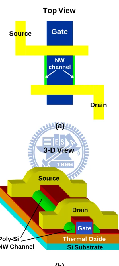
Fig. 2-1 (a) Top view and (b) 3-D structure of the novel poly-Si NWTFT featuring spacer-like NW channels and single side-gate configuration.………68
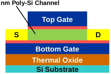
Fig. 2-2 (a) Top view and (b) 3-D structure of the poly-Si NWTFT with independent DG consisting of an inverse-T gate (G1) and a top gate (G2).…………69
Fig. 2-3 Key fabrication steps with schematic 3-D structure of the independent DG NWTFT. (a) Deposition of in situ doped n+ poly-Si. (b) Definition and formation of the inverse-T gate (G1). (c) Deposition of G1 oxide and poly-Si active layer. (d) Phosphorus ion (P31+) implantation. (e) Definition and
formation of source/drain (S/D) and NW channel by anisotropic etching. (f) Deposition of top gate (G2) oxide and definition of G2 to form the independent DG structure. (g) Schematic structure of the planar DG TFT with 50-nm-thick poly-Si channel.………70
Fig. 2-4 Cross-sectional TEM images showing the cross-section profile and dimensions of the fabricated NW channel.………73
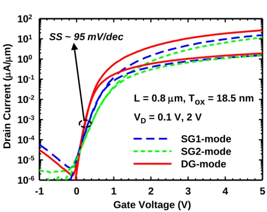
Fig. 2-5 Transfer characteristics under SG and DG modes of operations with L = 0.8
m. SG1 and SG2 refer to SG modes with G1 and G2 serving as the driving gate, respectively.………74
Fig. 2-6 (a) Schematic cross-sectional structure of the poly-Si DG-TFT used for TCAD simulation and (b) the designed S/D doping profile with a gradually decreased concentration from the top (ND ~ 5×1019 cm-3) to the bottom (ND
~ 1018 cm-3) of S/D regions.………75 Fig. 2-7 (a) Simulated ID-VG characteristics of the poly-Si DG-TFT structure shown
in Fig. 2-6 (a). (b) Simulated trap-assisted band-to-band tunneling (BTBT) generation rate inside the drain region at VG1 = VG2 = -2 V and VD = 3 V.
………75 Fig. 2-8 (a) Transfer characteristics of the NW device having G1 as the driving gate and G2 as the VTH-control gate. (b) Transfer characteristics of the planar
control device with TSi = 50 nm driven by the top-gate with bottom-gate as
the VTH-control gate.………76
Fig. 2-9 Schematics showing an independent DG MOSFET with its ID-VG
characteristics modulated by VTH-control gate for active- and
Fig. 2-10 The extracted VTH and SS as functions of VG2 for the NW device under
SG1 mode of operation. VTHDG denotes the VTH measured in DG mode.
………77 Fig. 2-11 Schematic potential distributions across the channel of an independent DG structure with ultra thin body for describing the relation between VTH-shift
rate and film thicknesses under different bias conditions [2.13].…………78
Fig. 2-12 Schematic potential distributions across the channel for describing the relation between SS and film thicknesses under different bias conditions [2.13].………79
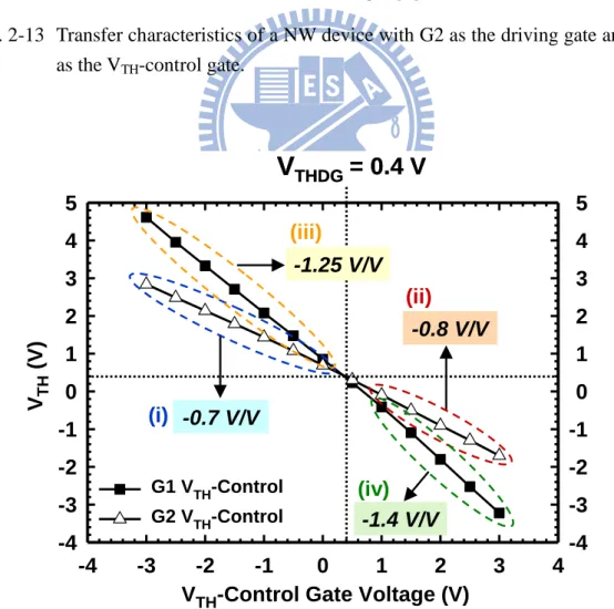
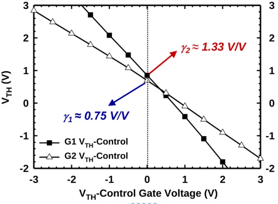
Fig. 2-13 Transfer characteristics of a NW device with G2 as the driving gate and G1 as the VTH-control gate.………80
Fig. 2-14 The extracted VTH as a function of VTH-control gate voltage. The values of
VTH-shift rate for the four operation regions are also indicated.…………80
Fig. 2-15 (a) Output characteristics of the NW device under different operation modes with L = 5 m. (b) Ratio of drain current of the DG mode to the sum of the two SG modes. VGVTH varies from 1 V to 5 V in step of 1 V.……82
Fig. 2-16 Energy band diagrams of DG structure with (a) thick channel and (b) thin channel. Dashed lines represent the distribution of inversion charges.…83
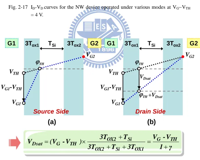
Fig. 2-17 ID-VD curves for the NW device operated under various modes at VGVTH
= 4 V.………84
Fig. 2-18 Schematic potential distribution for SG1-mode operation of the NW device at (a) source side and (b) drain side of the channel under pinch-off bias condition.………84
Fig. 2-19 Extraction of back-gate-effect factors for two SG modes at VTH-control
gate = 0 V.………85
Fig. 2-20 Comparisons of output characteristics between the measured data and calculated results of each operation mode based on the proposed model. ………86 Fig. 2-21 (a) GM of a NW device versus VG under different operation modes. The
arrows indicate the VTH. (b) Ratio of GM of the DG mode to the sum of the
two SG modes as a function of VGVTH. Results for the planar device are
Fig. 2-22 Normalized electron mobility as a function of VGVTH. 30% and 20%
mobility enhancement at respectively low and high VGVTH for DG mode
compared to SG modes are estimated.………88
Fig. 2-23 Extracted barrier height VB as a function of VGVTH for the NW device
operated under DG and SG modes.………89
Fig. 2-24 Ratios of GM and weighted eqVB/kBTof DG mode to the sum of two SG modes as a function of VGVTH.………89
Fig. 2-25 Schematic illustrations of local conductance distribution in NW channel and current flow through channel to S/D region under (a) SG mode and (b) DG mode.………90
Fig. 2-26 Estimated S/D resistance in (a) DG mode, (b) SG1 mode and (c) SG2 mode. The resistance was extracted from the ID-VD curves with various channel
lengths.………91
Fig. 2-27 Schematic expressions of equivalent resistance components under (a) SG mode and (b) DG mode.………92
Fig. 2-28 Extracted Rs ratio as a function of VGVTH. R’ is defined as the parallel
resistance of two Rs measured in each SG mode.………93
Fig. 2-29 Schematic illustration of electric field, E, as a function of depth x in the channel region of an MOSFET [2.27].………94
Fig. 2-30 Transfer characteristics under DG mode for poly-Si NW devices with NH3
plasma treatment. (a) ID in logarithmic scale. (b) ID in linear scale. 20
devices were characterized in the plot.………95
Fig. 2-31 Transfer characteristics under DG mode for poly-Si NW devices without NH3 plasma treatment. (a) ID in logarithmic scale. (b) ID in linear scale. 20
devices were characterized in the plot.………96
Fig. 2-32 Mean value and standard deviation of VTH as a function of channel length
for devices operated under DG mode.………97
Fig. 2-33 Standard deviation of VTH (VTH) as a functions of (LW)-1/2 for devices
with and without plasma treatment under DG mode of operation.………98
Fig. 2-34 Modified VTH as a functions of (LW)-1/2 by deducting the calculated value
of RDF model from Fig. 2-33.………98
devices with channel length of 2 m under three different operation modes. ………99 Fig. 2-36 VTH dependence on the poly-Si channel thickness: (a) single-gated devices
with partially depleted channel, (b) single-gated devices with fully depleted channel, and (c) double-gated devices with fully depleted channel [2.32]. ………100 Fig. 2-37 (a) Transfer characteristics of devices with channel length of 2 m measured by sweeping G1 voltage and fixed G2 bias ranging from -3 V to 3 V. (b) VTH as a function of top-gate bias for devices with different
channel length. 25 samples were characterized in each datum point.…101
Chapter 3
Fig. 3-1 (a) Top view and (b) 3-D structure of the tri-gated TFT device with poly-Si NW channels.………116
Fig. 3-2 Schematic process flow with 3-D structures of the tri-gated NWTFT. (a) Deposition of TEOS oxide and nitride dummy layers on a Si substrate capped with a thermal oxide. (b) Formation of cavities by selective wet etching of the TEOS oxide. (c) Phosphorus ion (P31+) implantation. (d)
Definition and formation of source/drain (S/D) and NW channels by an anisotropic etching. (e) Removal of nitride hard-mask and TEOS dummy layers by a 2-step selective wet etching. (f) Deposition of gate oxide and formation of poly gate electrode.………117
Fig. 3-3 Cross-sectional TEM images of the tri-gated NWTFT.………120
Fig. 3-4 Key steps for fabricating NWTFTs with various gate configurations. (a) Patterning nitride hard-mask by anisotropic reactive plasma etching. (b) Formation of undercut (cavity) by selective wet etching TEOS dummy layer. (c) a-Si deposition and annealing, and S/D implant. (d-1) Definition and formation of S/D and NW channel by anisotropic etching. (d-2) Nitride removal with hot H3PO4. (d-3) TEOS removal by DHF. (e-1 to e-3)
Deposition of gate oxide and formation of poly gate for three types of NW devices (S1, S2 and S3).………121
Fig. 3-5 Cross-sectional TEM images of (a) S2 and (b) S3 NWTFTs.…………122
Fig. 3-6 Transfer characteristics of tri-gated NWTFT with L = 0.4 m and 5 m. ………123 Fig. 3-7 Output characteristics of tri-gated NWTFT with (a) L = 0.4 m and (b) L =
5 m.………124
Fig. 3-8 Layout of an NWTFT with multiple channels. In this example, the number of channel is 18.………125
Fig. 3-9 Transfer characteristics of tri-gated NWTFT with various NW channel numbers.………125
Fig. 3-10 Normalized drain current and subthreshold swing (SS) of NWTFTs as a function of channel number.………126
Fig. 3-11 Transfer characteristics of S1, S2, and S3 NWTFTs with L = 2 m.……126 Fig. 3-12 Mean value and standard deviation of SS of NWTFTs with (a) L = 0.7 m and (b) L = 5 m. 20 samples were characterized for each device condition. ………127 Fig. 3-13 Mean and standard deviation of threshold voltage (VTH) of NWTFTs with
(a) L = 0.7 m and (b) L = 5 m. 20 samples were characterized for each device condition.………128
Fig. 3-14 Standard deviations of VTH (VTH) as a function of (LW)-1/2 for both planar
and NW TFTs.………129
Fig. 3-15 Transfer characteristics of NWTFTs with S3 structure for channel number of (a) 2, (b) 6, (c) 50, and (d) 100. The channel length is 0.7 m. 20 samples were characterized in each figure.………130
Fig. 3-16 Mean value and standard deviation of (a) VTH and (b) SS for S3 devices of
various channel numbers.………132
Fig. 3-17 VTH as a function of (LWeff)-1/2 for S3 devices of various channel numbers.
Chapter 4
Fig. 4-1 (a) Schematic structure of a conventional n-type SONOS memory device. (b) Influence of trapped charges on VTH of the SONOS memory device.
………158 Fig. 4-2 Energy band diagrams of SONOS structures in (a) flat-band, (b) positive gate bias (programming), and (c) negative bias (erasing) conditions.…159
Fig. 4-3 Energy band diagrams illustrating the injection of electrons from Si substrate to nitride via (a) FN tunneling and (b) direct tunneling.………160
Fig. 4-4 Energy band diagram of BBHC injection at the drain side of an nMOSFET. ………160 Fig. 4-5 Band diagram showing the charge loss paths in SONOS: thermal excitation (TE), Frenkel-Poole emission (FP), band tunneling (TB), trap-to-trap tunneling (T-T), and band-to-trap-to-trap tunneling [4.19].………161
Fig. 4-6 Process flow for the fabrication of the three types of poly-Si NW devices with various gate configurations. (a) Deposition of nitride/TEOS oxide/nitride dummy layers on a Si substrate capped with buried oxide. (b) Patterning a dummy structure by anisotropic reactive plasma etching and formation of cavities by selective wet etching of the TEOS oxide. (c) a-Si deposition and annealing for crystallization, and S/D implant. (d-1) Definition and formation of S/D and NW channel by anisotropic etching. (d-2) Nitride and TEOS oxide removal with hot H3PO4 and DHF,
respectively. (d-3) Bottom nitride removal by hot H3PO4. (e-1 to e-3)
Deposition of ONO stack and formation of poly gate for three types of NW-SONOS devices (SG, ΩG and GAA).………162
Fig. 4-7 Cross-sectional TEM images of the fabricated devices with (a) SG, (B) ΩG, and (c) GAA configurations.………165
Fig. 4-8 Schematic process flow for the simultaneous fabrication of the planar and GAA NW SONOS devices.………166
Fig. 4-9 Schematic illustration of measurement setup.………167
Fig. 4-10 Comparisons of transfer characteristics of the three types of poly-Si NW-SONOS and planar TFT-NW-SONOS devices.………168
Fig. 4-12 (a) Programming and (b) erasing characteristics of the ΩG devices.……170
Fig. 4-13 (a) Programming and (b) erasing characteristics of the GAA devices.…171
Fig. 4-14 Comparisons of P/E speed for three types of poly-Si NW-SONOS devices with (a) VG = 11 V, (b) VG = 13 V and (c) VG = -10 V.………172
Fig. 4-15 Simulated electric field distribution (left) along the paths indicated by the arrows shown in the 2-D simulation profiles (right) of SG and GAA devices.………173
Fig. 4-16 Simulated electric field along channel-width direction (Y-direction) in the oxide at two locations, X1 (near channel surface, solid line) and X2 (near gate, dot line), for a SG device.………174
Fig. 4-17 Fresh, programmed, and erased subthreshold characteristics of (a) SG, (b) ΩG, and (c) GAA devices.………175 Fig. 4-18 Endurance characteristics of (a) SG, (b) ΩG, and (c) GAA devices.……176
Fig. 4-19 (a) Subthreshold and (b) transconductance (GM) characteristics of a SG device after one, 1k, and 10k P/E cycles of operation.………177
Fig. 4-20 Subthreshold characteristics of (a) ΩG and (b) GAA devices after one, 1k, and 10k P/E cycles of operation.………178
Fig. 4-21 GM characteristics of (a) ΩG and (b) GAA devices after one, 1k, and 10k P/E cycles of operation.………179
Fig. 4-22 Subthreshold swing (SS) as a function of P/E cycles for the three splits of NW devices.………180
Fig. 4-23 Retention characteristics of (a) SG, (b) ΩG and (c) GAA devices at room temperature (25 ºC) after single and 10k P/E cycles of operation.……181
Fig. 4-24 Retention characteristics of GAA devices at 85 ºC after single and 10k P/E cycles of operation.………182
Chapter 5
Fig. 5-1 (a) Top view and (b) cross-sectional view of the novel poly-Si NWFET sensing device featuring extended sensing pads and independent double-gated (DG) configuration.………203
Fig. 5-2 Process flow in layout views for fabrication of the DG NWFET sensing devices with extended sensing pads. (a) Formation of an inverse-T gate. (b) Definition and formation of S/D and NW channel by anisotropic etching. (c) Deposition of G2 oxide and n+ poly-Si, followed by definition of G2 (SENSE-gate). (d) Formation of contact holes. (e) Metallization and formation of sensing pads and Al2O3 sensing membrane.………204
Fig. 5-3 Schematic illustration of the micro-fluidic channel system.………205
Fig. 5-4 Pictures of the components of the micro-fluidic channel system. (a) The chip holder. (b) The flexible micro-fluidic channel made of PDMS. (c) The acrylic mold.………206
Fig. 5-5 Pneumatic micro-pump with an injector used for injecting the sample solution into the micro-fluidic channel.………207
Fig. 5-6 (a) Cross-sectional view and (b) top view of the sensor chip equipped with the micro-fluid channel system.………207
Fig. 5-7 (a) Structural formula of APTES. (b) Schematic diagram of APTES immobilized on the Al2O3 sensing membrane.………208
Fig. 5-8 Schematic diagram of immobilization process and detection of DNA-hybridization.………208
Fig. 5-9 Photographs of (a) the capped sensing chamber and (b) uncapped gas-sensing chamber.………209
Fig. 5-10 Transfer characteristics of fabricated DG poly-Si NWFET sensing devices (a) without and (b) with 2-hr NH3 plasma treatment.………210
Fig. 5-11 (a) ID-VG characteristics of the DG poly-Si NWFET sensing device under
SG1 mode with G2 bias ranging from -2 V to 2 V. (b) VTHG1 as a function
of VG2 extracted from Fig. 5-11(a).………211
Fig. 5-12 S ch e m a t i c r ep r e se nt at i on o f si t e - bi n di n g m od el s ho wi n g t h e binding/dissociating reaction between the binding sites and protons on the
sensing surface under different pH values.………212
Fig. 5-13 Schematic representation of Gouy-Chapman-Stern (GCS) double layer model [5.15].………213
Fig. 5-14 Real-time ID response of a DG NWFET sensor measured in the test
solution with various pH values.………214
Fig. 5-15 (a) Subthreshold characteristics and (b) the corresponding VTH of the DG
NWFET sensor at corresponding pH values.………215
Fig. 5-16 Real-time biosensing characteristics of the DG NWFET sensor with sensing membrane surface modified by CA16 DNA probes.…………216
Fig. 5-17 Real-time ID response measured under various gas conditions in the gas
chamber.………217
Fig. 5-18 Schematic showing an ssDNA droplet dripped onto the sensing pad of a DG NWFET sensor.………217
Fig. 5-19 Real-time ID response to the condition of gas chamber using a sensing
device with ssDNA targeting layer.………218
Fig. 5-20 Real-time ID response to the condition of gas chamber using the device
tested in Fig. 5-19 after removing the attached ssDNA by DIW cleaning. ………218 Fig. 5-21 ID-VG curves ((a) with ID in logarithmic scale and (b) with ID in linear scale)
of a DG-NW sensor measured after corresponding stressing time. The stressing tests are performed by immersing the sensing region of the device in PBS (pH = 7) with micro-fluidic channel system and biased at VD = VS =
VG = 0 V.………219
Fig. 5-22 ID-VG curves ((a) with ID in logarithmic scale and (b) with ID in linear scale)
of ex-NW sensor measured after corresponding stressing time.………220
Fig. 5-23 Extracted VTH shift (ΔVTH) of (a) DG-NW sensor and (b) ex-NW sensor as
a function of stressing time.………221
Fig. 5-24 ON-current variation (ΔION) of (a) DG-NW sensor and (b) ex-NW sensor
Chapter 1
Introduction
1-1 Overview of Nanowire Technology
In the past two decades, the field of nanotechnology has been vastly explored
and investigated. The study of nanotechnology involves diverse topics, including
material science, biological science, atomic- and molecular-scale physics, electronics
engineering, etc. In terms of the usefulness and potential applications of
nanotechnology, some novel nanostructures, such as nanowire (NW), have received
particular attention and regarded as a promising choice for future electronics due to
their desirable features as well as progressively improved fabrication techniques for
pragmatic development and production purposes.
An NW is defined as a stripe-shaped material with a diameter or feature size
smaller than 100 nm. For this kind of structure, the ratio of the surface area to volume
increases as its cross-sectional dimensions shrink. Accordingly, NW can achieve a
very large surface-to-volume ratio from its tiny volume, giving rise to a significant
impact of the surface condition on material properties and carrier transport. Owning to
this inherent property, semiconductor NWs are attractive to a variety of electronic
applications, such as nano CMOS [1.1], NW TFTs [1.2], memory devices [1.3], and
sensors [1.4]. For a field-effect transistor (FET), using NWs as the channel enables
off-state leakage current to realize high performance and fast switching property. For
memory applications, memory devices built on NW structure possess high
programming/erasing (P/E) efficiency and low-voltage operation [1.5]. For sensor
applications, NW‟s high surface-to-volume ratio is conducive to high sensitivity to the
target under detection [1.6].
In general, the preparation methods of NWs can be classified into two groups,
one is “top-down” and the other one is “bottom-up”. In top-down methods, advanced
lithography tools, like deep-UV [1.1], e-beam [1.7] and nano-imprint [1.8], are
usually essential to generate NW patterns. With its capability of precise positioning
and good reproducibility, this approach is suitable for mass production. Currently
nano-scale lines down to or even narrower than 30 nm are routinely generated in
production lines to fabricate advanced circuitries with high yield. However, the
mature processing techniques still face certain issues. For example, the fabrication
cost is extremely high as costly exposure apparatus or expensive materials like
silicon-on-insulator (SOI) are used. Moreover, the process usually requires
cutting-edge technology. Therefore, it is hard to be employed popularly in academia such as
university for research purpose. Besides, the selection of NW materials is quite
inflexible because of the limitation set by the substrate material. Some alternative
top-down approaches using relatively cheap conventional photolithography tools (e.g.,
G-line and I-G-line steppers) with unique process techniques, such as thermal flow [1.9],
chemical shrink [1.10] and spacer patterning [1.11], have also demonstrated their
ability of fabricating NW devices. Nevertheless, these methods are not able to
generate NW patterns directly, and hence require more complex processing
procedures.
the capability of synthesizing NW with various kinds of materials [1.12]. Methods
categorized under bottom-up approach include metal-catalyzed vapor-liquid-solid
(VLS) [1.13], solid-liquid-solid (SLS) [1.14], solid-phase-diffusion [1.15], molecular
beam epitaxy (MBE) [1.16], oxide-assisted growth [1.17], and so forth. Among these
diverse techniques, the most successful and prevalent one is the VLS method because
of its flexible and simple preparation procedure. VLS method offers a more
economical and affordable option to fabricate NWs, greatly facilitating the related
researches in academia. Although bottom-up methods are remarkably cheaper than
top-down methods and more flexible for experimental purpose, they have their own
shortcomings. First, length, diameter and orientation of NWs are not easy to be
controlled precisely. The prepared NWs are difficult to be aligned and positioned
accurately, especially for the purpose of device fabrication. For metal-catalyzed
growth, metal contamination is also a potential concern. Furthermore, the formation
of reliable contacts for electrodes reveals another challenging issue.
1-2 Multiple-Gated Transistors
In the challenges of shrinking devices to nanometer scale, one critical obstacle
is how to increase the gate controllability over the channel in order to suppress the
short-channel effects (SCEs), which stem from the lateral electric field penetrating
from the drain into the channel region and thus weakens the gate control [1.18].
Reduction of gate oxide thickness could provide some help, but may also dramatically
increase the tunneling current from gate electrode and then aggravate the power
controllability are feasible; one is applying high-κ materials as gate insulator in place
of conventional SiO2, and the other is adopting a multiple-gated (MG) configuration.
A number of MG device schemes have been proposed so far [1.19-1.24]. In
comparison with single-gated device, MG structure can provide much better
electrostatic control over the channel region to mitigate SCEs, as shown in Fig. 1
[1.25]. Among the innovations of MG devices, quasi planar FinFET has already
drawn a lot of attention in the past decade [1.20, 1-21]. The FinFET structure is able
not only to perform double-gated or tri-gated control, but also to have good ability to
shrink the channel dimension into nano-meter scale. Moreover, owing to its
quasi-planar structure, FinFET is versatile to be incorporated into modern fabrication
processes. Several types of FinFET structures have been proposed and evolved (as
shown in Fig. 2 [1.26]), including double-gate (DG) (UC Berkeley) [1.21], tri-gate
(Intel) [1.22], Ω-gate (TSMC) [1.23], etc. The most ideal and ultimate MG
configuration is gate-all-around (GAA) NW structure [1.24], which exhibits the best
gate controllability over the channel potential. In addition, with moderate size of NW,
the quantum mechanical effects existing in quasi-1D NW channel could benefit
carrier transport properties in terms of lower scattering rate and higher ballistic
efficiency [1.27]. In mid-2011, Intel has announced that the tri-gated body-tied Si-fin
structure (on the right of Fig. 3) will be used as the building block on the company's
next 22 nm-generation chips [1.28].
1-3 Variability of MOSFETs Characteristics
operation voltage to retain acceptable reliability and power dissipation [1.29].
Nevertheless, the functionality of circuits and individual electrical properties of
advanced CMOS devices become more sensitive to the device structural parameters
as well as process variations during the fabrication [1.30]. Threshold voltage (VTH)
fluctuation in MOSFETs has been regarded as one of the most difficult challenges for
further down-scaling [1.31]. This fluctuation is originated from a plethora of variation
sources, including patterning proximity effects [1.32], line-edge roughness due to
lithographic and etching [1.33], thin-film variation (thickness variation [1.34], defects
and fix charges [1.35]), the granularity of gate material [1.36, 1.37], strain process
variation [1.38], and random dopant fluctuation (RDF) [1.39, 1.40].
It has been shown that RDF plays an increasingly pronounced role in VTH
fluctuation in extremely scaled MOSFETs [1.41]. RDF means the fluctuation caused
by randomly scattered spatial distribution of impurity atoms in the channel of devices.
Since the ion implantation and diffusion processes for doping are unable to control the
exact number of dopants and precisely locate them individually, RDF is an inevitable
phenomenon in conventional MOSFET scheme. In a 50 cubic nanometer volume with
doping concentration of 1018 cm-3, there are only 125 dopants in this space. Therefore, the variation of dopant number in the depletion region would result in a considerable
difference in VTH. Consequently, it is imperative to find out a suitable solution or
strategy to circumvent this intrinsic problem while device dimensions keep shrinking.
Fully depleted SOI (FD-SOI) and MG schemes might be possible solutions to deal
with this problem [1.42]. Owing to their enhanced gate controllability and immunity
to SCEs, the channel doping formerly used to prevent SCEs in conventional
MOSFETs can be relieved and remain undoped to eliminate the part of VTH
1-4 Overview of Nonvolatile Memory
Driven by the unceasing reduction of cost and increase of memory density, the
market of nonvolatile memory (NVM) has been growing rapidly over the last two
decades. “Non-volatile” indicates that a memory device can retain stored data even if
the power is switched off. This feature enables more convenient data access and
therefore ideally suitable for portable electronic products. One of the most important
inventions in NVMs is flash memory [1.43], which possesses a number of advantages
such as byte-selectable write operation combined with sector “flash” erase,
non-volatility, good durability and low power. Therefore it becomes the most ideal choice
for data storage in numerous electronic systems.
At present, the most prevailing cell device structure for flash memory is the
floating-gate device. However, as the memory cell keeps shrinking, the floating-gate
device is confronted by several scaling limits. Since the storage layer is made of
poly-silicon, the narrow spacing between two adjacent memory cells would lead to
coupling interference, resulting in undesirable threshold voltage shift and data
disturbance [1.44]. Another issue is associated with the scaling of tunnel oxide
thickness which is essential for low P/E operation voltages. For a thin dielectric, the
stress-induced leakage current (SILC) may cause all charges stored in the conductive
floating gate to leak out, thus degrading the reliability of memory devices [1.45]. This
limits the thickness of tunneling oxide at around only 7 nm. Although the multi-level
cell (MLC) technique has been applied in real products to increase memory capacity
per cell [1.46], the number of charges needed for differentiating storage levels is down
to tens of electrons in a sub 30 nm node flash, giving rise to a large variation in
memory window and aggravated interference between cells [1.47]. Consequently,
planar NAND flash technology at around the 10 nm node [1.48]. In addition, below
the 20 nm technology node, 3-D NAND flash will be a likely solution to increase the
memory density without aggressively reducing the feature size of memory devices
[1.48].
1-4.1 Charge-Trapping Flash Memory
To address the aforementioned problems met in conventional floating-gate flash
technology, the most likely candidate is the charge-trapping flash (CTF) memory
[1.49]. Silicon-oxide-nitride-oxide-Silicon (SONOS) multi-layer scheme has been
widely studied and reported in CTF device technology [1.50]. For a SONOS device,
each layer of the ONO dielectric stack, namely, oxide tunneling layer, nitride trapping
layer and oxide blocking layer, represents distinct function for memory operation.
Unlike conventional floating-gate flash device, CTF-type device normally uses an
insulator (e.g., Si3N4) or discrete nano-crystals (e.g. metal nano-dots [1.51]) in place
of the floating gate as the charge storage layer, so that the charges can be discretely
stored and isolated by deep-energy-level trapping centers in the trapping layer.
Therefore, CTF memory devices not only effectively minimize cell to cell coupling
interference, but also exhibit much stronger immunity against charge leaking through
a single defect formed in the tunneling oxide, hence improving the data retention.
Recently, some advanced multi-layer structures have been conducted to replace
SONOS for further improving the performance of CTF devices, such as TANOS
(TaN/Al2O3/Nitride/SiO2/Si) structure proposed by Samsung [1.52] and band-gap
engineered SONOS (BE-SONOS) proposed by Macronix [1.53]. In the TANOS
structure, a high-Al2O3 dielectric which has an energy barrier comparable to that of
coupling ratio, thus enhancing the electric field in tunneling oxide under P/E
operation while maintaining adequate retention characteristics with thick enough
blocking and tunneling layers. Besides, the high-work-function TaN gate material can
effectively suppress gate-injection current during erase operation due to the higher
energy barrier seen by the electrons in the gate, leading to a better erasing efficiency.
In BE-SONOS, the conventional SiO2 tunneling layer is replaced by an ultra-thin
ONO multi-layer. With proper band-gap engineering, this tunneling layer structure
can provide thick energy barrier to restrain direct tunneling at low electric field during
retention. While during erase operation, the tunneling barrier becomes ultrathin due to
a suitable band offset at high electric field, allowing efficient hole direct tunneling for
fast erasing.
1-4.2 Nanowire Nonvolatile Memory
Silicon NW (SiNW) has a great potential to shrink memory cells to nano-meter
scale without suffering from short-channel effects (SCEs). Furthermore, due to the
inherently large surface-to-volume ratio, electric potential in NW channel is very
sensitive to the surface condition. By utilizing this property to nonvolatile memory, a
smaller amount of charge storage could cause a larger threshold voltage shift of
memory device to obtain sufficient memory window. In addition, for a SONOS device
with a cylindrical NW channel and gate-all-around (GAA) configuration (as shown in
Fig. 4 [1.54]), the electric field at the channel-to-gate dielectric interface can be
enlarged compared to that of planar devices, hence P/E time or voltage could be
dramatically reduced [1.54]. At present, the proposed concepts and techniques for NW
NVM include SONOS [1.55], FRAM [1.56], nano-dot [1.57], molecule-gate [1.58],
to those of the flash memory nowadays. SONOS and FRAM can be built on the
development experience of planar devices, relatively feasible for NW NVM
applications in the near future.
1-4.3 Three-Dimensional Stackable Nonvolatile Memory
With respect to high-density memory applications such as NAND flash,
currently many studies have been devoted to exploring alternative approaches to deal
with the forthcoming physical scaling limit of memory devices. The most apparent
way is to increase memory cell density in vertical dimension, i.e. 3-D memory.
Samsung has reported a 3-D stacked NAND flash array with double single-crystalline
Si (Si) layer [1.59]. However, in this approach it is difficult to further stack more
c-Si layers on their inter-layer-dielectric (ILD) because of more and more rigorous
thermal budget and thin-film quality control. At the expense of transistor performance,
using poly-Si thin-film-transistor (TFT) as SONOS device would be much easier to
stack memory arrays vertically for 3-D configuration due to the relatively low process
temperature (Fig. 5) [1.60, 1.61]. An even more sophisticated 3-D NVM array
architecture called Bit-Cost Scalable (BiCS) flash has been proposed by Toshiba (Fig.
6) [1.62, 1.63]. The NAND strings in BiCS scheme consist of vertical poly-Si
TFT-SONOS pillars and multi-layer electrodes. This novel 3-D NVM scheme allows much
more increased device density without aggressively reducing device size, and also
1-5 Overview of Solid-State Sensors
Solid-state sensor is a sensor device made of solid-state material (e.g., silicon),
which is able to detect and respond to physical or chemical stimuli, and then convert
the input signal into a suitable output (e.g., electrical response) to be transferred to an
actuator for actuating, or a monitor for observing. Based on the properties of the
object to be sensed, sensor devices can be classified into three types. The first one is
physical sensor for measuring physical characteristics such as mass, distance,
temperature, etc [1.64]. The second one is chemical sensor for detecting chemical
substances according to their chemical or physical responses [1.65]. The last one is
biosensor for identifying particular biological substances by using a modified sensor
device with biological sensing interface [1.66].
Since the first ion sensitive field effect transistor (ISFET) introduced by P.
Bergveld in 1970 [1.67], solid-state sensors based on semiconductor devices have
attracted a substantial attention. Owing to their capability of miniaturization and
compatibility with modern VLSI processes, numerous advantages could be obtained
in terms of low cost, standardization, mass production, and applicability for simple
testing equipment. Moreover, by integrating miniature sensors with microelectronic
circuit, the performance of the so-called integrated sensors can be further improved.
These features make semiconductor-based sensors a favorable choice for medical
applications.
Two of the most prominent innovations for chemical and biological sensor
1-5.1 Ion-sensitive Field-Effect Transistor
In brief, Ion-sensitive field-effect transistor (ISFET) is a sensor device
combined with electrochemistry and microelectronics, featuring an ion-selective
electrode together with the traits of FET. The configuration and working principle of
ISFETs are quite similar to those of conventional MOSFETs, except the gate electrode
is generally replaced by an electrolytic solution with a reference electrode inserted, as
shown in Fig. 7 [1.68]. Therefore, the gate dielectric or the sensing membrane on top
of the channel of the ISFET is directly exposed to the solution to serve as a receptor
with its surface dangling bonds (binding sites), enabling the binding reaction with
target ions (e.g., H+) in electrolyte to determine the electric potential of the chemical gate [1.68]. Consequently, alterations in electrolyte such as the species of ions or ion
concentration can vary the potential of the chemical gate, so that the sensing operation
can be achieved by detecting either the threshold voltage shift or the drain current
change of the ISFET modulated by the field-effect mechanism.
Compared to the traditional glass ion-selective electrode, ISFET possesses
several distinctive merits, including compactness, compatibility with standard CMOS
process, high input and low output impedances, high durability, measurability with
small volume of sample, faster response, etc. In addition to ion selective sensing,
ISFET modified with an immobilized enzyme as sensing membrane can be
functionalized to serve as an enzyme selective sensor, called enzyme-modified FET
(ENFET) [1.69]. Various applications of ISFET and its derivatives, as well as the
detectable analytes are shown in Fig. 8 [1.70]. While dealing with the invasive
chemical solution or biological environment, another commonly-used ISFET-type
sensor is extended gate field-effect transistor (EGFET) [1.71]. In this configuration,
extended conduction wire connected to the gate electrode of FET (as shown in Fig. 9),
so that the active region of FET can be isolated from the invasive environment during
operation. Moreover, the EGFET structure is insensitive to noises caused by light and
temperature, and provides good flexibility for selecting suitable membranes for
different targets as well as the shape of extended gate, thus simpler passivation and
encapsulation for packaging can be achieved.
1-5.2 Nanowire Sensors
In recent years, one dimensional (1-D) nanostructures such as NWs for sensor
applications have attracted considerable research interests, especially for
bio-molecular sensing because of the stringent requirements for ultra-sensitive detection
with low-level molecular concentration [1.66, 1.72]. For a conventional ISFET-based
biosensor, the exposed sensing area of device channel is exceedingly larger than
molecular dimensions, necessitating a great amount of molecules to be bound to the
sensing membrane in order to create a sufficient potential change of the chemical gate,
and therefore the sensitivity and response time for low-level detection are greatly
impeded.
NW biosensors have shown desirable potential for overcoming many obstacles
encountered by current ISFET biosensor technologies [1.4, 1.73]. Since NW features
high surface-to-volume ratio and its critical dimensions are comparable to the size of
biological molecules, such as proteins and nucleic acids (as shown in Fig. 10 [1.74]),
any interaction between NW‟s surface and charged molecules in the testing
environment may provoke significant changes in electrical properties of the NW
device, enabling ultra-sensitive, real-time and direct (i.e., label-free) sensing
concentrations of proteins [1.75], DNA [1.76] and single virus [1.77] has been
demonstrated by using silicon NW. Fig. 11 illustrates a reversible nanoscale
biosensing process with an NW sensor [1.78].
However, using measurement approaches which directly immerse NW sensor in
a test solution during testing could drastically affect the reliability of the sensor device
and precision of the measurement results. Besides, it is difficult to preserve the NW
devices for a long time without solid passivation, hence hindering the realization of
practical production.
1-6 Motivation
Since Si NWs are attractive to various applications and have potential to be an
ideal building block for future electronics, pursuing a more reliable and
high-performance NW device as well as developing more feasible fabrication processes are
imperative and worthy of studying. To address the issues encountered in typical
top-down and bottom-up approaches for NW device fabrication as introduced in Sec. 1-1,
our laboratory (ADT Lab) has proposed and developed a novel poly-Si NW
field-effect transistor scheme which cleverly employs the sidewall spacer etching technique
to define poly-Si NWs channels and features a single side-gate structure [1.79, 1.80].
This scheme offers the following advantages: (1) Simple and low-cost fabrication
process, (2) controllable NW‟s size, (3) accurate positioning and self-aligned
source/drain and NW formation, (4) more reliable formation of contact, and (5) easy
to integrated with CMOS processes.
device performance compared to the planar counterparts in our previous works,
including reduced short channel effects (SCEs) and steeper subthreshold swing (SS).
Nonetheless, the ON current and gate controllability of this NW device are limited by
the small conducting width inherent with the single side-gated structure. Another
major concern associated with this scheme is the use of poly-Si NWs as the channel
material. Defects contained in the granular poly-Si channel are known to hinder
carrier transport and provoke undesirable leakage current, leading to deteriorated
ON-state current drive as well as switching properties of the devices.
Several ways are possible to alleviate these concerns. One is to improve the
film crystallinity by implementing available process schemes such as metal-induced
lateral crystallization (MILC) [1-81]. An alternative strategy is the adoption of MG
configuration, which is expected to further improve the performance of poly-Si
NWTFT devices through an increase in the effective channel width and enhanced gate
controllability over the channel. In addition, the MG configuration can be designed to
consist of several separate gates, and each gate can be biased independently, enabling
more freedoms for device operation.
For NVM application, some challenging issues existing in conventional TFT
memory devices, such as poor SS and large leakage current, which would require high
voltages for P/E operations and raise the power dissipation. By adopting poly-Si NW
channel with a MG configuration, these problems could be mitigated.
For sensor application, to cope with the obstacles met in conventional ISFET
and NW sensor technologies, applying a suitable MG NWTFT scheme is believed to
promote the reliability and durability of NW sensors while retaining its good transfer
characteristics by adopting an extended sensing gate to separate the device region
1-7 Thesis Organization
In this dissertation, several types of poly-Si NWTFT with MG configurations,
including independent double-gate (DG), tri-gate (TG) and gate-all-around (GAA)
were fabricated and characterized. In addition, various applications involving NVM
and biosensors by using MG NWTFT are also demonstrated.
This dissertation comprises six chapters. Chapter 1 introduces the background
and motivation of this study. Chapter 2 is basically an extension of our previous work
[1-82], and more comprehensive investigation and understanding of physical
phenomena in independent DG poly-Si NWTFT devices are discussed. Chapter 3
proposes a simple but novel method to fabricate MG NW devices. Chapter 4 shows
and compares the impacts of MG configuration on the characteristics of poly-Si NW
TFT-SONOS memory. Chapter 5 proposes and discusses a new sensor scheme using
poly-Si NWTFT with extended-gate structure for various sensing applications. And
Chapter 6 is the conclusions and suggested future work. The detailed content of each
chapter is described as follows.
In Chapter 1, an overview of NWs and related potential applications are briefly
introduced, including MG transistors, variability issues, NVM devices, and solid-state
sensors. The motivation part describes the incentive of utilizing several modified
schemes of poly-Si NWTFTs to deal with the problems existing in previous structures,
and also to explore their capability for possible applications.
In Chapter 2, the characteristics of a poly-Si NWTFT device with an
independent DG configuration under different operation modes are investigated and
compared. In the device, the tiny NW channels are surrounded by an inverse-T-shaped
better performance in comparison with the two single-gate (SG) modes in terms of a
higher current drive over the combined sum of the two SG modes and a smaller
subthreshold swing (SS) of less than 100 mV/dec. Origins of such improvement are
identified to be due to the elimination of the back-gate effect as well as an
enhancement in the effective mobility with DG operation.
Moreover, the VTH fluctuation of poly-Si NWTFT devices is also studied in this
chapter. The defects existing in the NW channels are identified as one of the major
sources for the VTH fluctuation. The passivation of these defects by plasma treatment
is shown to be effective for reducing the VTH fluctuation. It is also found that the
fluctuation is closely related to the operation modes. When only one of the gates is
employed as the driving gate to control the device‟s switching behavior, an optimum
bias for the other gate can be found for minimizing the VTH fluctuation.
In Chapter 3, several types of poly-Si NWTFTs with various MG configurations
are demonstrated and characterized. These devices were fabricated with simple
methods without resorting to costly lithographic tools and processes. The fabricated
tri-gated devices show a low subthreshold swing (SS) of around 100 mV/dec and
on/off current ratio higher than 108. These results indicate the effectiveness of MG scheme in enhancing the device performance. Furthermore, the impact of MG on the
variation of NWTFT characteristics is investigated with a clever method that allows
the fabrication of test structures with identical NW channel but different gate
configurations. The results show that the variation could be reduced by increasing the
portion of NW channel surface that is modulated by the gate.
In Chapter 4, we propose a simple and novel way to fabricate poly-Si
NW-SONOS devices with various gate configurations. Three types of devices having
![Fig. 1-4 Cross-sectional TEM images of gate-all-around twin silicon nanowire SONOS memory [1.54]](https://thumb-ap.123doks.com/thumbv2/9libinfo/8512184.185933/55.892.153.745.534.995/fig-cross-sectional-images-silicon-nanowire-sonos-memory.webp)
![Fig. 1-8 Table of ISFET, ChemFET and EnFET structures, detectable analytes, and sensitive membranes with bio-receptors [1.70]](https://thumb-ap.123doks.com/thumbv2/9libinfo/8512184.185933/57.892.149.748.168.424/table-chemfet-structures-detectable-analytes-sensitive-membranes-receptors.webp)
![Fig. 2-12 Schematic potential distributions across the channel for describing the relation between SS and film thicknesses under different bias conditions [2.13]](https://thumb-ap.123doks.com/thumbv2/9libinfo/8512184.185933/103.892.261.645.97.1030/schematic-potential-distributions-describing-relation-thicknesses-different-conditions.webp)