低電源電壓之高增益CMOS電荷幫浦式直流/直流穩壓系統積體電路設計
154
0
0
全文
(2) 低 電 源 電 壓 之 高 增 益 CMOS 電 荷 幫 浦 式 直 流 / 直 流 穩 壓 系 統 積 體 電 路 設 計 ICs Design of Low-Voltage High-Gain CMOS Charge Pump DC/DC Regulators. 研 究 生: 胡致暉 指導教授: 張隆國 博士. Student: Chih-Huei Hu Advisor: Lon-Kou Chang. 國 立 交 通 大 學 電 機 與 控 制 工 程 學 系 博 士 論 文 A Thesis Submitted to Department of Electrical and Control Engineering College of Electrical Engineering and Computer Science National Chiao Tung University In partial Fulfillment of the Requirements For the Degree of Doctor of Philosophy In Electrical and Control Engineering August 2007 Hsingchu, Taiwan, Republic of China. 中 華 民 國 九 十 六 年 八 月.
(3) 低電源電壓之高增益 CMOS 電荷幫浦式直流/直流 穩壓系統積體電路設計. 學生: 胡致暉. 指導教授: 張隆國. 國立交通大學電機與控制學系﹙研究所﹚博士班. 摘. 要. 本論文研製之新型 CMOS 電荷幫浦式電路(charge pump circuits)利用 電壓增益提升電路(pumping gain increase circuit)實現高效率直流轉直流的 升壓輸出。傳統電荷幫浦式電路中,利用 MOS 開關當作電荷傳輸元件,因 受電晶體本身臨界電壓(threshold voltage)的影響,多級串接架構的後級 會有嚴重的基板效應(body effect)產生,使得可產生的最高電壓受到限制。 文中所介紹的電壓增益提升電路可藉由電路規劃避開基板效應對升壓效率 的限制,並且能克服輸出級跨壓損失的問題。因此,此電路的升壓輸出能 確實隨著串接級數增加而提高。進一步利用電壓增益提升電路規劃指數升 壓架構(exponential-gain structure),不同於傳統串接方式,指數升壓架構 能以較少的級數實現更高的升壓輸出。 論文中並針對電阻性負載之電壓增益提升電路提出完整的分析進而推導 出等效的電路模型。為了提高此等效模型的實用性,刻意將模型簡單化與 規則化,讓使用者可以快速的得到不同級數之等效模型,用以規劃電壓增 益提升電路的元件參數,同時亦可預測電路的輸出特性。此外,藉由此等 效模型的數學分析,提出穩態時電路升壓輸出的數學式,並由數學式找出 針對電容與串接級數最佳化的方式,使能有效的降低晶片面積。此模型與 最佳化策略雖然是由電壓增益提升電路推導而來,但同樣適用於其他無內 i.
(4) 部跨壓損失的改良型電荷幫浦式電路。除此之外,推導出的等效模型可進 一步應用於建構具頻率補償的電荷幫浦式穩壓轉換器。論文中將藉由一設 計範例,說明如何安排迴授網路以及合適的控制器參數,以達到所需求的 電路特性與規格。 論文中以 0.35 微米互補式金氧半導體混合製程實現電壓增益提升電路, 利用一般電池的電壓(1.5V)當作低電壓的輸入電源,模擬並量測實體晶 片以驗證電路與指數升壓架構的可行性。此外,等效模型與最佳化的結果 同樣透過量測被證實是實用的,而且正確性相當高,在多數情況下,由模 型得到的穩態輸出值和晶片量測結果相比,最大誤差約為 5%。. ii.
(5) ICs Design of Low-Voltage High-Gain CMOS Charge Pump DC/DC Regulators Student: Chih-Huei Hu. Advisors:Dr. Lon-Kou Chang. Department﹙Institute﹚of Electrical and Control Engineering National Chiao Tung University Abstract This dissertation presents a novel CMOS charge pump circuits (CPCs) utilizing the pumping gain increase (PGI) circuits and the exponential-gain structure with high voltage transfer efficiency to generate boosted output voltages. By employing the PGI circuits, the threshold voltage problem of the MOSFET used as a switch is solved and the limitation of the diode-configured output stage is removed. Thus the boosted output voltage increases more linearly versus the pumping stage number. For the further application of the PGI circuits, an exponential-gain structure is also presented. By using this structure, fewer voltage pump stages are needed to obtain the required output voltage. For 1.5 V supply voltage operation, the simulation and experimental results show that the proposed designs would have good pumping efficiency with a low input supply such as one battery cell. In addition, thorough analysis and a complete equivalent model of the PGI circuit with a resistive load are proposed. Based on the simple analytical model, the characteristics of the PGI circuit can be approximately predicted and the simple equations, which are useful for a pencil and paper design with an acceptable safety margin, can also be found for planning the desired circuit performance in the steady state. Furthermore, an optimized method of the PGI circuit for a resistive load is developed in terms of the stage number and the ratio between pump capacitors as optimization criterions. For 1.5 V supply voltage operation, reliability and iii.
(6) accuracy are demonstrated by comparisons between SPICE simulations of the PGI circuit and the corresponding results from the equivalent model. The model also has been validated by means of measurement taken from a test chip, and typically the relative errors are lower than 5 %. Finally, although the derivation of the model was based on PGI circuits, the design strategy can also be equally valid for any other improved CPC designs which are able to eliminate voltage drops within the inner stages and the output stage. Finally, a design procedure of a charge pump regulator based on the equivalent model is illustrated with a design example. The presented charge pump regulator adopts the automatic pumping frequency scheme including a voltage-controlled oscillator, a charge pump circuit, an error detector, and a compensator. By employing the equivalent model, this regulator with a frequency compensation scheme can be implemented and all of the characteristics can be designed through manual and/or computer analysis. The final regulator provides a negative feedback to the pump operation and would insure the output voltage against the variations of loading conditions. From the design example, the accuracy has been demonstrated by comparing the simulation results between the equivalent regulator model and the practical regulator. The primary advantage of this modeling approach is the ease by which the regulator system can be analyzed. This permits that a fast charge pump regulator design would work in practice.. iv.
(7) Acknowledgements. I would first like to express my deep appreciation to professor Lon-Kou Chang for his support, guidance, and advice during my graduate years at National Chiao Tung University (NCTU). He has also provided me with fresh incentive and encouragement in my research. Quite frankly, I know I could not have come this far without the close cooperation and the constructive criticisms of able people in the field like him. Besides, I take this opportunity to express my appreciation to my Ph. D. committee members Jin-Chern Chiou, Jium-Ming Lin, Chia-Chi Chu, Wei-Neng Chang, and Mu-Huo Cheng for giving me suggestions and recommendations. In addition, I would like to express my sincere gratitude to professor Wei-Neng Chang during my undergraduate years for the basic training on research. Meanwhile, the dissertation was supported by the National Chip Implementation Center (CIC) for fabricating my circuits. I am grateful to extend my gratitude to the group members of Lab. 815, in Department of Electrical and Control Engineering, for providing stimulation and enjoyable working environment in my pursuit of Ph.D. degree. Finally, I give the greatest thankfulness to my family for the endless support and inspiration. Especially to my girlfriend, who kept encouraging and supporting me, with her omnipresent tolerance and love. I am aware that my accomplishment is primarily due to the unstinting support I have received from them.. v.
(8) Contents Abstract (Chinese) ..................................................................................................................i Abstract (English) .................................................................................................................iii Acknowledgements ................................................................................................................v Contents .................................................................................................................................vi List of Tables ...........................................................................................................................ix List of Figures ..........................................................................................................................x. CHAPTER 1 INTRODUCTION ............................................................................... 1 1.1. Motivation ........................................................................................................1. 1.2. Applications of Integrated Charge Pump Circuits ............................................2 1.2.1. EEPROM and Flash Memory ..................................................................2. 1.2.2. Switch Capacitor System .........................................................................7. 1.3. Contributions of the Dissertation ......................................................................9. 1.4. Organization .....................................................................................................7. CHAPTER 2 SURVEY OF PREVIOUS CHARGE PUMP CIRCUITS .......................... 12 2.1. Introduction ....................................................................................................12. 2.2. Dickson Charge Pump Circuit ........................................................................13 2.2.1. Dickson CPC .........................................................................................13. 2.2.2 Equivalent Model of the Dickson CPC .................................................17 2.2.3 Limitation of the Dickson CPC .............................................................18 2.3. 2.4. Improved Charge Pump Circuits based on Process Topology .......................19 2.3.1. Normal Transfer Device ........................................................................20. 2.3.2. Utilizing Body Diode as the Transfer Device ........................................21. 2.3.3. Utilizing Polysilicon Diode as the Transfer Device ..............................23. 2.3.4. Utilizing Triple-Well Technique ............................................................24. Improved Charge Pump Circuits based on Circuit Topology .........................25 2.4.1 Floating-Well Technique ........................................................................25 2.4.2. Adaptive Body Technique .....................................................................28. 2.4.3. Four-Phase Technique ...........................................................................30 vi.
(9) 2.4.4 2.5. Gate Bias Technique ..............................................................................33. Summary ........................................................................................................35. CHAPTER 3 HIGH EFFICIENCY MOS CHARGE PUMPS BASED ON EXPONENTIAL-GAIN STRUCTURE WITH PUMPING GAIN INCREASE CIRCUITS ...................................................................... 37 3.1. Introduction ....................................................................................................37. 3.2. Pumping Gain Increase Circuit ......................................................................38. 3.3. 3.4. 3.2.1. PGI-1 Circuit .........................................................................................39. 3.2.2. PGI-2 Circuit .........................................................................................44. 3.2.3. PGI-3 Circuit .........................................................................................46. 3.2.4. Simulation and Measurement Results ...................................................48. Exponential-Gain Pump Structure ..................................................................55 3.3.1. Architecture ...........................................................................................55. 3.3.2. Simulation and Measurement Results ...................................................57. Summary ........................................................................................................60. CHAPTER 4 ANALYSIS AND MODELING OF ON-CHIP PUMPING GAIN INCREASE CIRCUITS WITH A RESISTIVE LOAD ..................... 62 4.1. Introduction ....................................................................................................62. 4.2. Equivalent Model for the Voltage Multiplier .................................................63 4.2.1. Behavioral Model of Intermediate Stages .............................................63. 4.2.2. Behavioral Model of Input Stage ...........................................................67. 4.2.3. Behavioral Model of Last Stage and Output Stage ...............................69. 4.2.4. Simplification of the Equivalent Model ................................................74. 4.3. Optimization ...................................................................................................77. 4.4. Model Validation ............................................................................................81. 4.5. 4.4.1. Simulation Results .................................................................................81. 4.4.2. Measurement Results .............................................................................86. Summary ........................................................................................................88. vii.
(10) CHAPTER 5 CHARGE PUMP REGULATOR DESIGN BASED ON THE PROPOSED EQUIVALENT MODEL ........................................... 90 5.1. Introduction ....................................................................................................90. 5.2. Conception of Charge Pump Regulator ..........................................................91. 5.3 Design Procedure of Charge Pump Regulator ...............................................94. 5.4. 5.5. 5.3.1. Analysis of Two-Stage Equivalent Model .............................................94. 5.3.2. Analysis of Voltage-Controlled Oscillator .............................................99. 5.3.3. Analysis of a Modeling Charge Pump Converter ................................103. 5.3.4. Charge Pump Regulator for Open-Loop Test ......................................106. 5.3.5. Frequency Compensation of Charge Pump Regulator ........................ 110. Time-Domain Simulation Results of Charge Pump Regulator .................... 117 5.4.1. Transient Responses of the Modeling Charge Pump Regulator .......... 117. 5.4.2. Transient Responses of the Practical Charge Pump Regulator ............122. Summary ......................................................................................................125. CHAPTER 6 CONCLUSIONS AND SUGGESTIONS ............................................... 127 5.1. Conlusions ....................................................................................................127. 5.2. Suggestions for Future Works ......................................................................130. REFERENCE ..................................................................................................... 132. viii.
(11) List of Tables. Table 3.1. Comparison of output voltages generated by PGI-1 and exponential-gain structure over several gain configurations. ......................................................58. Table 3.2. Comparison with the three different PGI circuits. ............................................60. Table 4.1. Comparison between the values of CTP under different stage number where Vo,avg = 4V, VDD = Vclk = 1.5 V, RL = 100 kΩ, fs = 1 MHz, ∆Vo = 0.2 V, and CO = 200pF.............................................................................80. Table 4.2. Simulated results of the model and measured results of the 2-stage PGI design. ..........................................................................................87. Table 5.1. Parameters used in the design example. ...........................................................95. Table 5.2. Performance summary of the equivalent model. ..............................................98. Table 5.3. Performance summary of the charge pump converter. ...................................106. Table 5.4. Characteristics of the designed two-stage MOS operational amplifier. .........107. Table 5.5. Results of the open-loop tests, where C1= C2 = 100 pF, CO = 375 pF. ...........109. Table 5.6. Results of the compensated close-loop tests. .................................................. 116. Table 5.7. Results of the resistive load variation tests. .................................................... 118. Table 5.8. Results of the reference voltage variation tests with respect to Vref centered at 1V with different resistances of RL. ............................................120. Table 5.9. Results of the reference voltage variation tests with respect to Vref changed from different center voltage levels with the standard RL of 50 kΩ. ........................................................................................................121. Table 5.10 Transient-response specifications. ..................................................................122 Table 5.11 Simulation results of average output voltage and the corresponding percentage error in the steady state with different resistors and different reference voltages. .........................................................................................123 Table 5.12. Performance summary of the regulator example. .........................................126. ix.
(12) List of Figures. Fig. 1.1. (a) Circuit symbol and (b) cross section of a basic EEPROM cell [8]. .................3. Fig. 1.2. (a) Program configuration and (b) erase configuration of a double polysilicon storage transistor in a basic EEPROM cell [10]. ................................4. Fig. 1.3. Illustrating the shift in the iD -vGS characteristic of a floating-gate transistor as a result of programming or erasing [11]. ...........................................5. Fig. 1.4. Negative-gate-biased source erase scheme [1]. .....................................................5. Fig. 1.5. Block diagram of a common flash EEPROM [14]. ..............................................7. Fig. 1.6. Architecture of a common high voltage generator. ...............................................8. Fig. 1.7. An example for low-voltage switched-capacitor system [18]. ..............................9. Fig. 2.1. An N-stage positive Dickson charge pumps implemented by pump capacitors in parallel with diode chain [22]. ........................................................13. Fig. 2.2. An N-stage negative Dickson charge pumps implemented by pump capacitors in parallel with diode chain. ...............................................................15. Fig. 2.3. An N-stage Dickson charge pumps implemented by pump capacitors in parallel with diode-connected MOSFETs. ......................................................16. Fig. 2.4. Equivalent model of the Dickson charge pump. .................................................17. Fig. 2.5. Cross-section of an p+/n-well diode created on an n-well using p+ and n+ diffusions with the grounded p-substrate. .......................................................20. Fig. 2.6. Cross-section of an diode-connected NMOS transistor with the grounded p-substrate. (a) Standard NMOS transistor. (b) High voltage NMOS transistor. .....................................................................21. Fig. 2.7. Cross-section of an SOI n-channel device for body diode connection. ..............22. Fig. 2.8. 2-D structure of an SOI NMOS body-diode [27]. ...............................................23. Fig. 2.9. Schematic cross section of the polysilicon diode. ...............................................24. Fig. 2.10. Schematic cross section of the NMOS transfer device in triple-well process. ...25. Fig. 2.11 Floating-well charge pump circuit using PMOS diodes as charge transfer devices. ...................................................................................................26 Fig. 2.12. (a) Vertical structure and (b) internal signals of the floating-well charge pump circuit. ............................................................................................27 x.
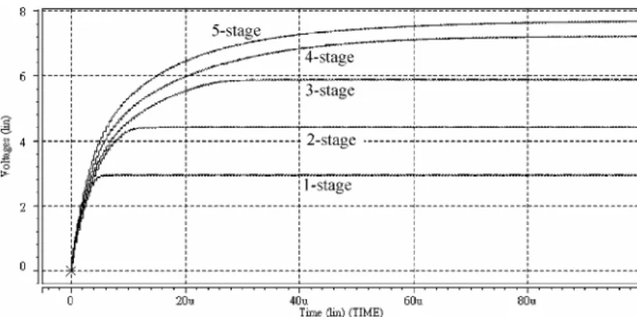
(13) Fig. 2.13. Schematics and cross-section of a charge transfer block. ...................................28. Fig. 2.14. A multi-stage charge pump circuit using the adaptive body connected technique. ...........................................................................................29. Fig. 2.15. The four-phase charge pump circuit. (a) Circuit structure. (b) Clock timing diagram. ...................................................................................31. Fig. 2.16. Operation of the four-phase charge pump circuit. ...............................................32. Fig. 2.17. NCP2 circuit. .......................................................................................................33. Fig. 2.18. Charge pump circuit with extra gate bias circuits. ..............................................34. Fig. 3.1. A three-stage NCP2 using PGI-1 as its output stage. ..........................................40. Fig. 3.2. The graphical solution for obtaining the output saturation voltage in PGI-1 circuit, shown in Fig. 3.1, under NMOS-diode MDC and PMOS-diode MDC where VDD and Vclk are 1.5 V and all the voltages are taken when clk is high. ..................................................................................44. Fig. 3.3. A three-stage PGI-2 circuit. .................................................................................45. Fig. 3.4. A three-stage PGI-3 circuit. .................................................................................47. Fig. 3.5. Vertical structure and internal signals of PMOS CTS MS3 in PGI-3 circuit shown in Fig. 3.4. ..........................................................................48. Fig. 3.6. The output waveforms of PGI-1 circuit under different pump stage with VDD = Vclk = 1.5V, fclk = 2 MHz, and Iout = 10 µA. .....................................49. Fig. 3.7. The output waveforms of various charge pump circuit under different pump stage with VDD = Vclk = 1.5V, fclk = 2 MHz, and Iout = 10 µA. ..................51. Fig. 3.8. Simulated output voltage versus pump stage number of various CPC’s with VDD = Vclk = 1.5V, fclk = 2 MHz, and Iout = 10 µA. .....................................51. Fig. 3.9. Simulated output voltage versus output load current of various 3-stage PGI circuits under different VDD. .........................................................................52. Fig. 3.10. The power efficiency of PGI-1 and PGI-3 circuits versus the output current. ...........53. Fig. 3.11 Microphotograph of the PGI circuits. ..................................................................54 Fig. 3.12. Measured output voltage versus output load current of 3-stage PGI-1 and PGI-3 circuits under different VDD. ...............................................................54. Fig. 3.13. A conceptual block diagram of eight-fold pump gain by using (a) linear growing structure in 7-stage case and (b) exponential-folds structure in 3-stage case. ...................................................55. Fig. 3.14. The block diagram of a 2×2 exponential-gain pump structure. ..........................56. Fig. 3.15. Simulated transient output waveforms of 2×2 CPC and various 3-stage PGI circuits with Vin = Vclk = 1.5 V and Iout = 10 µA. ............................57 xi.
(14) Fig. 3.16. Simulated output voltage versus expected gain of exponential-gain structure, PGI-1, and PGI-3 with Vin = Vclk = 1.5 V and Iout = 10 µA. ...............58. Fig. 3.17. Measured output voltages of 2×2 CPC using PGI-1, PGI-2 and PGI-3 under different supply voltages. ..........................................................................59. Fig. 4.1. Conceptual diagram of an N-stage PGI circuit. ..................................................64. Fig. 4.2. The clock signal, states of switches, and the steady-state waveforms of Vo(m-1), Vo(m), and Vo(m+1). ..................................................................................64. Fig. 4.3. Equivalent model for (a) charging mode of Cm and (b) discharging mode of Cm. ................................................................................66. Fig. 4.4. Equivalent model for the m-th pump stage. ........................................................67. Fig. 4.5. Equivalent model for the first pump stage. .........................................................68. Fig. 4.6. The steady-state waveforms of Vo(N) and Vo. .......................................................69. Fig. 4.7. The supposed steady-state waveforms of Vo(N) and Vo. .......................................71. Fig. 4.8. Equivalent model for the last pump stage and the output stage. .........................74. Fig. 4.9. Equivalent simplified model for the last pump stage and the output stage. ........76. Fig. 4.10 Equivalent model for an N-stage PGI circuit. .....................................................76 Fig. 4.11. Total pump capacitances CTP calculated from the 3-stage model versus the value of K under various desired Vo,avg, where VDD = Vclk = 1.5 V, RL = 100 kΩ, and fs =1 MHz. ................................................80. Fig. 4.12. Total pump capacitances CTP versus the stage number N over various desired Vo,avg, where where K = 1, VDD = Vclk = 1.5 V, RL = 100 kΩ, and fs = 1 MHz. .............................................................................81. Fig. 4.13. Comparison between simulated output waveforms of the equivalent 3-stage circuit and of the corresponding model. ..................................................82. Fig. 4.14. Comparison between simulated output waveforms of the equivalent 3-stage circuit and of the corresponding model under different Cm values. (a) Vo,avg = 5 V and Cm = 150 pF. (b) Vo,avg = 4 V and Cm = 60 pF. (c) Vo,avg = 3 V and Cm = 30 pF. ...........................................................................82. Fig. 4.15. Comparison between simulated output waveforms of the equivalent circuit and of the corresponding model with various numbers of pump stages, where all pump capacitances are fixed at 60 pF. (a) 3-stage for Vo,avg = 4 V. (b) 2-stage for Vo,avg = 3.375 V. (c) 1-stage for Vo,avg = 2.57 V. ..............................................................................83. xii.
(15) Fig. 4.16. (a) Relative errors between the model and the 3-stage circuit for different desired Vo,avg with VDD = Vclk = 1.5 V, RL = 100 kΩ, fs = 1 MHz, and D = 0.5. (b) Corresponding output ripple ∆Vo. .............................................84. Fig. 4.17. (a) Relative errors between the model and the equivalent circuit with different stage number N for Vo,avg = 4 V and D = 0.5. (b) Corresponding output ripple ∆Vo. ..................................................................84. Fig. 4.18. Comparison between simulated output waveforms of the practical 3-stage PGI-3 circuit and of the corresponding model. .......................................85. Fig. 4.19. Comparison between simulated output waveforms of the practical 3-stage PGI-3 circuit and of the corresponding model under different Cm values. (a) Vo,avg = 5 V and Cm = 150 pF. (b) Vo,avg = 4 V and Cm = 60 pF. (c) Vo,avg = 3 V and Cm = 30 pF. ...........................................................................85. Fig. 4.20. Comparison between the simulated output waveforms of the practical 3-stage PGI-3 circuit and of the corresponding model with various numbers of pump stages, where all pump capacitances are fixed at 60 pF. (a) 3-stage for Vo,avg = 4 V. (b) 2-stage for Vo,avg = 3.375 V. (c) 1-stage for Vo,avg = 2.57 V. ..............................................................................85. Fig. 4.21. Measured output voltages of a 2-stage PGI-3 circuit under different values of Cm. ........................................................................................................87. Fig. 4.22. Measured output voltages of a 2-stage PGI-3 circuit with a different ratio of C1 and C2. ................................................................................................88. Fig. 5.1. Conceptual schematic of a conventional charge pump regulator. .......................92. Fig. 5.2. Operation of a regulated charge pump. ...............................................................92. Fig. 5.3. Conceptual schematic of a charge pump regulator using an automatic pumping frequency control scheme. ..............................................93. Fig. 5.4. Conceptual block diagram of a charge pump converter. .....................................94. Fig. 5.5. Two-stage equivalent model. ...............................................................................95. Fig. 5.6. Steady state equivalent circuit. ............................................................................96. Fig. 5.7. Dependence of the output voltage (Vout) on the pump clock frequency (fs) under different resistive loads. .............................................................................97. Fig. 5.8. Dependence of the regulating ability on the central frequency (fc) under different resistive loads, where the mean variance of the output voltage (∆Vf) is resulted from the frequency fluctuation (∆f = 100 kHz) around a specific central frequency. ....................................................................97. xiii.
(16) Fig. 5.9. Magnitude response of the equivalent model, where RL = 50 kΩ, CO = 375 pF, fc = 800 kHz, and the magnitude fluctuation of the input small signal ∆f = 100 kHz. .........................................................................98. Fig. 5.10. Conceptual representation of the basic source coupled multivibrator operation. .....................................................................................100. Fig. 5.11. (a) Schematic of a source coupled multivibrator. (b) Simplified schematic of source coupled multivibrator, where M1 is on and M2 is off. ......................101. Fig. 5.12. Voltage waveforms of the source coupled multivibrator. ..................................101. Fig. 5.13. Overall schematic of the voltage-controlled oscillator circuit. .........................103. Fig. 5.14. Oscillation frequency (fs) versus input control voltage (Vc). .............................103. Fig. 5.15. Output voltage Vout versus input control voltage Vc, where VDD = Vs = 1.5 V, and CO = 375 pF. ...................................................................104. Fig. 5.16. Dependence of the mean variance of the output voltage (∆Vf) on the input operating voltage (Vc), where vc = 50 mV. ....................................105. Fig. 5.17. Bode plot of the modeling charge pump converter, where Vc = 1 V and RL = 50 kΩ. .................................................................................................106. Fig. 5.18. Bode plot of the designed error amplifier with a low supply voltage VDD = 1.5 V. .......................................................................................................108. Fig. 5.19. Charge pump regulator for open-loop test. .......................................................108. Fig. 5.20. Close-loop charge pump regulator without compensation. ............................... 111. Fig. 5.21. Conceptual signal-flow diagram of the close-loop charge pump regulator without compensation. ....................................................................... 111. Fig. 5.22. Magnitude response of the uncompensated regulator: (a) with Vref = 1 V under different resistive load, and (b) with RL = 50 kΩ under different reference voltage. ..................................... 113. Fig. 5.23. Close-loop charge pump regulator with compensation. .................................... 114. Fig. 5.24. Bode plot of the compensated charge pump regulator for RL = 100 kΩ with different reference voltage. ........................................................................ 115. Fig. 5.25. Transient output response of the compensated regulator with a resistive load variation at Vref = 1V. (a) RL is changed from 50 kΩ to 100 kΩ. (b) RL is changed from 50 kΩ to 25 kΩ. ............................................................ 118. Fig. 5.26. Transient output response of the compensated regulator with a reference voltage variation at RL = 50 kΩ. (a) Vref is changed from 1 V to 1.2 V. (b) Vref is changed from 1 V to 0.8 V. ................................................................120. Fig. 5.27. Schematic diagram of a simple compensated charge pump regulator. .............123 xiv.
(17) Fig. 5.28. Transient output response of the practical regulator with a resistive load variation at Vref = 1V. (a) RL is changed from 50 kΩ to 100 kΩ. (b) RL is changed from 50 kΩ to 25 kΩ. ............................................................124. Fig. 5.29. Transient output response of the practical regulator with a reference voltage variation at RL = 50 kΩ. (a) Vref is changed from 1 V to 1.2 V. (b) Vref is changed from 1 V to 0.8 V. ................................................................125. xv.
(18) Chapter 1 Introduction. 1.1 Motivation In recent years, progress has been made towards small, inexpensive, and mobile equipments. The new-generation portables require the use of a single Li-ion cell (i.e. 3.6V normally) or batteries (1.5 V – 3 V) for system power. The growing portable equipment market has created a strong demand for DC/DC converters which can fit the size of the equipment. In addition, in portable mixed-mode systems where the power consumption is critical, the converters that can operate in low supply voltage environments are very desirable and crucial. In view of the device level, dimensions of transistors have been scaled down toward the nanometer region and supply voltages for CMOS integrated circuits have been continuously reduced due to the reliability and power consumption issues. Lower supply voltages result in lower power consumptions so that chip designs migrate to the lower voltage level. Unfortunately, reducing the supply voltage does not offer similar benefits for analog circuits. In order to save the chip area or have the high-speed performance, some circuits are fabricated in advanced low-voltage processes but supplied by higher voltage levels. Besides, some other peripheral components or ICs in an electronic system are still operated in higher voltage environments, such as 3.3 V or 5 V. Thus, a voltage generator circuit, which can operate with a low supply voltage, is demanded to generate a higher voltage than the supply voltage for mixed-voltage operations.. 1.
(19) Charge pump circuit (CPC) is a kind of voltage generators and has been shown to be an effective technology to provide the solution for above demands to convert an input voltage upward to a higher one with either a positive or a reverse polarity on a chip. Since charge pump circuits use capacitors as energy storage devices instead of magnetic components, the converters are amenable to compact and lower cost designs without electromagnetic interference (EMI) problems. For low power designs, the capacitors needed by charge pump circuits could be small enough to be fabricated in integrated circuits. Thus, charge pump circuits are suitable for portable systems with only one battery as its power supply and for low-voltage chip design. With the continued shrinking of handheld devices such as cell phones, PDAs, pagers and laptops, the use of charge pump converters is becoming more attractive over inductive based structures.. 1.2 Applications of Integrated Charge Pump Circuits Generally, integrated charge pump circuits are used to provide output voltages higher than the power supply. They have been extensively applied in nonvolatile memories for many years, such as Electrically Erasable Programmable Read Only Memory (EEPROM) and flash memory that require a high voltage to program the floating-gate devices for rewriting data [1]-[14]. Recent development of low voltage circuit design, charge pump circuits can also be adopted to power ICs and analog switch circuits, such as switched-capacitor filters and A/D converters, for generating high voltages to control MOS gates at high or low level in order to perform “ON” or “OFF” operations [15]-[16].. 1.2.1 EEPROM and Flash Memory For electrical re-programmability in floating-gate devices, EEPROMs and flash memories. 2.
(20) depend on a technology mechanism referred to “Fowler-Nordheim (F-N) tunneling” or “cold electron tunneling”. The effect of tunneling allows electrons to pass through the energy barrier at the silicon-silicon dioxide (Si-SiO2) interface at a lower energy than the 3.2 eV required passing over this energy barrier. Based on the F-N tunneling mechanism, the floating gate tunneling oxide cell was developed by Intel and has been one of the most common EEPROM cell [8]-[9]. As shown in Fig. 1.1, a basic cell of an EEPROM contains a select transistor and a double polysilicon storage transistor with a floating polysilicon gate isolated in silicon dioxide capacitively coupled to a second polysilicon control gate which is stacked above it. A thin dielectric layer between the floating gate and the source enables the flow of electrons into and from the floating gate during program/erase operations, by means of F-N tunneling.. (a). Fig. 1.1. (b) (a) Circuit symbol and (b) cross section of a basic EEPROM cell [8].. 3.
(21) In the program mode, a positive high voltage is applied to the control gate of the cell, while the drain is floating and both the source and the substrate are grounded. The floating gate is charged negatively with electrons tunneling from the source through the thin oxide. The stored negative charge on the floating gate shifts the threshold voltage of the transistor toward the positive value. In a subsequent program operation, the transistor will not conduct channel current so that the transistor will be “off”. Fig. 1.2(a) shows the floating gate transistor during programming. The erase operation removes electrons from the floating gate by applying a positive high voltage at the source, while the drain is floating and both the control gate and the substrate are grounded. As shown in Fig. 1.2(b), electrons tunnel from the floating gate to the source leaving the floating gate relatively more positively charged. Thus, the threshold voltage is shifted in the negative direction. During subsequent erase operation, the channel current would flow so that the transistor will be “on”. Fig. 1.3 shows the shift in the iD –vGS characteristic of a floating-gate transistor as a result of programming or erasing. To read the content of the memory cell, a suitable voltage vGS, employed mainly by the supply voltage, somewhere between the low and high threshold voltages (VT0 and VT1) can be applied.. (a). (b) Fig. 1.2 (a) Program configuration and (b) erase configuration of a double polysilicon storage transistor in a basic EEPROM cell [10].. 4.
(22) Fig. 1.3: Illustrating the shift in the iD –vGS characteristic of a floating-gate transistor as a result of programming or erasing [11].. In the conventional scheme, F-N tunneling erase has been achieved by raising the source junction to a positive high voltage and grounding the control gate. The source junction is formed to be a double diffusion structure in order to obtain a high breakdown voltage. The deeply formed drain junction prevents channel length scaling, which is required for high-density memory cells. The negative-gate-biased source erase scheme can overcome this problem by applying a negative voltage to the control gate to obtain F-N tunneling. The source voltage necessary for F-N tunneling can be reduced to the supply voltage VDD. Fig. 1.4 shows a conventional double diffusion structure compared with the negative-gate-biased source erase scheme, which has the benefit of scaling down the channel length.. Fig. 1.4. Negative-gate-biased source erase scheme [1].. 5.
(23) Due to the two-transistor type cell, byte-write and byte-erase abilities are accomplished by the EEPROM. However, a major disadvantage of the EEPROM is in a large size of the two-transistor memory cell and that has kept the cost high. Flash memory is a direct derivate of the one-transistor cell EPROM (Erasable Programmable Read Only Memory). It resulted from innovative cell designs and improved technology that allowed the one-transistor cell EPROM to be reprogrammed electrically in the system. Many of the flash memory cells that have developed use the split gate concept in which the separate select and storage transistor gates of the EEPROM are merged into a single device with the channel region shared by the two gates [10]-[12]. Thus, the flash memory has a smaller chip size and a higher density compared to EEPROM. However, unlike EEPROMs with byte-write and byte erase abilities, the flash memory only can be programmed or erased by section. No matter which nonvolatile memory scheme is used, a high voltage with either a positive or a reverse polarity to obtain F-N tunneling is critical in a floating gate structure. As these voltages can be provided externally or generated within the device, memory chips can be divided into double-supply and single-supply devices. In the former case, one supply pin (VDD) is used for the general-purpose supply, and the other pin (VPP) is devoted to program/erase operations (obviously, VPP is higher than VDD). In the latter case, only the VDD pin is present, and all other voltages are generated on-chip. The charge pump circuit is a common on-chip voltage generation for producing any voltage between ground and the power supply on a memory chip [13]-[14]. Furthermore, it is also possible to generate high voltages that are below ground and above the power supply value for creating F-N tunneling. A block diagram of a common flash EEPROM is shown in Fig. 1.5. In this figure, charge pump circuits not only generate large positive and negative voltages (VH) of up to 20 V for programming and erasing but also provide medium voltage (VP) of around 5 V to control the operation mode. Since VH and VP are generally applied to the control gate and the source junction, respectively, the drivability of the VH generator can be set lower 6.
(24) than the VP one. In addition, a reference voltage is needed to control VH and VP to achieve the required stable value which must be guaranteed for accurate read/write/erase operation of the memory cell.. Fig. 1.5. Block diagram of a common flash EEPROM [14].. 1.2.2 Switch Capacitor System Switched-capacitor (SC) technique is an efficient way of implementing analog functions in CMOS technology due to its intrinsic resolution and accuracy. The elements required for the realization of SC circuits are capacitors, switches, and op amplifiers. However, the supply voltage reduction of modern ICs due to technology scaling has a drastic impact on switched-capacitor circuit performance. This is not only due to dynamic range reduction but also because, below a certain supply voltage, switches cannot be driven by adequate overdrive, and their switch-on condition cannot be easily guaranteed over acceptable signal ranges [17]. Thus, conventional CMOS transmission gates may no longer be adequate or even functional as analog switches if the signal swing of the switch control is kept between the nominal supply voltages.. 7.
(25) Recently, switched-capacitor circuits at very low supply voltages could only be realized either in a special process with extra low threshold voltage (VT) of transistors or by using an on-chip voltage multiplier, which generates higher switch control voltages to drive critical switches. The voltage multiplier needed for SC designs is often derived from the EEPROM technology by means of using charge pump circuits and the structure of high voltage generator. For example, as shown in Fig. 1.6, a common high voltage generator consists of five circuit blocks: the charge pump circuit (CPC), the low-pass filter (LPF), the high voltage sensor (HVS), the voltage-controlled oscillator (VCO), and the non-overlapped clock buffer (NOCB). A negative feedback loop is formed to stabilize the output voltage Vout,H and the pump ability is adjusted by the frequency of non-overlapped clocks. The voltage sensor can detect Vout,H and transfer it to a voltage Vc for controlling the voltage-controlled oscillator. If Vout,H is less than the desired value, the voltage Vc generated by HVS is fed to VCO for increasing the frequency of non-overlapped clocks through NOCB. Thus, Vout,H will be pumped to the desired value. Otherwise, the clock frequency is decreased for pushing down Vout,H to the desired lower value [18]-[21].. Fig. 1.6. Architecture of a common high voltage generator.. 8.
(26) Fig. 1.7 illustrates the example of a low-voltage switched capacitor system. The signal paths are fully differential to maximize noise immunity against disturbances from supplies and substrate when digital circuits and switch circuits are on the same chip. The analog signal paths operate directly between the two main power supply lines VDD and VSS. To maximize SNR, a signal swing extending near the supply voltages is necessary. The analog switches are implemented with NMOS transistors so that an on-chip high-voltage generator is used to generate the high-voltage VHH required to completely turn on the NMOS switches.. Fig. 1.7. An example for low-voltage switched-capacitor system [18].. 1.3 Contributions of the Dissertation A charge pump styled voltage generator utilizing the exponential-folds structure and the pumping gain increase (PGI) circuits with high voltage transfer efficiency is proposed. PGI circuits used in the linear DC/DC converter are proposed to solve the threshold voltage problem and the limitation of the diode-configured output stage so that the boosted output voltage increases more linearly versus the pumping stage number. With the exponential-folds structure, fewer voltage pump stages are needed to obtain the higher output voltage and. 9.
(27) further improve the voltage pumping gain. Especially, this design still has good efficiency with a low input supply voltage such as one battery cell. In addition, a complete equivalent model of high efficiency PGI circuits with a resistive load and the corresponding thorough analysis are proposed. Based on this analytical model, characteristics of PGI circuits can be approximately predicted and several handy equations, which are useful for a pencil-and-paper design, can also be found for planning the desired circuit to achieve good enough performance with an acceptable accuracy tolerance in the steady state. In addition, an optimized design method for PGI circuits with a resistive load is developed in terms of the total number of gain stages in the design and the ratio between pump capacitors. Furthermore, since the proposed model provides a good substitute for a practical PGI circuit for mathematical analysis. By using this equivalent model, a feedback control scheme of the charge pump regulator can be easily planned for adjusting operation to obtain a desired output voltage under different conditions. A design procedure of a charge pump regulator is presented by an example to describe and demonstrate the feasibility. Briefly, the thesis illustrates several solutions of charge pump designs, so that charge pump styled voltage generators for varied low-voltage applications with good enough performance can be obtained easily.. 10.
(28) 1.4 Organization The thesis is organized into six chapters. Chapter 1 is the introduction and indicates the most popular application about charge pump styled voltage generators. Chapter 2 introduces previous studies and explains their features and limitations. The survey focus on some typical circuit topologies in charge pumps. Chapter 3 presents the pumping gain increase circuits dealing with the augmented threshold voltage problem in the pump stages and depicts a new idea of exponential-folds structure to obtain a higher output voltage with fewer voltage pump stages. Chapter 4 illustrates an equivalent model of PGI circuits for a pencil-and-paper design. Characteristics of PGI circuits can be designed effectively through this model to achieve good enough performance with an acceptable accuracy tolerance in the steady state. Chapter 5 depicts a design procedure with consideration of the equivalent model to plan a charge pump regulator. A design example is used to describe and demonstrate the feasibility. Chapter 6 summarizes the main results of this dissertation. Then, some suggestions for future works are also addressed in this chapter.. 11.
(29) Chapter 2 A Survey of Previous Charge Pump Circuits. 2.1 Introduction In modern mixed-mode circuit designs, low-voltage and small-size voltage generators have been extensively required. Charge pump circuits (CPCs) can provide an effective technology required to meet these demands to convert the voltage upward to a higher one with either a positive or a reverse polarity. Since CPCs use capacitors as energy storage devices instead of magnetic components, the voltage generators have no electromagnetic interference (EMI) problems and are amenable to compact and lower cost designs. For low power designs, the capacitors required by CPCs can be small enough to be fabricated in integrated circuits. Most charge pumps are based on the circuit proposed by Dickson that uses diode-connected MOSFETs as charge transfer devices [22]-[25]. In this design, the maximum output voltage is limited by the threshold voltage Vt loss problem of the diode-connected MOSFETs due to the body effect. When more pump stages are employed for producing higher pumping voltages, the body effect will be getting more serious. Therefore, the voltage pumping gain will be further reduced and the pumping efficiency will be highly degraded. In recent years, several modifications of the Dickson CPC have been proposed to alleviate the augmented threshold voltage problem. It is possible to use process topology to reduce the body effect problems [1], [26]-[29]. Without making alterations in process, several attempts 12.
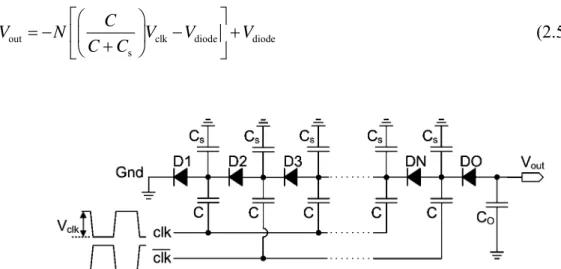
(30) have been made to alleviate the Vt loss problem by circuit topologies. The four-phase pulse CPC is the favorable style in the electronics market [1], [30], [31]. However, this circuit uses a more complicated timing control scheme. Some designs use isolated body techniques [6], [32], but these techniques require extra cost due to utilization of triple-well technology that increases the layout and process complexity. Additional gate biasing circuits used to dynamically control the transfer devices are also popular in charge pump designs [33], [34]. Nevertheless, the pumping gain is still degraded by the Vt loss problem in some of these circuits [33]-[36]. In addition, another voltage drop problem also exists at the output stage and degrades the total pumping efficiency further. In this chapter, some typical topologies based on Dicksons CPC will be introduced and discussed.. 2.2 Dickson Charge Pump Circuit 2.2.1 Dickson CPC The N-stage positive Dickson CPC using pn-junction diodes as the charge transfer devices is shown in Fig. 2.1 [22]. The voltage at each node is pumped by the charge transferred along the diode chain as the coupling capacitors are successively charged and discharged during each half of the clock cycle. Since voltages in the diode chain are not reset after each pump cycle, the average potentials of all nodes increase progressively from the input to the output.. Fig. 2.1 An N-stage positive Dickson charge pumps implemented by pump capacitors in parallel with diode chain [22].. 13.
(31) In this structure, C and Cs are pump capacitors and stray capacitors, respectively, and Dn is the pn-junction diode in the n-th stage. The supply voltage is VDD and the circuit is driven by two anti-phase clock signals clk and clk with amplitude Vclk which is usually equal to VDD. When clk is high and clk is low, the diodes of even stages are forward bias and transfer charges to the succeeding pump capacitors. Similarly, when clk is low and clk is high, the diodes of odd stages are forward bias and transfer charges to the succeeding pump capacitors. After several cycles of pump operations, the output voltage of this charge pump circuit shown in Fig. 2.1 can be pumped high by charges pushed from the power supply to the output node stage by stage. Using the steady-state analysis from the simple model of the Dickson charge pump [22] – [24], the voltage fluctuation ∆Vn,diode in the n-th stage associated with the voltage division resulting from a clock coupling capacitance C and a stray capacitance Cs can be expressed as ⎛ C ⎞ I out ∆Vn ,diode = ⎜ − Vdiode ⎟ Vclk − f ( C + Cs ) ⎝ C + Cs ⎠. (2.1). where f is the clock frequency, Iout is the output current, and Vdiode is the turn-on voltage of the pn-junction diode (the forward bias diode voltage or the diode cutoff voltage). In (2.1), the first term is the common expression of the voltage swing occurring at each pump node contributed by the clock source, clk or clk , through the associated pump capacitor C. The second term is shown the voltage drop due to Iout. If Cs and Iout are small enough and C is large enough, Cs and Iout can be ignored from (2.1). Since Vclk is usually the same as the normal power supply voltage VDD, the voltage fluctuation of each pump node can be simply expressed as. ∆Vn ,diode ≈ Vclk − Vdiode = VDD − Vdiode. (2.2). Thus, ∆Vn,diode can be regarded as the pumping gain of the n-th stage. In each stage, the necessary condition for the boost function of the charge pump circuit is that ∆Vn,diode must be. 14.
(32) larger than zero. With the condition that Vdiode and ∆Vn,diode are constants, the total pumping voltage in an N-stage Dickson charge pump circuit with a load can be obtained as. ⎡⎛ C ⎞ ⎤ I out Vout − VDD = N ( ∆Vn ,diode ) − Vdiode,DO = N ⎢⎜ − Vdiode ⎥ − Vdiode,DO ⎟ Vclk − f ( C + Cs ) ⎣⎝ C + Cs ⎠ ⎦ (2.3) Hence, the output voltage of the N-stage diode charge pump circuit can be expressed as. ⎡⎛ C ⎞ ⎤ I out Vout = VDD − Vdiode,DO + N ⎢⎜ − Vdiode ⎥ . ⎟ Vclk − f ( C + Cs ) ⎣⎝ C + Cs ⎠ ⎦. (2.4). where Vout is the output voltage, VDD is the input supply voltage, Vclk is the voltage amplitude of the pump clock signals, Vdiode is the voltage drop of a forward bias diode, N is the total stage number, Iout is the output current loading, and f is the frequency of the driving clock signals. Through the similar structure, Fig. 2.2 shows the N-stage negative Dickson charge pump circuit using pn-junction diodes as the charge transfer devices. As the above description, the output voltage of the N-stage charge pump circuit without output loading current can be expressed as. ⎡⎛ C ⎞ ⎤ Vout = − N ⎢⎜ ⎟ Vclk − Vdiode ⎥ + Vdiode ⎣⎝ C + Cs ⎠ ⎦. (2.5). Fig. 2.2 An N-stage negative Dickson charge pumps implemented by pump capacitors in parallel with diode chain.. 15.
(33) However, it is difficult to implement isolated diodes in the common silicon substrate. In the past, some nonvolatile memory products were developed in a p-well process in which the whole substrate could be brought to the high programming voltage such that the drain-top-well junction of the NMOS transistor can be used as diode. However, this is unacceptable if the high voltage is generated on chip [24]. In other words, the charge pump circuit with diodes shown in Fig. 2.1 and Fig. 2.2 can not be easily fabricated into the standard CMOS process. Therefore, in the MOSFET technology, diode-connected transistors are being substituted for the diode chain and are used to transfer the charge in one direction. Fig. 2.3 shows the N-stage Dickson charge pump circuit implemented by pump capacitors in parallel with diode-connected MOSFETs.. Fig. 2.3 An N-stage Dickson charge pumps implemented by pump capacitors in parallel with diode-connected MOSFETs.. When the diode-connected MOSFET is forward bias, the drain-source voltage drop (Vds) across the NMOS-diode is identical to its threshold voltage Vtn. Neglecting the body effect, the voltage fluctuation ∆Vn of the n-th pump stage and the output voltage of the N-stage Dickson charge pump circuit have been derived as ⎛ C ⎞ I out ∆Vn = ⎜ − Vtn,MDn ⎟ Vclk − f ( C + Cs ) ⎝ C + Cs ⎠. (2.6). and. 16.
(34) ⎡⎛ C ⎞ ⎤ I out Vout = VDD − Vtn,MDO + N ⎢⎜ − Vtn,MDn ⎥ ⎟ Vclk − f ( C + Cs ) ⎣⎝ C + Cs ⎠ ⎦. (2.7). where Vtn,MDn denotes the threshold voltage of the n-th diode-connected MOSFET MDn.. 2.2.2 Equivalent Model of the Dickson CPC From (2.7), an extremely simple equivalent circuit for the Dickson charge pump is shown in Fig. 2.4 and the output voltage can be derived as. Vout = Veq − Req I out. (2.8). where. ⎡⎛ C ⎞ ⎤ Veq = VDD − Vtn,MDO + N ⎢⎜ ⎟ Vclk − Vtn,MDn ⎥ ⎣⎝ C + Cs ⎠ ⎦ Req =. N f ( C + Cs ). (2.9). (2.10). In (2.8), Veq and Req are the equivalent open-circuit output voltage and the equivalent output series resistance, respectively [23]-[25]. There will be a voltage ripple at the output due to the discharging of the output capacitance CO by the resistive load RL.. Fig. 2.4. Equivalent model of the Dickson charge pump.. In deriving this model for the voltage multiplier, it has been assumed that all of the pump capacitors are completely charged and discharged with the same drain-source voltage drop across each diode-connected MOSFET. Thus, the output voltage keeps increasing with increasing stage number and theoretically any pump voltage can be generated. 17.
(35) In practice this is not the case due to the undesirable characteristic of the diode-connected MOSFET, such as internal series resistance and the body effect. Since the model is based on the approximation of the uniform threshold voltage, the error introduced by this approximation will of course be generated. This results in unequal voltage drops across each pump stage and a nonlinear manner with load current [23]-[25].. 2.2.3 Limitation of the Dickson CPC In a standard CMOS process, all NMOS transistors have a common body at p-substrate so that the body potentials Vb will be equalized. Thus, the problem of body effect cannot be disregard in charge pump circuits based on diode-connected MOSFETs. In Fig. 2.3, since the substrate terminal is grounded, the common body potential Vb is equal to zero. Thus, different source-substrate voltages (Vsb) are applied to diode-connected MOSFETs and cause different threshold voltages on NMOS transistors. The dependence of the threshold voltage on the source-substrate voltage is expressed as. Vt = VT0 + γ ⋅ ⎡⎣ Vbs + 2φ f − 2φ f ⎤⎦. (2.11). where VT0 is the threshold voltage for Vbs = 0 V, φ f is the band bending in the substrate needed to invert the silicon surface, and γ denotes the body effect coefficient. In (2.11), it can be seen that as the node voltage of each stage increases by the charge pump, the increased reverse-biased source-substrate junction voltage will increase the threshold voltage of the NMOS transistor due to the body effect. Thus, from (2.6) to (2.10), the voltage fluctuation ∆Vn of each pump stage is not a constant because Vtn,MDn is enlarged by the body effect, which increases as more pump stages are used. The increased threshold voltage Vtn results in the degradation of ∆Vn and that can be given as ∆V1 > ∆V2 > """ > ∆VN −1 > ∆VN. (2.12). where. 18.
(36) Vtn,MD1 < Vtn,MD2 < """ < Vtn,MDN < Vtn,MDO. (2.13). The maximum voltage drop occurs in the output stage, referred to Vtn,MDO, because the most serious body effect occurs on MDO due to a large build up of Vsb. Thus, the pumping efficiency of the succeeding stage will be less than that of the forestages. When more pumping stages are used, the Vt augmentation problem will be more serious and will result in the degradation of the output voltage [6], [32]-[36]. It can be obvious that if more cascaded pump stages are added in, Vtn,MDN in the last pump stage and Vtn,MDO in the output stage will increase. Once ∆VN in the last stage reduces to zero, Vout will start to saturate. In other words, if the total pump stage number N is increased further, the pumping efficiency of the Dickson charge pump circuit is degraded and the maximum output voltage is limited. Thus, the output voltage cannot be maintained as a linear function of the number of stages and the pumping efficiency will be highly degraded as the number of stages increases further. In the low-voltage system where VDD and Vclk are small, since the threshold voltage cannot be scaled down as the scaling trend of the supply voltage, the Vt augmentation problem makes a great impact on the final pump voltage and the pumping gain will be further reduced [6], [31]-[33]. The loss of pumping gain also results in an increased power loss [35]. This low efficiency restricts the application of the Dickson charge pump structure to low supply voltage systems.. 2.3 Improved Charge Pump Circuits based on Process Topology Several modified charge pump circuits based on the Dickson structure were reported to enhance the pumping efficiency [1], [6], [23]-[36]. Based on process techniques, several attempts have been made to implement fully isolated p-n junction diodes in the Dickson charge pump circuit shown in Fig. 2.1 [1], [26]-[29]. Besides, in the case of using MOS-. 19.
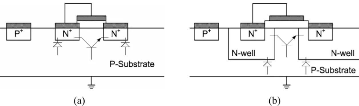
(37) diodes as transfer devices, some processes make use of ion implantations to adjust the threshold voltage of the transistor to the desired value and to improve the punch-through feature of transistors.. 2.3.1 Normal Transfer Device Traditionally, a p+/n-well diode with the grounded p-substrate as shown in Fig. 2.5 is a kind of p-n junction diodes in the standard CMOS process; nevertheless, an undesired parasitic p-n junction exists between the n-well and the grounded p-type substrate. If the voltage on the cathode of the p+/n-well diode is larger than the junction breakdown voltage between the n-well and the grounded p-substrate, the charge on the cathode will leak to ground through this parasitic p-n junction. Besides, it can also be found that the p+/n-well diode exhibits a vertical parasitic bipolar transistor, which is in part responsible for leakage currents.. Fig. 2.5 Cross-section of an p+/n-well diode created on an n-well using p+ and n+ diffusions with the grounded p-substrate.. A diode-connected NMOS transistor, whose gate and drain are connected, with the grounded p-substrate is another kind of p-n junction diodes in the standard CMOS process as shown in Fig. 2.6(a). Similarly, an undesired p-n junction parasitizes between the n+ region (source/drain) and the grounded p-type substrate. If the voltage on the cathode or anode of the transistor is larger than the junction breakdown voltage between the n+ region and the grounded p-type substrate, the charge will also leak to ground through this parasitic junction.. 20.
(38) It is also found in this structure that the lateral parasitic bipolar transistor would result in leakage currents.. (a) (b) Fig. 2.6 Cross-section of an diode-connected NMOS transistor with the grounded p-substrate. (a) Standard NMOS transistor. (b) High voltage NMOS transistor.. Another high breakdown voltage structure of an NMOS transistor is that the source and drain regions are surrounded by separate n-wells shown in Fig. 2.6(b). The n-well is lower doped than conventional n-diffusions thus allowing the possibility of a higher breakdown voltage. Using this power NMOS to substitute for a standard NMOS in diode-connected style, it can be seen that higher breakdown voltages of the power NMOS will reduce the limitation from undesired junctions. However, the layout is atypical in that the active layer was added beneath the gate in order to achieve thin oxide in the gate to n-well overlap region. Consequently, while above normal transfer devices are used in the Dickson charge pump circuit, the maximum output voltage and the pumping efficiency will be limited by the breakdown voltage of the undesired junction. In addition, parasitic devices are in part responsible for leakage currents.. 2.3.2 Utilizing Body Diode as the Transfer Device The implementation of silicon-on-insulator (SOI) MOSFET body diodes in place of typical transfer devices reduces the voltage drop across each stage and increases the voltage efficiency of the charge pump [27]. In an SOI process, each MOSFET body is isolated from 21.
(39) neighboring transistors due to the buried oxide (BOX) layer. The cross section of an n-channel SOI transistor is shown in Fig. 2.7, and the two p-n junctions of this structure form a back-to-back diode configuration as indicated in the drawing.. Fig. 2.7. Cross-section of an SOI n-channel device for body diode connection.. For body diode implementation, the floating-body of the n-channel is connected to the drain, thus shorting the junction from the p-type body to the n-type drain. Hence, only one diode exists between the gate-drain-body connection and the source. In this configuration, the gate-drain-body connection will serve as the anode and the source as the cathode. Fig. 2.8 shows the two-dimensional structure of an SOI NMOS body-diode under gate-drain-body connection. The vertical white line represents the p-n junction of the body diode, where the right side is the anode or p-type region of the NMOS structure and the left side is the cathode or n-type source region. The build-in voltage across this silicon body diode is approximately 0.4 V. Comparing with the transfer device realized by transistors in the diode-connected style, using body diodes can prevent the augmented threshold voltage problem as the pump stage number increases. Furthermore, since the device is isolated to others by the insulation layer in the SOI CMOS process, charge pump circuits realized by the body diode can pump the output voltage higher without the limitation of parasitic p-n junctions, such as the breakdown voltage of undesired 22.
(40) junctions or leakage currents. However, the voltage pumping gain per stage is still reduced by the build-in voltage of the body diode, and the SOI CMOS process is more expensive than the common bulk CMOS process.. Fig. 2.8 2-D structure of an SOI NMOS body-diode [27].. 2.3.3 Utilizing Polysilicon Diode as the Transfer Device In the past, it is difficult to implement fully isolated p-n-junction diodes in the common silicon substrate. In the recent sub-quarter-micron standard CMOS process with shallow trench isolation (STI) [37], the polysilicon diode, which is fully isolated from the silicon substrate, can be implemented and applied in the charge pump circuit [28]. As shown in Fig. 2.9, the polysilicon diode can be realized on the polysilicon layer in the recent STI process which has separated doping impurities for PMOS and NMOS gates. The STI layer is located above the silicon substrate. The intrinsic polysilicon layer is deposited on the STI layer, and then the p-type and n-type impurities are doped into the intrinsic polysilicon layer to form the PMOS gate and the NMOS gate, respectively. An extra un-doped (intrinsic) polysilicon region (i) can be inserted between the p-type and n-type doped polysilicon regions. The length Lc of the un-doped region can be used to adjust the I–V. 23.
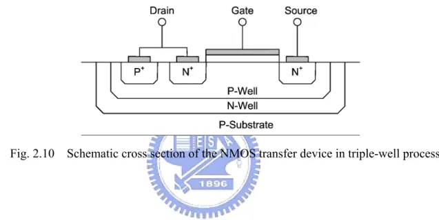
(41) characteristic of the polysilicon diode.. Fig. 2.9. Schematic cross section of the polysilicon diode.. Because the polysilicon diode is implemented on the STI layer, it is isolated from the silicon substrate. Charges on the anode and the cathode of the polysilicon diode would not leak to the silicon substrate. In addition, the parasitic capacitance of the polysilicon diode formed on the STI layer has been studied in [38], which is smaller than those of traditional p+/n-well junction diodes and MOS diodes. Therefore, the polysilicon diode can be applied to the charge pump circuit without the limitation of parasitic junctions for achieving better pumping efficiency.. 2.3.4 Utilizing Triple-Well Technique Triple-well technology has become popular for charge pump circuit fabrication as it allows easier handling of the negative voltages necessary when the negative-gate erase technology is adopted. With this kind of technology shown in Fig. 2.10, p-well/n+ junction diodes can be used with no risk of charge injection into the substrate, since the p-well region is isolated from the p-substrate by a reverse-biased n-well. In addition, when the triple-well process is used, the gate-drain connection for a MOS diode, which implements a charge transfer device, can also be applied with isolation. Therefore, based on the triple-well technology, p-well/n+. 24.
(42) junction diodes or MOS diodes applied to the charge pump circuit would reduce the leakage current from parasitic junctions. However, if the triple-well p-well/n+ junction diode is used, the pumping voltage per stage is still reduced by the build-in voltage. If the triple-well MOS diode is applied, the Vt augmentation problem still exists and the pumping efficiency of the succeeding stage is still less than that of the forestage.. Fig. 2.10. Schematic cross section of the NMOS transfer device in triple-well process.. 2.4 Improved Charge Pump Circuits based on Circuit Topology Besides process topologies, several modifications based on circuit topologies were used to enhance the pumping efficiency [6], [29]-[34]. Normally, these circuit topologies employ additional control circuits or multiple timing control scheme of pump clocks to reduce the Vt loss problem without making alterations in process.. 2.4.1 Floating-Well Technique Fig. 2.11 shows the floating-well technique using PMOS diodes as charge transfer devices [6]. The floating-well technique can be utilized to eliminate the body effect issue on diodeconnected PMOS transistors in the Dickson charge pump circuit.. 25.
(43) Fig. 2.11. Floating-well charge pump circuit using PMOS diodes as charge transfer devices.. For proper operations with floating-well condition, PMOS transistors are used with their body (n-well) floating as shown in Fig. 2.12(a), and Fig. 2.12(b) shows the internal signals. During the first phase (clk is high and clk is low), Vn is high and the transistor Mn is off. Meanwhile, Vn+1 is at its low level and the transistor Mn+1 is turned on for transferring charges from Cn to Cn+1. The n-well potential of Mn+1 denoted to Vw,n+l is initially set to. VW, n +1 = Vn − Vbuilt -in. (2.14). where Vbuilt-in is the built-in potential of p+ to n-well diode and Vn can be considered as the source voltage of Mn+1. From (2.14), Vsb of Mn+1 is given as. Vsb = Vn – Vw,n+l = Vbuilt-in. (2.15). Thus, the threshold voltage could be fixed due to a constant Vsb in the conducting PMOS diode. In addition, at the beginning of charge transfer, Vsb of Mn+1 is equal to Vbuilt-in (> 0 V), which means the effective threshold voltage (Vtp) of the PMOS transistor is even slightly lower than the body-effect free threshold voltage (VTP0). Thus, the Vt augmentation problem can be reduced, and the output voltage would be higher than that of the conventional Dickson CPC. Furthermore, the same floating-well concept also can be utilized for NMOS transistors, but it requires the triple-well process to fabricate NMOS diodes in a separated pocket p-well.. 26.
(44) (a). Fig. 2.12. (b) (a) Vertical structure and (b) internal signals of the floating-well charge pumps.. Utilizing floating-well technique in charge pump circuits exhibits the output characteristic similar to that of a charge pump circuit with an ideal diode chain. The pumping efficiency would be increased rather than the traditional CPC with MOS diode configuration limited by the Vt augmentation problem. In addition, the floating-well charge pump circuit can generate enough voltages even at a supply voltage less than 2.0 V. However, the voltage pumping gain per stage is still reduced by the threshold voltage.. 27.
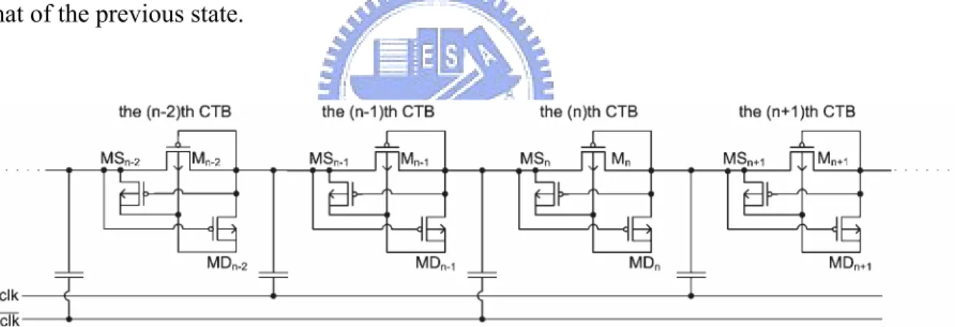
(45) 2.4.2 Adaptive Body Technique The adaptive body technique mitigates the limitation of the varying threshold voltage encountered in the basic Dickson design. The main idea is to control the body of the MOSFET as an active terminal to avoid the problem associated with the threshold voltage increase in charge transfer MOSFETs [32]. By adjusting the body voltage, Vsb and Vth of the transistor used as a switch in each pump stage are kept constant. With no threshold voltage increase, a higher output voltage can be obtained. Fig. 2.13 shows the charge transfer block (CTB) with two auxiliary MOSFETs to dynamically bias the body terminal of the diode-connected MOSFET through the schematic and the cross-section view. For each charge transfer block, two auxiliary MOSFETs and one charge transfer MOSFET share the body separated from the body of other blocks.. Fig. 2.13. Schematics and cross-section of a charge transfer block.. 28.
(46) A multi-stage charge pump circuit using the adaptive body connected technique is shown in Fig. 2.14. The body voltage of the n-th charge-transfer MOSFET Mn is set by the source-side auxiliary transistor MSn and the drain-side auxiliary transistor MDn in the n-th charge transfer block. When clk is low and clk is high, Mn is ON and MSn turns on. Then, the source and the body of Mn are connected through MSn, so that the body potential is approximately equal to the potential of the source of Mn. In this way, since no reverse bias exists between the source and the body of the charge-transfer MOSFET, the threshold voltage of Mn stays with. VTP0 (threshold voltage for Vsb = 0 V) during the charge transfer state preventing the Vt augmentation problem. In the same clock state, Mn-1 is OFF and MDn-1 turns on so that the drain and the body of the (n-1)th charge transfer MOSFET are connected to prevent the body from floating. When clk is high and clk is low, the pump operates in opposite manners as that of the previous state.. Fig. 2.14. A multi-stage charge pump circuit using the adaptive body connected technique.. Based on this technique, the body voltage of the charge-transfer MOSFET keeps track of higher value of the source or the drain voltage at each clock state by auxiliary MOSFETs. Since the source-body voltage in each CTB stage no longer increases, the threshold voltage will remain relatively constant throughout the chain. Therefore, the problem of increasing threshold voltages can be minimized, and the charge pump equation becomes identical to that of an ideal-diode Dickson CPC as (2.4). However, this adaptive body connected technique increases the parasitic capacitance at 29.
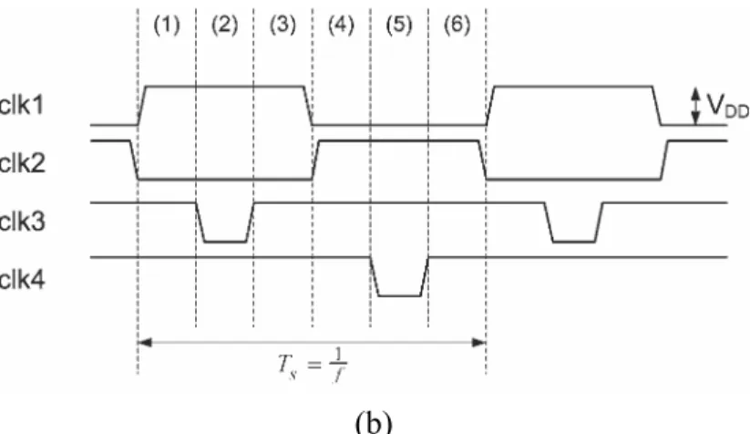
(47) each pumping node due to a large bulk-to-well pn-junction capacitance, so pump capacitances have to be enlarged. The auxiliary MOSFETs used to dynamically control the body terminal of the diode-connected MOSFET may also generate the substrate current in the floating-well device.. 2.4.3 Four-Phase Technique The four-phase charge pump circuit is the favorable style in the electronics market. Using special four-phase clocks, the gain degradation due to threshold voltage can be alleviated [1], [30], [31], [39]. Fig. 2.15 shows the schematic and the clock timing diagram of an example of the four-phase charge pump circuit. C1 and C2 are pump capacitors, and M1 and M2 are charge transfer transistors with their gates driven by clocks through Cs1 and Cs2. Ms1 and Ms2 are transistors used to precharge the gates of M1 and M2, respectively. Instead of NMOS transistors in the conventional charge pump circuit, PMOS transistors are adopted for all of charge transfer transistors and precharging transistors. In addition, a individual n-well of PMOS transistor is employed in each unit stage for isolation.. (a). 30.
數據

+7
相關文件
• helps teachers collect learning evidence to provide timely feedback & refine teaching strategies.. AaL • engages students in reflecting on & monitoring their progress
Robinson Crusoe is an Englishman from the 1) t_______ of York in the seventeenth century, the youngest son of a merchant of German origin. This trip is financially successful,
fostering independent application of reading strategies Strategy 7: Provide opportunities for students to track, reflect on, and share their learning progress (destination). •
Strategy 3: Offer descriptive feedback during the learning process (enabling strategy). Where the
How does drama help to develop English language skills.. In Forms 2-6, students develop their self-expression by participating in a wide range of activities
Now, nearly all of the current flows through wire S since it has a much lower resistance than the light bulb. The light bulb does not glow because the current flowing through it
The existence of cosmic-ray particles having such a great energy is of importance to astrophys- ics because such particles (believed to be atomic nuclei) have very great
This kind of algorithm has also been a powerful tool for solving many other optimization problems, including symmetric cone complementarity problems [15, 16, 20–22], symmetric
