CMOS process. By reducing the voltage difference across the gate oxide of the devices in the ESD detection circuit, the proposed power-rail ESD clamp circuit can achieve an ultralow standby leakage current. In addition, the ESD-transient detection circuit can be totally embedded in the SCR device by modifying the layout structure. From the measured results, the proposed power-rail ESD clamp circuit with an SCR width of 45 μm can achieve 7-kV human-body-model and 350-V machine-model ESD levels under the ESD stress event while consuming only a standby leakage current in the order of nanoamperes at room temperature under the normal circuit operating condition with 1-V bias.
Index Terms—gate leakage, power-rail electrostatic discharge
(ESD) clamp circuit, silicon-controlled rectifier (SCR).
I. INTRODUCTION
W
ITH THE continuously scaled-down CMOS technol-ogy, the thickness of the gate oxide has been scaled down to only∼2 nm. Such a thin gate oxide in the nanome-ter CMOS technology would result in the intolerable overall leakage current of the integrated circuits (ICs) due to the gate-leakage current [1], [2]. Although the high-K/metal-gate materials can be used to reduce the gate-leakage current in the nanoscale CMOS technology [3], [4], the 90-, 65-, and 45-nm CMOS technologies still suffer the gate leakage issue because the high-K/metal-gate materials were not yet included into these processes supported by some foundries. Although the gate leakage can be reduced by directly using thick gate oxide devices, it has some limitations for the system-on-chip with mixed-voltage input/output interfaces [5]. Without the thick gate oxide devices in the low-voltage process, the process steps can be reduced, the fabrication yield can be increased,Manuscript received May 18, 2012; revised June 26, 2012; accepted July 11, 2012. Date of publication August 15, 2012; date of current version September 18, 2012. This work was supported by the Ministry of Economic Affairs of Taiwan under Project B301AA7314. The review of this paper was arranged by Editor V. R. Rao.
C.-T. Yeh is with the Department of Electronics Engineering and the Institute of Electronics, National Chiao Tung University, Hsinchu 300, Taiwan, and also with the Information and Communications Research Laboratories, Industrial Technology Research Institute, Hsinchu 310, Taiwan.
M.-D. Ker is with the Department of Electronics Engineering and the Institute of Electronics, National Chiao Tung University, Hsinchu 300, Taiwan, and also with the Department of Electronic Engineering, I-Shou University, Kaohsiung 840, Taiwan (e-mail: [email protected]).
Digital Object Identifier 10.1109/TED.2012.2209120
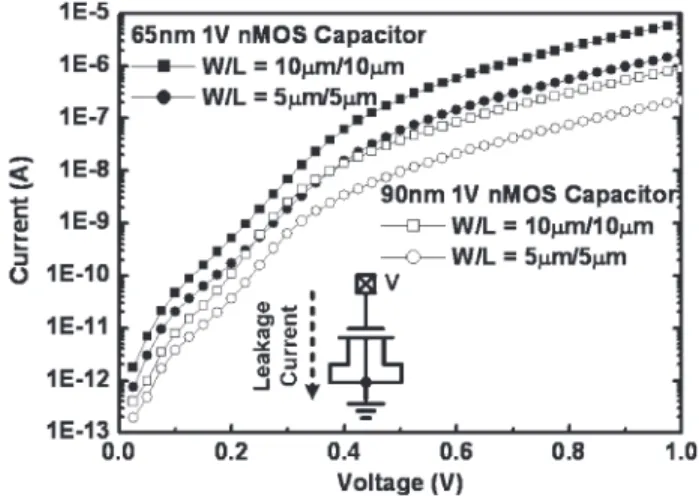
Fig. 1. Simulated gate currents of the nMOS capacitors in 65- and 90-nm CMOS technologies.
and the chip cost can be lowered. Recently, some works were reported on how to reduce the gate-leakage current by circuit technique for saving total power consumption in advanced CMOS technologies [6], [7].
The gate current of the MOSFET is directly dependent on the poly-gate area and the gate oxide thickness, which has been modeled in the BSIM4 MOSFET model [8]. Based on the corresponding SPICE parameters provided from the foundry, the gate current flowing through an nMOS capacitor with W/L of 5 μm/5 μm under 1-V bias is as large as 1.61 μA (217 nA) in a 65-nm (90-nm) CMOS technology. The simulated voltage-dependent gate-leakage currents of the nMOS capacitors are shown in Fig. 1, where the gate leakage issue in the 65-nm CMOS technology is obviously worse than that in the 90-nm CMOS technology.
Recently, some designs of the low-leakage power-rail elec-trostatic discharge (ESD) clamp circuit in nanometer CMOS technologies were revealed [9]–[11]. In [9], the gate current was utilized to bias the ESD detection circuit and to reduce the voltage difference across the gates of the MOS capacitors. In [10], the RC-based ESD detection circuit and the feedback con-trol inverter were used to avoid the direct leakage path through the MOS capacitor. In [11], the ESD detection circuit consisted of the RC timer, the inverters, and the feedback pMOS. The feedback pMOS could lower the voltage drop across the RC timer to reduce the gate-leakage current of the MOS capacitor. Other high-voltage-tolerant power-rail ESD clamp circuits had been also reported to solve the gate oxide reliability in the ESD
Fig. 2. Simulated node voltages of the traditional RC-based power-rail ESD clamp circuit [16] and the gate current flowing through MOS capacitor Mc under the normal power-on condition with a rise time of 1 ms in a 65-nm CMOS process.
protection circuit [12]–[15]. For [12] and [13], the substrate-triggered circuit, which is composed of the two pMOS devices, is controlled by the two RC-based detection circuits. In [14] and [15], the diode-connected pMOS was used as the voltage divider to bias the ESD detection circuit. However, those prior designs [12]–[15] did not consider the gate-leakage current if such circuits were further implemented in nanometer CMOS processes.
In this paper, a new power-rail ESD clamp circuit with ultralow standby leakage current and area efficiency is proposed and successfully verified in a 65-nm CMOS technology. The embedded ESD detection circuit realized with only thin gate oxide devices (1-V devices) can improve the turn-on efficiency of the ESD clamp device. By using the new proposed circuit solution, the standby leakage current of the proposed power-rail ESD clamp circuit can be significantly reduced to the order of nanoamperes under the normal circuit operating condition with 1-V bias.
II. ISSUE OFGATE-LEAKAGECURRENT IN THE
POWER-RAILESD CLAMPCIRCUIT
A. TraditionalRC-Based Power-Rail ESD Clamp Circuit The traditional RC-based power-rail ESD clamp circuit with a large-sized ESD clamp device was traditionally used to pro-tect the core circuits [16], as shown in the inset of Fig. 2. The simulated voltages on the nodes of the traditional RC-based power-rail ESD clamp circuit and the gate current of the MOS capacitor Mc are shown in Fig. 2, under the normal power-on cpower-onditipower-on with a rise time of 1 ms in a 65-nm 1-V CMOS process. The dimensions of R, Mc, Mp, Mn, and MESD are
165.3 kΩ, 64 μm/2 μm, 184 μm/60 nm, 36 μm/60 nm, and 2000 μm/0.1 μm, respectively. From the simulated results in Fig. 2, the gate current of Mc is 1.65 μA when VDD is raised up to 1 V. The voltage level on node A is about 0.72 V due to the voltage drop across R. Therefore, a leakage current path is generated from VDD through the inverter (Mp and Mn) to VSS. Consequently, the main ESD clamp device MESDoperating in
Fig. 3. Simulated node voltages of the capacitor-less power-rail ESD clamp circuit [17], the drain current, and the gate current flowing through the clamp device MESDunder the normal power-on transition.
the subthreshold region will cause more leakage current under the normal circuit operating condition.
B. Capacitor-Less Design of Power-Rail ESD Clamp Circuit Based on the concept of capacitor-less design [17], a silicon-controlled rectifier (SCR) clamp with a dual-base ESD detec-tion driver was proposed to save the area [18]. The SCR used as a ESD clamp device can reduce the leakage current. However, the gate leakage issue of the dual-base ESD detection driver in the advanced nanoscale CMOS process should be further considered.
The capacitor-less design of the power-rail ESD clamp cir-cuit with a large-sized ESD clamp device was proposed to protect the core circuits [17], as shown in the inset of Fig. 3. The simulated voltages on the nodes of the capacitor-less design of the rail ESD clamp circuit under the normal power-on cpower-onditipower-on with a rise time of 1 ms in a 65-nm 1-V CMOS process are shown in Fig. 3. The gate and drain currents of MESD are also shown in Fig. 3. The dimensions of Rp, Rn,
Mp, Mn, and MESD are 20 kΩ, 40 kΩ, 24 μm/60 nm,
12 μm/60 nm, and 2000 μm/0.1 μm, respectively. The p+ junction area of diode Dn is 0.057 μm2. From the simulated
results in Fig. 3, the gate current of MESD is 1.69 μA when
VDD is raised up to 1 V. The voltage drop across Rp mainly induced by the gate current of MESD is about 55 mV, which
is not enough to turn Mn on. Therefore, the ESD detection circuit can be almost turned off. However, there is still a leakage current path from VDD through the main ESD clamp device MESDto VSS. As shown in Fig. 3, the drain current of MESDis
as large as 11.79 μA and is the major source of the total standby leakage current.
The measured standby leakage currents of the traditional RC-based and capacitor-less power-rail ESD clamp circuits in a 65-nm CMOS process at room temperature are shown in Fig. 4. The voltage of the VDD power line is from 0 to 1 V with the voltage step of 20 mV. When VDD is 1 V, the measured standby leakage currents of the RC-based and capacitor-less power-rail ESD clamp circuits at room temperature are 760.42
Fig. 4. Measured standby leakage currents of the traditional RC-based and the capacitor-less power-rail ESD clamp circuits.
TABLE I
LEAKAGECURRENTS OF THEPOWER-RAILESD CLAMPCIRCUITS
UNDERDIFFERENTTEMPERATURES AT1 VIN A65-nm CMOS PROCESS
and 12.86 μA, respectively. The standby leakage currents of the traditional RC-based and capacitor-less power-rail ESD clamp circuits under different temperatures are also listed in Table I. Based on the measured results in Fig. 4 and Table I, the MOS transistor, which is drawn with large device dimension as the ESD clamp device, is too leaky for the portable products requiring low power consumption.
III. NEWPROPOSEDPOWER-RAILESD CLAMPCIRCUIT
A. Circuit Schematic
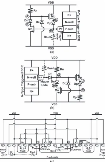
The new proposed power-rail ESD clamp circuits of the ultralow standby leakage are shown in Fig. 5(a) and (b), respec-tively, with p- and n-type triggered SCR devices as the main ESD clamp devices. In Fig. 5(c), the cross-sectional view of the proposed area-efficient power-rail ESD clamp circuit with an embedded ESD-transient detection circuit is shown. The main concept of layout modification is to sufficiently utilize parasitic elements in the ESD-transient detection circuit. By following this main concept, the layout area can be greatly saved due to not using additional resistors and capacitors. The SCR device [19] used as the main ESD clamp device can avoid the gate-leakage current issue due to not having a poly-gate structure inside the SCR device. However, the SCR device has some disadvantages, such as the slow turn-on speed and the high trig-gered voltage. Therefore, the ESD detection circuit is necessary to improve the turn-on speed of the SCR device under the ESD stress condition. The new proposed ESD detection circuit is designed with considerations of the gate-leakage current and the gate oxide reliability. By inserting the diode in the ESD detection circuit, the voltage differences across the gate oxide of the nMOS and pMOS transistors can be intentionally reduced.
Fig. 5. Proposed ultralow standby leakage power-rail ESD clamp circuits with the (a) p- and (b) n-type triggered SCR devices, as the ESD clamp devices, and (c) the embedded ESD-transient detection circuit in the cross-sectional view.
Therefore, the gate-leakage current of the nMOS and pMOS transistors in the ESD detection circuit can be well controlled to minimize the total standby leakage current.
In the proposed ESD detection circuit of Fig. 5(a), the pMOS Mp is used to generate the trigger current into the trigger node [node C in Fig. 5(a)] of the p-type triggered SCR device during the ESD stress event. Under the normal circuit operating condition, Mp is kept off, and the trigger node is kept at VSS through the parasitic p-substrate resistor Rsub. Therefore, the p-type triggered SCR device is turned off during the normal circuit operating condition.
The RC-based ESD-transient detection mechanism is real-ized by Rn and the junction capacitance of the reverse-biased diode Dc, which can distinguish the ESD stress event from the normal power-on condition. Compared with the thin gate oxide of the MOS in the traditional RC circuit, the reverse-biased diode Dc used as capacitor to realize the RC time constant in the proposed ESD detection circuit can be free from the gate-leakage current issue. The inserted diodes Dn and Dp in the ESD detection circuit are used to reduce the voltage differences across the gate oxide of transistors Mp and Mn in the ESD detection circuit. Therefore, the leakage current and the gate oxide reliability of Mp and Mn can be safely relieved.
to the gate of Mp and Mn are implemented by the parasitic resistance in the n-well and the p-substrate, respectively. The RC-based ESD-transient detection mechanism is realized by the Rwell and the reverse-biased diode Dc, which is imple-mented by the n-well/p-substrate junction of the surrounding guard ring. The inserted diodes Dn and Dp in the ESD-transient detection circuit are intentionally placed between the p+ pickup regions and the cathodes of SCR paths. This arrangement can increase the parasitic resistance of Rsub, and the trigger (hold-ing) voltage of the SCR device can be reduced in response to the increased value of Rsub. An additional n+ region connected to VDD is inserted to form diode Dr to provide a forward-biased discharging path from VSS to VDD during the ESD stress event.
B. Operation Under the Normal Power-On Transition
Under the normal circuit operation condition with VDD of 1 V and grounded VSS, the gate voltage of Mp (node A in Fig. 5) is biased at 1 V through resistor Rn in the new proposed ESD detection circuit. The gate voltage of Mn (node C) is simultaneously biased at 0 V through the parasitic p-substrate resistor Rsub (the resistor Rp) in the p-type (n-type) triggered design. Because Mp (Mn) is kept off, no trigger current is generated into (conducted from) the trigger node of the p-type (n-type) triggered SCR device. By inserting diodes Dp and Dn in the ESD detection circuit, the voltages at nodes B and D can be clamped to the desired higher or lower voltage levels. Therefore, the drain-to-gate and drain-to-source voltages of Mp and Mn can be far less than 1 V to further reduce the standby leakage current.
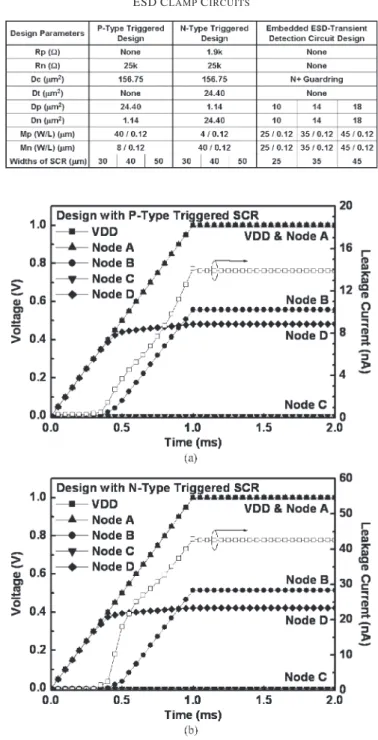
By using the SPICE parameters provided from foundry and the design dimensions listed in Table II, the simulated voltage waveforms and the leakage current of the proposed ESD detection circuit during the normal power-on transition are shown in Fig. 6, where VDD is raising from 0 to 1 V with a rise time of 1 ms. From the simulation results in Fig. 6, the voltage differences across the gate-to-drain, gate-to-source, and drain-to-source terminals of all transistors in the proposed ESD detection circuit are only about 0.5 V. Because Mp (Mn) with the device dimension of 40 μm/0.12 μm is used to trigger the p-type (n-type) triggered SCR device on during the ESD stress event and pMOS Mp has smaller gate-leakage current as compared to that of nMOS Mn in the same 65-nm CMOS
Fig. 6. Simulated voltage waveforms on the nodes and the leakage current of the ESD detection circuit with the (a) p- and (b) n-type triggered SCR devices in the 65-nm 1-V CMOS process under the normal power-on transition.
process, the simulated leakage current of the ESD detection circuit is around 13.9 nA (42.6 nA) for the p-type (n-type) triggered design, as shown in Fig. 6.
C. Operation Under the ESD Transition
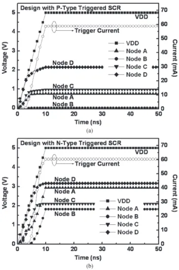
When a positive fast-transient ESD-like voltage is applied to VDD with grounded VSS, the RC time delay keeps node A at a relatively low voltage level as compared with that at VDD.
Fig. 7. Simulated voltages on the nodes and the trigger current of the ESD detection circuit with the (a) p- and (b) n-type triggered SCR devices in the 65-nm CMOS process under the ESD-like transition.
Mp can be quickly turned on to generate the trigger current into the trigger node (node C) of the p-type triggered SCR device in Fig. 5(a) and (c). The turned-on Mp can also elevate the voltage level at node C to further turn Mn on. When Mn is turned on, the trigger current can be conducted from the trigger node of the n-type triggered SCR device in Fig. 5(b) and (c).
To simulate the fast transient edge of the human-body-model (HBM) ESD event [20] before the breakdown on the internal devices to be protected, a 5-V voltage pulse with a rise time of 10 ns is applied to VDD. The simulated transient voltage and the trigger current of the ESD detection circuit during such an ESD-like transition are illustrated in Fig. 7. According to the simulation results, Mp (Mn) can be successfully turned on to generate (conduct) the trigger current for the p-type (n-type) triggered design. Finally, the SCR device is fully turned on to discharge the ESD current from VDD to VSS.
IV. EXPERIMENTALRESULTS
The new proposed power-rail ESD clamp circuits have been fabricated in a 65-nm CMOS process. All devices in the proposed design are 1-V fully silicided devices, including the SCR device. For p- and n-type triggered designs, the widths
Fig. 8. Microphotograph of the fabricated power-rail ESD clamp circuits with the (a) p- and (b) n-type triggered SCR devices, as the ESD clamp devices, and (c) the embedded ESD-transient detection circuit.
of SCR devices are split with 30, 40, and 50 μm to verify the corresponding ESD robustness. The device dimension of Mp (Mn) in the ESD detection circuit can be adjusted to provide different trigger currents for turning on the p-type (n-type) triggered SCR devices. Therefore, the gate widths of Mp and Mn are split with 40, 60, and 80 μm to investigate the turn-on efficiency of the proposed power-rail ESD clamp circuit. For the embedded ESD-transient detection circuit design, the widths of SCR devices are also split with 25, 35, and 45 μm. The widths of Mp and Mn are varied in response to the width of SCR device due to the embedded feature of the layout structure. Therefore, the widths of Mp and Mn would be 25, 35, and 45 μm for a single finger. For simplicity, the dimensions of Dp and Dn are also varied in response to the width of the SCR device, as listed in Table II. The reverse-biased diode Dc is provided by the surrounding n+ guard ring. These power-rail ESD clamp circuits are fabricated for the measurements of the transmission-line pulsing (TLP), the ESD test, the dc I−V curve, and the turn-on verification.
The microphotograph of the fabricated power-rail ESD clamp circuits are shown in Fig. 8(a)–(c) for the p-type trig-gered design, the n-type trigtrig-gered design, and the embedded ESD-transient detection circuit design, respectively.
A. TLP Measurement and ESD Robustness
In order to investigate the protection performance of the power-rail ESD clamp circuit during the ESD stress events,
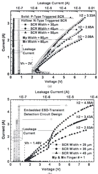
Fig. 9. TLP measured I−V curves of the fabricated power-rail ESD clamp circuits with the SCR devices of different widths under positive VDD-to-VSS ESD stress, (a) the p- and n-type triggered SCR designs, and (b) the embedded ESD-transient detection circuit design.
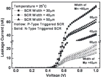
the TLP generator [21] with a pulsewidth of 100 ns and a rise time of ∼2 ns is used to measure the second breakdown current (It2) of the fabricated power-rail ESD clamp circuits. The TLP measured I−V curves of the fabricated power-rail ESD clamp circuits with different SCR widths are shown in Fig. 9(a) for the p- and n-type triggered designs and in Fig. 9(b) for the embedded ESD-transient detection circuit design at room temperature. The power-rail ESD clamp circuit with p-type (n-type) triggered SCR widths of 30, 40, and 50 μm can achieve the It2 values of 2.07, 2.65, and 3.33 A (2.08, 2.65, and 3.32 A), respectively. In Fig. 9, the It2 value of the embedded ESD-transient detection circuit design is about 1.30 times the value of p- and n-type triggered designs because the embedded ESD-transient detection circuit design can provide two SCR discharging paths. The trigger voltage of the fabricated power-rail ESD clamp circuit with different Mp (Mn) widths is shown in Fig. 10. As shown in Fig. 10, the trigger voltage can be obviously reduced when the Mp (or Mn) width is increased. Therefore, the turn-on speed of the SCR device can be properly
Fig. 10. TLP measured trigger voltage of the p- and n-type triggered design with different widths of Mp, Mn, and SCR devices.
TABLE III
TLP MEASUREDCHARACTERISTICS ANDESD ROBUSTNESS OF THE
FABRICATEDPOWER-RAILESD CLAMPCIRCUITS
adjusted by the dimension of Mp or Mn to meet different application requirements. In addition, the holding voltages (Vh) of the p- and n-type triggered designs are around∼2 V. The Vh value of the embedded ESD-transient detection circuit design is around∼1.46 V due to larger Rsub and Rwell in the layout structure. The ESD clamp circuit with lower Vh has better ESD protection capability. The fabricated power-rail ESD clamp circuits with Vh higher than VDD of 1 V are free to latchup issues for 1-V applications [22], [23].
The HBM and machine-model (MM) [24] ESD levels of the fabricated power-rail ESD clamp circuit under positive VDD-to-VSS ESD stress are listed in Table III. The HBM and MM ESD levels of the proposed power-rail ESD clamp circuits are also only related to the width of the SCR device. From the measured results, the HBM ESD levels of the embedded ESD-transient detection circuit design are about 1.1 times the values of p- and n-type triggered designs. The other TLP measured characteristics of the fabricated power-rail ESD clamp circuit are also listed in Table III.
Fig. 11. Measured dc I–V curves of the fabricated power-rail ESD clamp circuits with SCR devices of different widths.
TABLE IV
MEASUREDLEAKAGECURRENTS OF THEFABRICATEDPOWER-RAIL
ESD CLAMPCIRCUITSUNDERDIFFERENTTEMPERATURES AT1 V
B. Standby Leakage Current Measurement
The leakage current of the fabricated power-rail ESD clamp circuits are measured by HP4155 from 0 to 1 V with the voltage step of 20 mV, as shown in Fig. 11. In Fig. 11, the standby leakage currents of the power-rail ESD clamp circuits with SCR widths of 30, 40, and 50 μm are similar, because the leakage current in the SCR device is quite small. When the device dimension of Mp (Mn) increases from 40 μm/0.12 μm to 80 μm/0.12 μm, the standby leakage current of the power-rail ESD clamp circuit with a p-type (n-type) triggered SCR of 50 μm increases from 16.4 to 24.8 nA (42.9 to 84.3 nA) at 25◦C under 1-V bias. The standby leakage currents of the fabricated power-rail ESD clamp circuits at room temperature are reduced to the order of nanoamperes only, because the gate oxide leakage is successfully relieved by inserting the diodes in the ESD detection circuit. The n-type triggered design has the largest standby leakage current because the nMOS Mn has larger gate-leakage current as compared to that of the pMOS at the same device size in the 65-nm CMOS process. Increasing the device dimension of Mp (Mn) results in a larger standby leakage current under the normal circuit operating condition, but at the same time, it can increase the trigger current to improve the turn-on speed of the triggered SCR device with a reduced trigger voltage (as shown in Fig. 10 and Table III). The measured results of the standby leakage current at 1-V normal
Fig. 12. Measured voltage and current waveforms of the fabricated power-rail ESD clamp circuits with the SCR devices under the TLP transition, the (a) p- and (b) n-type triggered SCR devices, and (c) the embedded ESD-transient detection circuit design.
operating voltage under different temperatures are also listed in Table IV.
C. Turn-On Verification
In order to observe the turn-on behavior of the fabricated power-rail ESD clamp circuits, a TLP voltage pulse with a rise
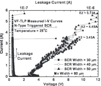
Fig. 13. VF-TLP measured I–V curves of the fabricated power-rail ESD clamp circuits with the n-type triggered SCR device of different widths under positive VDD-to-VSS ESD stress. The VF-TLP is with a pulsewidth of 10 ns and a rise time of 200 ps.
time of 2 ns and a pulse height of 20 V is applied to the VDD power line with the grounded VSS. The TLP voltage pulse will start the ESD detection circuit to generate the trigger current to trigger on the SCR device. The triggered-on SCR device can provide a low impedance path from VDD to VSS to discharge the ESD current. When the TLP voltage pulse height of 20 V is applied to VDD, the p-type (n-type) triggered SCR can be fully turned on to be a low impedance path, and the voltage across the clamp circuit is clamped to only 2.5 V in Fig. 12(a) [2.2 V in Fig. 12(b)]. However, the power-rail ESD clamp circuit with the embedded ESD-transient detection circuit can be also activated to clamp the voltage down to the lower level of 1.84 V (2.08 V) for the SCR width in 45 μm (25 μm) due to two SCR discharging paths, as shown in Fig. 12(c).
The charged device model (CDM) is also an important ESD testing standard for ICs. In order to investigate the turn-on behavior of the proposed designs under the CDM-like fast transient condition, the very fast (VF) TLP with a pulsewidth of 10 ns and a rise time of 200 ps is used to measure the fabricated power-rail ESD clamp circuits. The VF-TLP measured I−V curves of the power-rail ESD clamp circuits with different SCR widths are shown in Fig. 13 for the n-type triggered SCR, where the device dimension of Mn is kept at 80 μm/0.12 μm. In Fig. 13, the power-rail ESD clamp circuit with n-type triggered SCR widths of 50 μm can achieve the It2 value of 5.73 A (3.33A) for the VF-TLP (TLP) measurement. It can be observed that the SCR device with a larger device width has smaller turn-on resistance to effectively discharge the ESD current.
V. CONCLUSION
A new design of the power-rail ESD clamp circuit to achieve ultralow standby leakage current and area efficiency has been proposed and successfully verified in a 65-nm fully silicided CMOS technology. The new proposed ESD detection circuit has been realized with only 1-V devices without suffering the gate leakage issue. According to the measured results, the
ACKNOWLEDGMENT
The authors would like to thank Y.-C. Liang of Industrial Technology Research Institute (ITRI) for his valuable technical discussion and suggestion. The authors would also like to express their thanks to T. Hasebe, K. Hasegawa, and M. Sawada for the help of VF-TLP measurement from Hanwa Electronic Ind. Co., Ltd., Japan.
REFERENCES
[1] M. Luisier and A. Schenk, “Two-dimensional tunneling effects on the leakage current of MOSFETs with single dielectric and high-k gate stacks,” IEEE Trans. Electron Devices, vol. 55, no. 6, pp. 1494–1501, Jun. 2008.
[2] P. J. Wright and K. C. Saraswat, “Thickness limitations of SiO2 gate
dielectrics for MOS ULSI,” IEEE Trans. Electron Devices, vol. 37, no. 8, pp. 1884–1892, Aug. 1990.
[3] Y.-Y. Fan, Q. Xiang, J. An, L. F. Register, and S. K. Banerjee, “Impact of interfacial layer and transition region on gate current performance for high-K gate dielectric stack: Its tradeoff with gate capacitance,” IEEE
Trans. Electron Devices, vol. 50, no. 2, pp. 433–439, Feb. 2003.
[4] J. Huang, P. D. Kirsch, J. Oh, S. H. Hoon, P. Majhi, H. R. Harris, D. C. Gilmer, G. Bersuker, D. Heh, C. S. Park, C. Park, H.-H. Tseng, and R. Jammy, “Mechanisms limiting EOT scaling and gate leakage of high- k/metal gate stacks directly on SiGe,” IEEE Electron Device Lett., vol. 30, no. 3, pp. 285–287, Mar. 2009.
[5] M.-D. Ker, S.-L. Chen, and C.-S. Tsai, “Overview and design of mixed-voltage I/O buffers with low-mixed-voltage thin-oxide CMOS transistors,” IEEE
Trans. Circuits Syst. I, Reg. Papers, vol. 53, no. 9, pp. 1934–1945,
Sep. 2006.
[6] D. Lee, D. Blaauw, and D. Sylvester, “Static leakage reduction through simultaneous Vt/Tox and state assignment,” IEEE Trans.
Comput.-Aided Design Integr. Circuits Syst., vol. 24, no. 7, pp. 1014–1029,
Jul. 2005.
[7] A. K. Sultania, D. Sylvester, and S. S. Sapatnekar, “Gate oxide leakage and delay tradeoffs for dual- Toxcircuits,” IEEE Trans. Very Large Scale
Integr. (VLSI) Syst., vol. 13, no. 12, pp. 1362–1375, Dec. 2005.
[8] BSIM Model, Berkeley Short-Channel IGFET Model. [Online]. Avail-able: http://www-device.eecs.berkeley.edu/bsim
[9] C.-T. Wang and M.-D. Ker, “Design of power-rail ESD clamp cir-cuit with ultra-low standby leakage current in nanoscale CMOS tech-nology,” IEEE J. Solid-State Circuits, vol. 44, no. 3, pp. 956–964, Mar. 2009.
[10] P.-Y. Chiu, M.-D. Ker, F.-Y. Tsai, and Y.-J. Chang, “Ultra-low-leakage power-rail ESD clamp circuit in nanoscale low-voltage CMOS process,” in Proc. IEEE Int. Rel. Phys. Symp., 2009, pp. 750–753.
[11] M.-D. Ker and C.-Y. Lin, “High-voltage-tolerant ESD clamp circuit with low standby leakage in nanoscale CMOS process,” IEEE Trans. Electron
Devices, vol. 57, no. 7, pp. 1636–1641, Jul. 2010.
[12] M.-D. Ker and K.-H. Lin, “Overview on electrostatic discharge protection designs for mixed-voltage I/O interfaces: Design concept and circuit im-plementations,” IEEE Trans. Circuits Syst. I, Reg. Papers, vol. 53, no. 2, pp. 235–246, Feb. 2006.
[13] M.-D. Ker and W.-J. Chang, “ESD protection design with on-chip ESD bus and high-voltage-tolerant ESD clamp circuit for mixed-voltage I/O
complementary substrate-triggered SCR devices,” IEEE J. Solid-State
Circuits, vol. 38, no. 8, pp. 1380–1392, Aug. 2003.
[20] Electrostatic Discharge Sensitivity Testing—Human Body Model (HBM)—Component Level, ESD Association Standard, Test Method
ESD STM5.1, 2001.
[21] T. J. Maloney and N. Khurana, “Transmission line pulsing techniques for circuit modeling of ESD phenomena,” in Proc. EOS/ESD Symp., 1985, pp. 49–54.
[22] M.-D. Ker and S.-F. Hsu, Transient-Induced Latchup in CMOS Integrated
Circuits. Hoboken, NJ: Wiley, 2009.
[23] M.-D. Ker and S.-F. Hsu, “Physical mechanism and device simulation on transient-induced latchup in CMOS ICs under system-level ESD test,” IEEE Trans. Electron Devices, vol. 52, no. 8, pp. 1821–1831, Aug. 2005.
[24] Electrostatic Discharge Sensitivity Testing—Machine Model (MM)—Component Level, ESD Association Standard, Test Method
ESD STM5.2, 1999.
Ming-Dou Ker (F’08) received the Ph.D. degree
from the Institute of Electronics, National Chiao-Tung University (NCTU), Hsinchu, Taiwan, in 1993. He is currently a Distinguished Professor with the Department of Electronics Engineering, NCTU. Since 2012, he is serving as the Editor of IEEE
![Fig. 2. Simulated node voltages of the traditional RC-based power-rail ESD clamp circuit [16] and the gate current flowing through MOS capacitor Mc under the normal power-on condition with a rise time of 1 ms in a 65-nm CMOS process.](https://thumb-ap.123doks.com/thumbv2/9libinfo/7769002.150025/2.891.447.822.101.355/simulated-voltages-traditional-circuit-current-flowing-capacitor-condition.webp)