國 立 交 通 大 學
材料科學與工程學系
博士論文
銅內連線及低介電常數材料製程整合於高介電
常數薄膜電容
Integration of High-k MIM Capacitors with Copper
Interconnect and Low-k Dielectric
研 究 生: 蔡國強
指導教授: 朝春光 教授
吳文發 博士
銅內連線及低介電常數材料製程整合於高介電常數薄膜電
容
Integration of High-k MIM Capacitors with Copper Interconnect
and Low-k Dielectric
研 究 生: 蔡國強 Student: Kou-Chiang Tsai
指導教授: 朝春光 教授 Advisors: Dr. Chuen-Guang Chao
吳文發 博士 Dr. Wen-Fa Wu
國立交通大學
材料科學與工程學系
博士論文
A Thesis
Submitted to Department of Materials Science and Engineering
College of Engineering
National Chiao Tung University
in Partial Fulfillment of the Requirements
for the Degree of Doctor of Philosophy
in
Materials Science and Engineering
May 2006
Hsinchu, Taiwan, Republic of China
銅內連線及低介電常數材料製程整合於高介電常數薄膜電
容
研究生: 蔡國強 指導教授: 朝春光 教授 吳文發 博士 國立交通大學 材料科學與工程學系 博士論文摘要
本研究探討及研發具有高效能及穩定性的銅金屬內連線於先進高介電常數 金屬-絕緣層-金屬(MIM)薄膜電容元件應用。以金屬鋁/鉭/金屬銅/鉭 (Al/Ta/Cu/Ta) 作為Ta2O5薄膜電容的底電極,可降低漏電流密度至1x10⁻⁹ A/cm2並提升崩潰電 壓至5.2 MV/cm。因金屬鋁自身形成緻密且均勻氧化鋁,所以超薄金屬鋁成功地 阻絕 Ta2O5 中的氧熱擴散至金屬銅層形成氧化銅。此外以低溫短時間的高密度 N2O 電漿處理 Ta2O5薄膜能有效提升電容效能及元件熱穩定性,降低漏電流密度 至4x10⁻¹⁰ A/cm2。 本研究並研究高介電常數材料鈦酸鍶鋇薄膜(BST)於先進 MIM 薄膜電容的 應用。以銅鎂合金[Cu(Mg)]取代金屬銅成為金屬電極,因退火後會生成超薄 MgO 薄膜,能阻絕氧擴散,所以大幅降低漏電流密度。以氮化鉭/銅/氮化鉭(TaN/Cu/TaN) 為電極應用於先進高介電常數BST MIM 電容,結果顯示電容元件具有超高電容 密度(11.5 fF/µm2)。此外,高介電常數材料 BST 薄膜蝕刻及圖型定義亦是研究重點。以氯為反應氣體雖能有效蝕刻 BST 薄膜,但會殘留含鋇及鍶的化合物,降 低元件電容特性。本實驗以氧電漿做蝕刻後處理能修補因蝕刻所造成的薄膜缺 陷,降低漏電流密度至3.0×10⁻⁸ A/cm2及提升崩潰電場強度至2 MV/cm。 本實驗亦研究銅導線系統中,擴散阻障層與低介電常數材料 SiOC:H 薄膜間 的交互作用及穩定性分析,藉銅離子漂移程度探討擴散阻障層效能及元件穩定 性。因為在以金屬銅為電極的金屬層-絕緣層-半導體(MIS)結構中,施加正電場 於金屬銅會使其分解為銅離子加速擴散至元件中。因此,高穩定性的 MIS 的結 構是以金屬銅/氮化鉭/金屬鉭(Cu/TaN/Ta)多層薄膜為電極。此外,研究 N2O 電漿 後處理對擴散阻障層氮化鎢及金屬鎢薄膜的阻障效能影響。結果顯示經電漿後處 理的擴散阻障層具有奈米結構表面,能增加元件熱穩定性及阻障效能。本研究並 以Whipple 及 Fick’s 第二定律深入分析銅擴散在擴散阻障層的晶粒及晶界擴散因 子。
Integration of High-k MIM Capacitors with Copper
Interconnect and Low-k Dielectric
Student: Kou-Chiang Tsai Advisor: Dr. Chuen-Guang Chao Dr. Wen-Fa Wu
A Dissertation
Department of Materials Science and Engineering National Chiao Tung University
Abstract
We have investigated the characteristics and reliability of high dielectric constant metal-insulator-metal capacitors with copper interconnects. The properties of tantalum oxide (Ta2O5) metal-insulator-metal (MIM) capacitors with Al/Ta/Cu/Ta bottom electrodes were investigated. An ultra thin Al film successfully suppresses oxygen diffusion in the Ta2O5 MIM capacitor with the Cu-based electrode. The decrease in leakage current is attributed to formation of a dense and uniform Al2O3 layer, which has self-protection property and stops further oxygen diffusion into the tantalum contact. Moreover, the electrical characteristics of Ta/Ta2O5/Ta capacitors are improved by the treatments with inductively coupled N2O plasma.
To integrate the high dielectric constant (Ba,Sr)TiO3 (BST) film in the advanced MIM capacitor, Cu(Mg) alloy films have replaced pure Cu films as bottom electrodes for BST capacitors used in high-frequency devices. High-quality characteristics probably follow the formation of a self-aligned MgO layer following the deposition of
a Cu(Mg) alloy by annealing in an oxygen ambient, yielding an electrode with an excellent diffusion barrier and electrical characteristics, which is therefore effective in a BST thin-film capacitor. MIM capacitors made from a BST high-k dielectric film with Cu-based electrodes were also fabricated and demonstrated. The MIM capacitor has a high capacitance density of 11.5 fF/μm2, a low dissipation factor below 0.03 and small frequency dependence. Furthermore, BST thin films were patterned for fabricating BST capacitors in a helicon-wave plasma system. Some etching residues consisting of Ba and Sr were found after the BST films were etched and increased leakage current density. Oxygen surface plasma treatment can effectively repair surface damage caused by etching, and reduce the leakage current density and increase the breakdown field of the BST capacitor.
To study the high performance Cu metallization in ULSI technology, the interactions between low-k material SiOC:H and barrier layers have been investigated. The drift mobility of the Cu+ ions in the Cu/TaN/Ta-gated capacitor was lower than that in a Cu-gated capacitor. The electric field in the Cu-gated MIS capacitor in the cathode region is believed to be increased by the accumulation of positive Cu+ ions, which determines the breakdown acceleration. Good Cu+ ions drift barrier layers are required as reliable interconnects using thin TaN and Ta layers. Thermal stabilities of Cu-contacted n+-p junctions with tungsten nitride (WNx) diffusion barriers deposited at various nitrogen flow ratios are investigated. N2O plasma treatment is applied to improve thermal stability and barrier performance of WNx film. Meanwhile, N2O plasma-treated W barrier has a nanostructured surface layer and shows high thermal stability and best barrier properties. Also investigated herein are the lattice and grain boundary diffusivities extracted from the Cu penetration depth profiles using the Whipple analysis of grain boundary diffusion and Fick’s second law of diffusion.
Contents
Abstract (Chinese) I
Abstract (English) III
Contents V
Table Captions IX
Figure Captions X
Chapter 1 Organization of the Thesis
1Chapter 2 High Reliability and Performance Ta
2O
5MIM Capacitor
with Cu-based Electrodes
2.1 Introduction 3
2.1.1 Enhancement on the Cu-based Electrode 3
2.1.2 Improvement on the Ta2O5 Film 4
2.2 Device Fabrication and Characteristics Measurement 7 2.2.1 MIM Capacitor with Cu-based Electrode 7 2.2.2 MIM Capacitor using Low-temperature ICP-N2O Plasma 7
2.2.3 Characteristics Measurement 8
2.3 Results and Discussion 10
2.3.1 Ta2O5 MIM Capacitor with Cu-based Electrode 10
2.3.1-1 Physical Characteristic 10
2.3.1-2 Electrical Characteristics 11
2.3.1-3 Electrical Mechanism 12
2.3.1-4 Device Lifetime 15
2.3.2-1 Electrical Characteristic 16
2.3.2-2 Physical Characteristics 17
2.3.2-3 Plasma Treatment Mechanism 19
2.3.2-4 Device Lifetime 19
2.3.2-5 Electrical Mechanism 20
2.4 Summary 23
References 24
Chapter 3 High Performance and Reliability of High Dielectric
Constant (Ba,Sr)TiO
3Thin-Film Capacitor with Cu-based Electrodes
3.1 Introduction 50
3.1.1 Impact of a Cu(Mg) Bottom Electrode 51
3.1.2 Impact of Cu-based Electrodes 52
3.1.3 BST Etching Issue 52
3.2 Device Fabrication and Characteristics Measurement 54
3.2.1 MIM using a Cu(Mg) Electrode 54
3.2.2 MIM using Cu-based Electrodes 54
3.3.3 BST Etching Method 55
3.3.4 Characteristics Measurement 56
3.3 Results and Discussion 58
3.3.1 Improving the Electrical Properties and Thermal Stability of (Ba,Sr)TiO3 Thin
Films on Cu(Mg) Bottom Electrodes 58
3.3.1-1 Physical Characteristic 58
3.3.1-2 Electrical Characteristic 60
3.3.1-3 Device Thermal Stability 61
(Ba,Sr)TiO3 Thin-film Capacitors 64
3.3.2-1 Physical Characteristic 64
3.3.2-2 Electrical Characteristic 64
3.3.2-3 Frequency Effect 67
3.3.3 Repairing of Etching-induced Damage of High-k Ba0.5Sr0.5TiO3 Thin Films by
Oxygen Surface Plasma Treatment 69
3.4 Summary 74
References 76
Chapter 4 Impact of Diffusion Barrier Layers on Integration of
Low-k SiOC:H and Copper
4.1 Introduction 110
4.2 Device Fabrication and Characteristics Measurement 112
4.2.1 Experimental Methods 112
4.2.2 Characteristics Measurement 113
4.3 Results and Discussion 115
4.3.1 Influence of Ti, TiN, Ta and TaN Layers on Integration of Low-k SiOC:H and
Cu 115
4.3.1-1 Physical Property 115
4.3.1-2 Electrical Property 117
4.3.2 Influence of Bias-Temperature Stressing on the Electrical Characteristics of SiOC:H Film with Cu/TaN/Ta-gated Capacitor 119
4.3.2-1 Electrical characteristic 119
4.3.2-2 Electrical Mechanism 121
4.3.2-3 Device Lifetime 123
4.4 Summary 125
Reference 126
Chapter 5 Effect of Plasma Treatment on the Performance of
W-based Diffusion Barrier Layers for Cu Interconnection
5.1 Introduction 149
5.1.1 Influence of N2O Plasma Treatment on WNx Barriers 150 5.1.2 Analysis of Cu Diffusion in Plasma-treated Tungsten Barrier 150 5.2 Device Fabrication and Characteristics Measurement 152 5.2.1 Plasma-treatment on WNx Barrier Layer 152 5.2.2 Plasma-treatment on W Barrier Layer 152
5.2.3 Characteristics Measurement 153
5.3 Results and Discussion 154
5.3.1 Influence of N2O Plasma Treatment on Microstructure and Thermal Stability
of WNx Barriers for Cu Interconnection 154
5.3.2 Numerical and Experimental Analysis of Cu Diffusion in Plasma-treated
Tungsten Barrier 160
2.4 Summary 170
References 171
Table Captions
Chapter 2
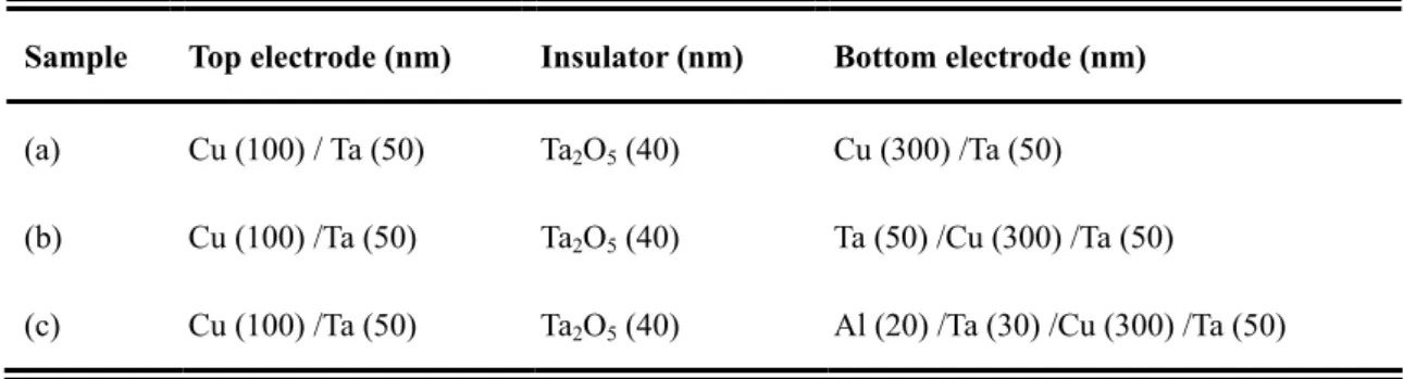
Table 2.1 MIM capacitors with various multilayered bottom electrodes used in the study.
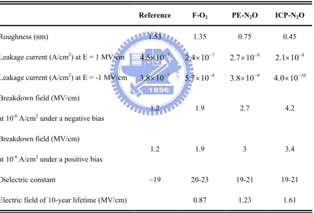
Table 2.2 MIM capacitors with various plasma treatments in the study. Table 2.3 Properties of Ta/Ta2O5/Ta capacitors with various post treatments.
Chapter 3
Table 3.1. Structures and thickness (nm) of BST MIM capacitors used in this study.
Chapter 5
Table 5.1 Table 5.1 Properties of tungsten nitride barriers deposited at various nitrogen flow ratios used in the study.
Table 5.2 Table 5.2 Properties of W, WN and W(N2O) diffusion barriers. Properties of sputtered Ta, Ti films are also listed for comparison. Leakage current densities of diodes were measured at a reverse bias of 5V after annealing at 600°C for 30 min.
Table 5.3 Table 5.3 Summary of the values of diffusivities, pre-exponential factors, and activation energies for Cu diffusion in W films at various annealing temperatures.
Table 5.4 Table 5.4 Summary of the values of diffusivities, and pre-exponential factors for Cu diffusion in W(N2O) films and at various annealing temperatures. Other barrier materials are also listed for comparison.
Figure Captions
Chapter 1
Figure 1.1 Schematic of MIM capacitor in the Cu-based BEOL.
Chapter 2
Figure 2.1 SEM images of the Ta2O5 films on (a) Ta/Cu/Ta and (b) Al/Ta/Cu/Ta bottom electrodes after annealing at 600oC for 30 min in oxygen ambient.
Figure 2.2 (a) SIMS depth profiles of O elements in the Ta2O5/Ta/Cu/Ta samples after furnace annealing at 500 and 600oC for 30 min in oxygen ambient. (b) High-resolution TEM image of the interlayer between Ta and Cu layers in the Ta2O5/Ta/Cu/Ta sample.
Figure 2.3 (a) SIMS depth profiles of O elements in Ta2O5/Al/Ta/Cu samples after furnace annealing at 500 and 600oC for 30 min in oxygen ambient. (b) High-resolution TEM image of the region between Ta and Cu layers in the Ta2O5/Al/Ta/Cu/Ta sample.
Figure 2.4 TEM image of the Cu/Ta/Ta2O5/Al/Ta/Cu/Ta MIM capacitor. The annealing was conducted at 600oC for 30 min in oxygen ambient after Ta2O5 film was deposited.
Figure 2.5 O 1s XPS spectra obtained from (a) Ta2O5-Ta interface for the Ta2O5/Ta/Cu/Ta sample and (b) Ta2O5-Al interface for the Ta2O5/Al/Ta/Cu/Ta sample.
Figure 2.6 Current density-electric field (J-E) characteristics of the Cu/Ta/Ta2O5/Al/Ta/Cu/Ta MIM capacitors after annealing at various temperatures in oxygen ambient for 30 min.
Figure 2.7 Current density-electric field (J-E) characteristics of the Ta2O5 MIM capacitors with various bottom electrodes after annealing at 600oC in oxygen ambient for 30 min.
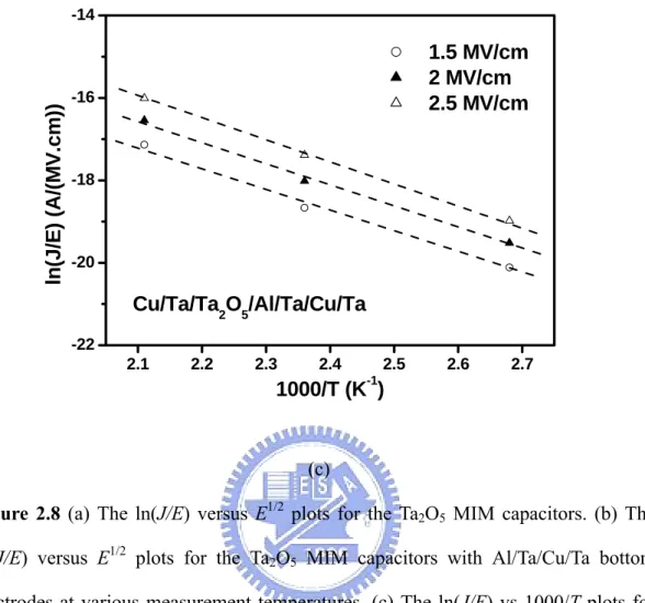
Figure 2.8 (a) The ln(J/E) versus E1/2 plots for the Ta2O5 MIM capacitors. (b) The ln(J/E) versus E1/2 plots for the Ta2O5 MIM capacitors with Al/Ta/Cu/Ta bottom electrodes at various measurement temperatures. (c) The ln(J/E) vs 1000/T plots for the Ta2O5 MIM capacitors with Al/Ta/Cu/Ta bottom electrodes.
Figure 2.9 Schematic illustration of conduction mechanisms in Ta2O5 MIM capacitors with (a) Ta/Cu/Ta and (b) Al/Ta/Cu/Ta bottom electrodes biased at a positive voltage.
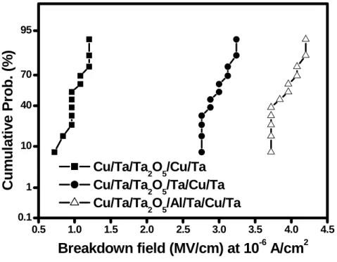
Figure 2.10 Cumulative probabilities of breakdown fields for Ta2O5 MIM capacitors with various bottom electrodes.
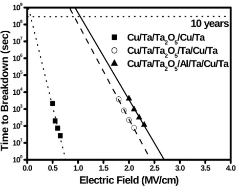
Figure 2.11 TDDB lifetime as a function of electric field for Ta2O5 MIM capacitors with various bottom electrodes.
Figure 2.12 Leakage current densities of the Ta/Ta2O5/Ta capacitors before and after various post treatments.
Figure 2.13 SIMS depth profiles of oxygen elements in Ta/Ta2O5/Ta capacitors after furnace annealing at 400°C for 30 min and ICP treatment at 250°C for 5 min.
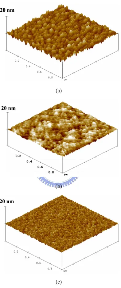
Figure 2.14 AFM images of Ta2O5 surfaces after (a) furnace annealing at 400°C for 30 min, (b) PE treatment at 250°C for 5 min, and (c) ICP treatment at 250°C for 5 min.
Figure 2.15 Schematic illustration for N2O plasma treatment on the Ta2O5 film. Figure 2.16 Leakage current density vs. time properties for F-O2 sample under 1.2
1.8 MV/cm.
Figure 2.17 The ln(J) versus E1/2 plots for various Ta/Ta2O5/Ta capacitors.
Figure 2.18 Schematic illustrations of conduction mechanisms in Ta/Ta2O5/Ta capacitors. (a) F-O2 and (b) ICP-N2O samples.
Chapter 3
Figure 3.1 Schematic diagram of BST MIM capacitor with Cu/TaN electrodes. Figure 3.2 XRD patterns of BST thin film deposited on (a) Cu, and (b) Cu(Mg)
bottom electrodes before and after annealing at 400°C for 30 min in an oxygen atmosphere in a furnace.
Figure 3.3 SEMs of BST thin film deposited on the Cu bottom electrode (a) before and (b) after annealing at 400°C for 30 min in oxygen atmosphere, and deposited on the Cu(Mg) electrode (c) before and (d) after annealing at 400°C for 30 min in oxygen atmosphere.
Figure 3.4 Schematic drawing presents Cu oxidation mechanism where the oxidation barrier fails.
Figure 3.5 Auger depth profiles of (a) BST/Cu and (b) BST/Cu(Mg) systems before and after furnace annealing at 400°C for 30 min in oxygen ambient. Figure 3.6 Cross-sectional TEM images of interface of the BST/Cu system after
furnace annealing at (a) 400 and (b) 500°C for 30 min in oxygen ambient, and which of the BST/Cu(Mg) system after furnace annealing at (c) 400 and (d) 500°C for 30 min in oxygen ambient.
Figure 3.7 J-E characteristics of the BST with Cu and Cu(Mg) electrodes before and after furnace annealing at 400 and 500°C for 30 min in oxygen ambient.
temperature range 100 to 200°C and an electrical field of up to 4 MV/cm.
Figure 3.9 J-E relations of BST/Cu(Mg) system before and after a constant 2V stress has been applied for 30 and 60 sec.
Figure 3.10 Time-dependent dielectric breakdown (TDDB) characteristics of BST capacitors with (a) Cu and (b) Cu(Mg) electrodes with an applied bias of 2V at room temperature (RT) and at 200°C.
Figure 3.11 SEM micrographs of BST film when deposited directly on the (a) Cu and (b) TaN/Cu bottom electrodes after annealing at 4000C for 30 min in O2.
Figure 3.12 Cross-sectional TEM image of BST MIM capacitors with Cu/TaN electrodes.
Figure 3.13 Leakage current density-electric field (J-E) characteristics of BST MIM capacitors with Cu-based electrodes at various annealing temperatures. Figure 3.14 ln(J) versus E1/2 for conduction mechanism of BST-4 capacitor,
representing Schottky emission at low electric field.
Figure 3.15 ln(J/E) versus E1/2 for conduction mechanism of BST-4 capacitor, representing Poole-Frenkel effect at high electric field.
Figure 3.16 (a) Characteristics of leakage current density against period of stress in constant electric field from 1.5 to 1.75 MV/cm for the BST-4 capacitor. (b) Projected life-time of BST capacitors with Cu-based electrodes. Figure 3.17 Capacitance densities and dissipation factors of BST-4 capacitor with
Cu/TaN electrodes as functions of frequency.
Figure 3.18 (a) Quadratic voltage coefficients α and (b) linear voltage coefficients β of capacitances of BST-4 capacitor with Cu/TaN electrodes as functions of frequency.
Figure 3.19 Normalized capacitances of BST-4 capacitor with Cu/TaN electrodes as a function of temperatures.
Figure 3.20 Etch rate of BST thin film as a function of (a) HWP power, and (b) substrate bias rf power.
Figure 3.21 Leakage current characteristics of the etched BST thin films with various (a) HWP power, and (b) substrate bias rf power.
Figure 3.22 Etch rate of BST thin films as a function of gas mixture.
Figure 3.23 (a) Ba 3d, (b) Sr 3d, and (c) Ti 2p XPS narrow scan spectra of the as-etched BST thin films with various Ar/Cl2 gas mixing ratio, and oxygen surface plasma treatment.
Figure 3.24 Leakage current characteristics of the as-etched and oxygen surface plasma treatment BST thin films.
Figure 3.25 SEM photographs of (a) the as-deposited BST thin film; as-etched BST thin films (b) before and (c) after oxygen surface plasma treatment. Figure 3.26 Rms roughness value of as-etched BST thin films as a function of Ar/Cl2
gas mixing ratio and oxygen surface plasma treatment sample: (a) as-deposited BST thin film, (b) pure Ar etched BST thin film, (c) (sample (b)) after oxygen surface plasma treatment, (d) Ar(80%)/Cl2(20%) etched BST thin film, and (e) (sample (d)) after oxygen surface plasma treatment.
Chapter 4
Figure 4.1 The structures of Cu/barrier/SiOC:H MIS capacitor.
Figure 4.2 Structures of (a) Cu-gated and (b) Cu/TaN/Ta-gated MIS capacitors in SiOC:H dielectrics.
the SiOC:H film.
Figure 4.4 Top-view SEM micrographs showing the surface morphology of the (a) CVD-Ti and (b) PVD-Ti capacitors.
Figure 4.5 Percentage variation in sheet resistance of diffusion barrier layers on SiOC:H/Si structures as a function of annealing temperatures range from 400 to 700ºC.
Figure 4.6 Experimental contact percentage of (a) C and (b) O results from the interaction of the barriers with SiOC:H before and after annealing at 400-600ºC, based on the AES.
Figure 4.7 AFM images of the (a) PVD-Ti, (b) PVD-TiN and (c) CVD-TiN MIS capacitors.
Figure 4.8 Breakdown field distributions of (a) as-deposited Cu/barrier/SiOC:H MIS capacitors and after annealing at (b) 400ºC and (c) 500ºC for 30 min.
Figure 4.9 C-V characteristics with Cu/barrier/SiOC:H MIS capacitor after BTS at 2 MV/cm and 250ºC for the (a) PVD-TiN, (b) CVD-TiN and (c) TaN layer. Figure 4.10 Flatband voltage shift ∆VFB[Cu+] of Cu+ ions versus BTS temperature
under various stress time at 1.5 MV/cm.
Figure 4.11 Arrhenius plot of estimated drift mobility of Cu+ ions in the SiOC:H dielectrics versus 1000/T.
Figure 4.12 Leakage current density-electric filed characteristics of (a) Cu-gated and (b) Cu/TaN/Ta-gated MIS capacitors at various temperatures.
Figure 4.13 Leakage current densities difference Jdiff of Cu-gated and Cu/TaN/Ta-gated MIS capacitors at various temperatures.
Figure 4.14 Leakage current densities difference Jdiff of Cu-gated and Cu/TaN/Ta-gated MIS capacitors at 1.5 MV/cm (30V) versus ∆VFB[Cu+]
of Cu+ ions after 40 min at 30V BTS at various temperatures.
Figure 4.15 (a) ln(J) versus E1/2, and (b) ln(J/T2) versus 1000/T for Cu/TaN/Ta-gated MIS capacitors at various measured temperatures in electrical field
E<1.25 MV/cm.
Figure 4.16 (a) ln(J/E) versus E1/2, and (b) ln(J/E) versus 1000/T for Cu/TaN/Ta-gated MIS capacitors at various measurement temperatures in electrical field E>1.5 MV/cm.
Figure 4.17 Current-time characteristics of the Cu-gated and Cu/TaN/Ta-gate MIS capacitors in the electric field of 2.5 MV/cm at various temperatures. Figure 4.18 Schematic band diagram of injection of Cu+ ions in (a) Cu-gated and (b)
Cu/TaN/Ta-gated MIS capacitors under positive gate bias.
Chapter 5
Figure 5.1 Cross-sectional TEM image of the WNx(20%) film on the Si substrate. Figure 5.2 (a) Variation percentages in sheet resistance of Cu/WNx/Si contact
system as a function of annealing temperature. (b) XRD spectra of Cu/WNx/Si contact systems after annealing at 675°C for 30 min.
Figure 5.3 Statistical distributions of leakage current densities of Cu/WNx/n+-p junction diodes after annealing at (a) 500°C and (b) 600°C for 30 min. Figure 5.4 XPS W 4f spectra of WNx(15%) and WNx(N2O) barriers.
Figure 5.5 XPS O 1s spectra of WNx(15%) and WNx(N2O) barriers. Figure 5.6 XPS N 1s spectra of WNx(15%) and WNx(N2O) barriers.
Figure 5.7 Bright-field TEM images and SAD patterns of the (a) WNx(15%) and (b) WNx(N2O) barriers.
Figure 5.8 (a) Variation percentage in sheet resistance of Cu/barrier/Si contact system as a function of annealing temperature. (b) XRD spectra of
Cu/WNx(15%)/Si and Cu/WNx(N2O)/Si contact systems after annealing at 700°C for 30 min.
Figure 5.9 AES depth profiles of Cu/WNx(15%)/Si and Cu/WNx(N2O)/Si contact systems after annealing at 675°C for 30 min.
Figure 5.10 Statistical distributions of leakage current densities of Cu-contacted junction diodes with various diffusion barriers after annealing at (a) 500°C and (b) 600°C for 30 min.
Figure 5.11 (a) W 4f, (b) O 1s, and (c) N 1s XPS spectra of W and W(N2O) barriers. Figure 5.12 (a) Cross-sectional bight field TEM image and SAD pattern of W barrier.
Plan-view TEM images and SAD patterns of the (b) W and (c) W(N2O) barriers.
Figure 5.13 Resistivity and RMS surface roughness of W(N2), W(NH3), and W(N2O) films as a function of plasma treatment time.
Figure 5.14 (a) Variation percentage in sheet resistance of Cu/barrier/Si as a function of annealing temperature. (b) XRD spectra of Cu/W/Si and Cu/W(N2O)/Si contact systems after annealing at 700°C for 30 min.
Figure 5.15 Statistical distributions of leakage current densities of copper contacted n+-p junction diodes with various diffusion barriers after annealing at (a) 500°C and (b) 600°C for 30 min.
Figure 5.16 Statistical distributions of leakage current densities of copper contacted n+-p junction diodes with various plasma-treated diffusion barriers after annealing at (a) 500°C and (b) 600°C for 30 min.
Figure 5.17 SIMS distribution profiles of the copper elements in (a) Cu/W/Si and (b) Cu/W(N2O)/Si after annealing at 600, 650, and 700°C in N2 ambient for 30 min.
(a) 600, (b) 650, and (c) 700°C. The solid curve is the profile calculated from Eq. (5.1).
Figure 5.19 The Arrhenius plot of the grain boundary diffusivity DB for Cu diffusion in W films.
Figure 5.20 The Arrhenius plot of the lattice diffusivity DL for Cu diffusion in W films.
Figure 5.21 Penetration plots for Cu diffusion into W(N2O) films at various temperatures of (a) 600, (b) 650, and (c) 700°C. The solid curve is the profile calculated from Eqs. (5.4) and (5.5).
Figure 5.22 Penetration plots for Cu diffusion into W(N2O) films at various temperatures of (a) 600, (b) 650, and (c) 700°C. The solid curve is the profile calculated from Eq. (5.3).
Figure 5.23 Schematic illustrations of the microstructures of (a) Cu/W/Si, and (b) Cu/W(N2O)/Si samples before and after annealing.
Chapter 1
Organization of the Thesis
The relentless drive toward high-speed and high-density silicon-based integrated circuits (ICs) has necessitated significant advances in processing technology. The entrance of copper interconnects in IC manufacturing has led to new challenges in metal-insulator-metal (MIM) capacitor fabrication. The requirement to reduce passive chip space has resulted in active researches for MIM with high dielectric constant film. This thesis provides the integration of MIM capacitor with the Cu-based backend of line (BEOL). In Chapter 2 and 3, the integration of MIM capacitors with Cu-based interconnect was investigated, such as high-k dielectrics, as shown on mark 1 in Fig. 1.1. In Chapter 4 and 5, the integration of Cu-based interconnect was investigated, such as diffusion barriers and low-k dielectric materials, as shown on mark 2 in Fig. 1.1.
In Chapter 2, the properties of tantalum oxide (Ta2O5) MIM capacitors with Al/Ta/Cu/Ta bottom electrodes were investigated. An ultra thin Al film successfully suppresses oxygen diffusion in the Ta2O5 MIM capacitor with the Cu-based electrode. The electrical characteristics and reliability of Ta2O5 MIM capacitors are improved by addition of ultra thin Al films. Furthermore, the electrical characteristics of Ta/Ta2O5/Ta capacitors are improved by the treatments with inductively coupled N2O plasma. A low-temperature and short process was used to reduce the leakage current and improve the reliability.
In Chapter 3, Ba0.5Sr0.5TiO3 (BST) film has replaced Ta2O5 as an insulator for MIM capacitors used in high-frequency devices. The characteristics of high dielectric constant BST with Cu(Mg)/Cu-based gate electrodes have been investigated. The TaN
layer in the MIM capacitor with a Cu-based electrode constitutes a physical layer against the diffusion of oxygen into the bottom electrode. These characteristics make it very suitable for use in silicon integrated circuit applications. Additionally, Cu(Mg) alloy films have replaced pure Cu as bottom electrodes for BST capacitors used in high-frequency devices. Furthermore, BST thin films were patterned for fabricating BST capacitors in a helicon-wave plasma system. Oxygen surface plasma treatment can effectively repair surface damage caused by etching, and reduce the leakage current density of the BST capacitor.
In Chapter 4, the interactions between low dielectric constant material hydrogenated silicon oxycarbide (SiOC:H) and barrier layers have been investigated in Cu metallization. By studying flat band voltage shift in C-V and I-V tests, it is demonstrated that Cu+ ions drift into SiOC:H under electric field at elevated temperature. A thin layer of TaN is proven to be good Cu drift barrier layer with SiOC:H dielectrics. Moreover, experiments on bias-temperature stressing, capacitance-voltage measurements, current-voltage characteristics and time-dependent dielectric breakdown were performed to evaluate the reliability of Cu and low-k SiOC:H integration.
In Chapter 5, the thermal stabilities of Cu-contacted n+-p junctions with W-based diffusion barriers are investigated. N2O plasma-treated W barrier has a nanostructured surface layer and shows high thermal stability and best barrier properties. Also investigated herein are the lattice and grain boundary diffusivities extracted from the Cu penetration depth profiles using the Whipple analysis of grain boundary diffusion and Fick’s second law of diffusion. Analysis results indicate that the diffusion models correlate well with experimental results.
1
2
MIM Capacitor Top metal High-k Dielectric Bottom metal Cu-based BEOL Cu metallization Diffusion barrier Low-k Dielectric1
2
MIM Capacitor Top metal High-k Dielectric Bottom metal Cu-based BEOL Cu metallization Diffusion barrier Low-k DielectricChapter 2
High Reliability and Performance Ta
2O
5MIM Capacitor with
Cu-based Electrodes
2.1 Introduction
Metal-insulator-metal (MIM) capacitors are used as radio frequency (RF) capacitors in high frequency circuits and analog capacitors in mixed-signal integrated circuit (IC) applications due to their high conductive electrodes and low parasitic capacitance [1-5]. The demand for high-performance capacitors has increased for use as components of system on chip (SoC), which are essential in realizing RF and mixed-signal IC applications, and greater densities of the capacitors allow chips to be shrunk. As the circuit density increases, materials with a dielectric constant (ε) much higher than SiO2 (~3.9) are desired [6-7]. Among various high-ε dielectric candidates, tantalum pentoxide (Ta2O5) has been studied as a promising material for a gate dielectric of MOSFETs because of its high dielectric constant, and excellent thermal and chemical stability [8-15].
2.1.1 Enhancement on the Cu-based Electrode
Current semiconductor technology demands the use of low-resistivity metals as electrode materials for ultra large scale integrated (ULSI) conduction lines and contact structures. In order to minimize the cost of ownership aspect in the electrode processes, several metallization technologies have been proposed in IC applications.
Platinum (Pt) and ruthenium (Ru) have been used as the electrodes of capacitors with high dielectric materials [16-20]. Pt and Ru, however, have limitations for application due to their high resistivity (Pt: ~10.6 μΩ cm, Ru: ~7.7 μΩ cm), cost and leakage current [21]. Cu based metallization technology could be incorporated into devices owing to ease of processing and reduction in production cost of silicon RF capacitors and mixed-signal IC. In addition, Cu has low resistivity (1.67 μΩ cm) and high electro- and stress-migration resistance. However, Cu oxidizes during the initial stage of Ta2O5 reactive sputtering, and hillocks or particles are observed after annealing in oxygen ambient [22,23]. Significant efforts have been made to identify an appropriate diffusion barrier layer for Cu-based electrodes. Among these diffusion barrier materials, tantalum (Ta) is selected for Cu-based electrodes, since it not only has low resistivity, but it also is thermodynamically stable with Cu [24-29].
Unfortunately, the grain boundaries of a sputtered Ta layer generally provide paths for oxygen and copper diffusion when formation of Ta2O5 dielectrics requires processing under high temperature and oxygen ambient. Protection against oxidation and copper penetration is essential when growing Ta2O5 dielectric films on Cu-based electrodes. A capacitor structure using an ultra thin Al layer inserted between Ta2O5 dielectric and Ta diffusion barrier is proposed in this study. The improved characteristics of Ta2O5 MIM capacitors are investigated.
2.1.2 Improvement on the Ta2O5 Film
Tantalum pentoxide (Ta2O5) has a higher dielectric constant (20-25), a lower leakage current, greater breakdown strength and a lower loss tangent than other dielectrics [10,12,30-33]. However, the as-deposited Ta2O5 films have a large leakage current and poor dielectric breakdown. Several post-annealing treatments have been
suggested to improve the leakage currents of Ta2O5 films [9,34-36]. Therefore, annealing is required to improve the electrical characteristics of Ta2O5. Conventional furnace annealing usually maintains samples at high temperatures for a long time, and so it is inappropriate for integrated circuit (IC) technology.
Tantalum (Ta) is cheaper than precious metals such as platinum (Pt), palladium (Pd) and their alloys that are responsible for a large part of the production cost of the capacitors, and it is used in an etching process developed for the IC industry. It is therefore a strong candidate to replace precious metal electrodes for ferroelectric and complex oxide thin film-based devices. Additionally, it acts as an effective diffusion barrier at the connection between metals [24-27,37]. In this paper, Ta was used as the electrode material for reactively sputtered Ta2O5 metal/insulator/metal (MIM) capacitors, and effects of the Ta electrode on the electrical and dielectric properties of Ta2O5 MIM capacitors were investigated.
One important mechanism of current leaks is related to grain boundaries for Ta2O5 MIM capacitors. Although high-temperature annealing causes the as-deposited amorphous Ta2O5 film to crystallize into a polycrystalline film, it nevertheless generates leakage currents because of the grain boundaries. Previous studies have established that a polycrystalline Ta2O5 film that has been annealed at high temperature has a larger leakage current than the amorphous Ta2O5 film [9,38-40]. However, problems associated with post-deposition annealing at a low annealing temperature for a short duration is unfavorable for the suppression in the leakage current [41], as the oxidizing gases cannot be easily decomposed into oxygen atoms at low temperatures. This investigation introduces the advantages of post-treatment using an inductively coupled plasma (ICP) system. Previous studies have revealed the use of an ICP system to deposit a dense dielectric film at low temperature, typically as low as room temperature, with a very low chamber pressure in the 1-10 mtorr range
[42-44]. ICP treatment was expected to improve the electrical characteristics of Ta2O5 and ensure the reliability of the devices.
2.2 Device Fabrication and Characteristics Measurement
2.2.1 MIM Capacitor with Cu-based Electrode
Thermally grown SiO2 films were formed on p-type Si (100) substrates for isolation. Three types of Cu-based bottom electrode layers were deposited by sputtering, (a) Cu (300 nm)/Ta (50 nm), (b) Ta (50 nm)/Cu (300 nm)/Ta (50 nm), and (c) Al (20 nm)/Ta (30 nm)/Cu (300 nm)/Ta (50 nm). The Ta film was deposited first and the Al film was the top layer for Al/Ta/Cu/Ta electrode layers. The Al/Ta/Cu/Ta electrode multilayers were formed by sequential sputtering of metal targets without breaking vacuum. Ta2O5 films of 40 nm thickness were deposited on Cu-based electrodes by reactive sputtering using a Ta target. During Ta2O5 deposition, Ar and O2 mixture gases were introduced into the chamber to produce a total pressure of 3.5 mTorr. After Ta2O5 films were deposited, some wafers were post-annealed at 500-600°C in oxygen ambient for 30 min. Then 50 nm Ta and 100 nm Cu films were deposited sequentially as top electrodes. Table 2.1 lists the MIM structures with multilayered bottom electrodes in the study.
2.2.2 MIM Capacitor using Low-temperature ICP-N2O Plasma
To study the effect on the Ta2O5 film after plasma treatment, test capacitors with a MIM structure were fabricated on SiO2 (200 nm)/Si substrates. The Ta bottom electrodes with a thickness of 200 nm were deposited onto SiO2/Si substrates by dc-magnetron sputtering using a highly pure tantalum target. After electrode deposition, 50 nm-thick Ta2O5 thin films were deposited by relative sputtering. The sputtering chamber was evacuated to a base pressure of 1×10⁻⁷ torr. The films were
prepared at a power of 100 W and a constant pressure of 3.5 mtorr. As-deposited Ta2O5 films were subjected to various post treatments to evaluate their effects. These were a) N2O plasma annealing at 250°C for 5 min in a plasma-enhanced chemical vapor deposition system (PE-N2O); b) inductively coupled N2O plasma at 250°C for 5 min in a high-density plasma chemical vapor deposition system (ICP-N2O); c) annealing in a quartz tube furnace in O2 ambient at 400°C for 30 min (F-O2); d) no annealing treatment (reference). Table 2.2 lists the MIM structures after various plasma treatment in the study Conventional plasma was generated using a radio-frequency (rf, 13.56 MHz) power supply connected to a showerhead plate with a power of 300 W and a N2O flow rate of 200 sccm in a plasma-enhanced chemical vapor deposition (PECVD) system. In the ICP system, an rf power source (13.56 MHz) is connected to the copper coil outside the ceramic plate of the upper chamber. The N2O flow rate was 200 sccm, the ICP power was 300 W, and the process pressure was 5 mtorr.
2.2.3 Characteristics Measurement
The film thickness and refractive index were measured by field emission scanning electron microscopy (FESEM, JEOL JSM-6500F) and spectroreflectometry, respectively The samples were investigated by cross-sectional transmission electron microscopy (XTEM) using a field emission microscope (JEOL JEM-2010F) and an acceleration voltage of 200 kV. The samples were prepared by mechanical grinding and polishing followed by ion milling under an acceleration voltage of 3-5 kV in a Gatan Duomill. The surface roughness was elucidated by atomic force microscopy (AFM, Digital Instruments Nano-Scope Ⅲ).Chemical reaction and oxygen penetration profile were characterized by secondary ion mass spectrometry (SIMS,
CAMECA IMS-5F) and X-ray photoelectron spectrometry (XPS). The electrical characteristics of the Ta2O5 MIM capacitors versus electric field and time were determined. During the electrical measurements, the top electrode was biased while the bottom electrode was grounded. Current-voltage (I-V) characteristics were used to investigate the leakage current and breakdown field. The breakdown field (Ebd) was defined as the electrical field when the current density through the dielectric exceeds 10-6 A/cm2. To evaluate the reliability of the Ta2O5 film, time dependent dielectric breakdown (TDDB) measurements using constant voltage stress under constant voltage stress using a Hewlett-Packard (HP) 4156B semiconductor parameter analyzer. Capacitors with an area of 3.14×10⁻⁴cm2 were employed.
2.3 Results and Discussion
2.3.1 Ta
2O
5MIM Capacitor with Cu-based Electrode
2.3.1-1 Physical Characteristic
Figure 2.1 illustrates SEM micrographs of the Ta2O5/Ta/Cu/Ta and Ta2O5/Al/Ta/Cu/Ta samples after annealing at 600°C in oxygen for 30 min. As displayed in Fig. 2.1(a), the Ta2O5/Ta/Cu/Ta sample becomes rugged and forms particles and hillocks on the surface. Normally, oxygen easily penetrates the Ta layer via active diffusion paths and oxidizes the underlying layer. As shown in Fig. 2.1(b), however, no hillocks are observed on the Ta2O5/Al/Ta/Cu/Ta sample surface. It indicates that Al/Ta barrier is impermeable to oxygen diffusion and protects the Cu layer underneath from oxidation.
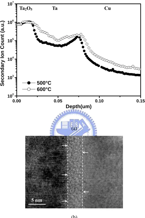
Figure 2.2(a) illustrates the SIMS depth profiles of the O elements in the Ta2O5/Ta/Cu/Ta sample following annealing at 500 and 600°C in oxygen ambient. The annealing was performed after the Ta2O5 film was deposited. Oxygen diffusion is found after annealing. The oxygen contents in Ta and Cu films increase with increasing annealing temperature. Oxygen atoms will diffuse along the grain boundaries of the Ta crystal and react with the Ta layer during annealing. The high-resolution TEM image in Fig. 2.2(b) clearly shows that an interlayer of thickness 4-5 nm is formed between Cu and Ta layers after annealing at 600°C in oxygen. Figure 2.3(a) displays the SIMS depth profiles of the O elements in the Ta2O5/Al/Ta/Cu/Ta sample after annealing at 500 and 600°C. Almost no indication exist that oxygen atoms diffuse into the Ta and Cu layer. The SIMS observation shown is consistent with the high-resolution TEM micrograph of Ta2O5/Al/Ta/Cu/Ta
structures (Fig. 2.3(b)) after annealing at 600°C in oxygen. No oxygen defection or reaction is observed between the Ta and Cu layers in the Ta2O5/Al/Ta/Cu/Ta samples. Significant improvement in thermal stability is obtained, compared with the samples without thin Al film, apparently owing to the barrier effectiveness of Al/Ta layers. However, the effective dielectric constant is about 18 instead of the value of 25 for pure Ta2O5. Figure 2.4 shows the TEM micrograph of the Cu/Ta/Ta2O5/Al/Ta/Cu device after thermal annealing at 600°C and reveals that the ultra thin film with an amorphous structure is formed between Ta2O5 and Al layers.
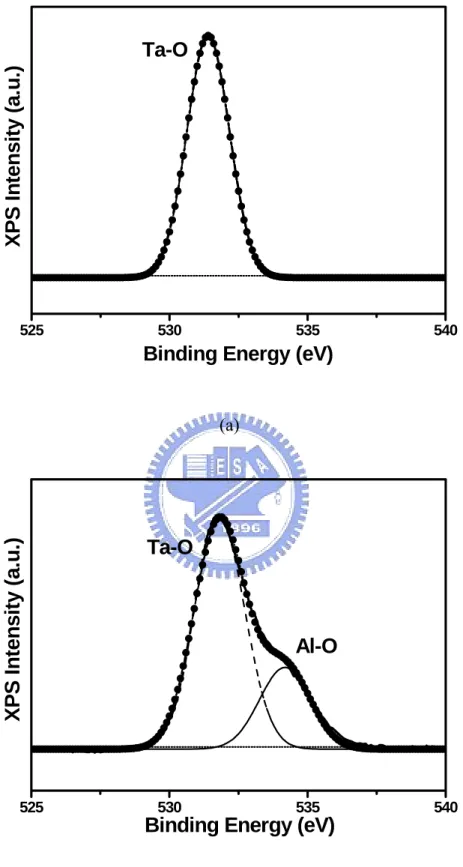
To identify this amorphous layer, the O 1s XPS spectra of Ta2O5 films deposited on Ta/Cu/Ta and Al/Ta/Cu/Ta electrodes were analyzed and are depicted in Fig. 2.5. Ta2O5 films were sputtered onto the electrodes for 5 min to form a layer of Ta2O5 of thickness ≤ 10 nm and then both samples were ion etched in order to expose the interfaces of the Ta2O5-Ta and Ta2O5-Al. The O 1s spectra presented in Fig. 2.5(a) show that the oxygen photoelectrons are in the Ta-O state. The standard O 1s peak position is located at ~531 eV. The O 1s spectra presented in Fig. 2.5(b) show that the oxygen photoelectrons are in the Ta-O and Al-O states, indicating formation of an Al2O3 layer [45]. In fact, formation of a dense monolayer of Al2O3 layer results in self-protection to oxidation and stops further oxygen diffusion. The layer behaves as an effective diffusion barrier to protect the underlying Cu and Ta layers [46,47].The formation of Al2O3 is thermodynamically favorable compared to Cu oxide, due to the large difference in oxide formation energy between Al (-226 kcal/g mol O2) and Cu (-53 kcal/g mol O2). Therefore, the Al2O3 layer will behave as an effective diffusion barrier to protect the underlying Cu and Ta layers.
Figure 2.6 displays leakage current densities of Ta2O5 films deposited on Al/Ta/Cu/Ta bottom electrodes after annealing at various temperatures in O2 ambient. The thickness of the dielectric layer is the total thickness of the Ta2O5 and Al2O3 films. The leakage current density of the as-deposited Ta2O5 film is ~100 nA/cm2 and decreases to ~1 nA/cm2 at 1 MV/cm after annealing at 600°C due to elimination of oxygen vacancies and bond defects. Atanassova et al. have reported that oxygen annealing may affect the concentration of the oxygen vacancies and non perfect bonds in the initial layers and consequently leads to leakage current reduction [48]. Several post-deposition treatments were investigated and successfully applied to reduce the oxygen vacancies and improve the electrical properties of Ta2O5 thin film [7]. Electrical properties of Ta2O5 MIM capacitors with various bottom electrodes, including Cu/Ta, Ta/Cu/Ta, and Al/Ta/Cu/Ta, were further compared and investigated. Figure 2.7 displays the leakage current densities as a function of electrical field up to 6 MV/cm following annealing at 600°C for 30 min. The leakage current densities are ~250 and 1.2-1.5 nA/cm2 at 1 MV/cm for Cu/Ta and Ta/Cu/Ta bottom electrodes. The lowest leakage current density of 1 nA/cm2 is measured for the Al/Ta/Cu/Ta bottom electrode. Also, the leakage current densities of Ta2O5 MIM capacitors with Al/Ta/Cu/Ta bottom electrodes are much lower than those reported by Ezhivalavan and Tseng [22,49]. The breakdown field (Ebd) for the Al/Ta/Cu/Ta bottom electrode is approximately 5.2 MV/cm (at 10-6 A/cm2) and higher than those for the Cu/Ta and Ta/Cu/Ta bottom electrodes of around 1.4 and 3.7 MV/cm.
2.3.1-3 Electrical Mechanism
Leakage current is a key parameter for ultra large scale integrated circuit applications. The leakage current in the Ta2O5 MIM capacitor may be due to several
mechanisms, including Schottky emission, Poole-Frenkel effect, electronic hopping conduction and tunneling [7,48,50-54]. The leakage current density versus electric field (J-E) characteristics of MIM capacitor using bottom and top electrodes of different work function will be highly asymmetric with the voltage polarity for the Schottky emission and symmetric for the Poole-Frenkel emission [55]. In this study, symmetric J-E characteristics were observed for Ta2O5 MIM capacitors with Al/Ta/Cu/Ta bottom electrodes and Ta/Cu top electrodes. This behavior indicates that Poole-Frenkel emission is the possible dominant conduction mechanism for leakage currents. The Poole-Frenkel effect predicts a field-dependent behavior of the form
⎟ ⎠ ⎞ ⎜ ⎝ ⎛ ⎟ ⎠ ⎞ ⎜ ⎝ ⎛− = 0 PF E1 2 kT kT q CE J exp φ exp β / (2.1)
where J denotes current density, T denotes the absolute temperature, q is the electronic charge, φ0 is the barrier height, krepresents the Boltzmann constant, E represents electric field, C is a constant and β is defined by
2 / 1 0 3 ⎟⎟ ⎠ ⎞ ⎜⎜ ⎝ ⎛ = ε πε βPF q (2.2)
where ε0 is the permittivity of free space and ε denotes the high-frequency dielectric constant. Poole-Frenkel conduction is due to field-enhanced thermal excitation of trapped electrons in the insulator into the conduction band. Figure 2.8(a) shows the logarithmic current density divided by the electric field as a function of the square root of the electric field [ln(J/E) vs. E1/2]. A good linearity is observed for the field E > 1.5 MV/cm for the plots. Furthermore, the dielectric constant deduced from the slope of the linear region of the Poole-Frenkel emission graph yields an ε value 9.21 almost equal to the measured. The results indicate that the conduction mechanism is dominated by Poole-Frenkel effect for the field E > 1.5 MV/cm. In the case of the Al/Ta/Cu/Ta bottom electrode, the temperature dependence of J-E
characteristics of the Ta2O5 capacitors was further studied. The leakage current increases exponentially with the temperature, as shown in Figs. 2.8(b) and (c). These results reveal that it is affected by trap charge density and the behavior shown in these plots indicates the Poole-Frenkel mechanism.
Figures 2.9(a) and (b) illustrate conduction mechanisms of Ta2O5 MIM capacitors with Ta/Cu/Ta and Al/Ta/Cu/Ta bottom electrodes. Some activated oxygen in the Ta2O5 film could diffuse into the Ta/Cu/Ta bottom electrode and react with the Ta layer during annealing. The oxygen vacancy acts as an electron trap with certain trap level in the energy band diagram. The traps act as stepping sites for electrons and facilitate their transport through the oxide. Moreover, the barrier height becomes low when the oxygen vacancies accumulate at the interface of the Ta2O5-metal electrode [56]. Ta/Cu/Ta bottom electrodes could result in more oxygen vacancies at the Ta2O5-Ta interface compared to Al/Ta/Cu/Ta bottom electrodes. When the top electrode is positively biased, electrons are relatively easily injected from the Ta/Cu/Ta bottom electrode into the tantalum oxide layer and further conductivity is governed by Poole-Frenkel effect (Fig. 2.9(a)). An interfacial Al2O3 layer is formed at the Ta2O5-Al interface for the Al/Ta/Cu/Ta bottom electrode. The formation of this layer can lead to modification of the conduction mechanism due to the difference in the band gaps of Ta2O5 and Al2O3. Ta2O5 and Al2O3 have band gaps of 4.4 and 8.8 eV, respectively [57]. It is found that the dominant conduction mechanism is also Poole-Frenkel effect for the Al/Ta/Cu/Ta bottom electrode from analyses of J-E characteristics. However, the interfacial Al2O3 layer will result in self-protection to oxidation and stop further oxygen diffusion. Reduction of oxygen vacancies leads to decreasing trap site, and leakage currents of Ta2O5 MIM capacitors with Al/Ta/Cu/Ta bottom electrodes could be reduced.
2.3.1-4 Device Lifetime
Nowadays, the time-dependent dielectric breakdown (TDDB) is an important reliability indicator of the MIM capacitor. Figure 2.10 illustrates cumulative probabilities of breakdown fields for Ta2O5 MIM capacitors with various bottom electrodes. Breakdown is defined as occurring when the leakage current density increases to 10-6 A/cm2. Obviously, the Cu/Ta/Ta2O5/Al/Ta/Cu/Ta MIM capacitors exhibit better breakdown behaviors than Cu/Ta/Ta2O5/Ta/Cu/Ta and Cu/Ta/Ta2O5/Cu/Ta MIM capacitors. Figure 2.11 shows the TDDB lifetime as a function of electric field for Ta2O5 MIM capacitors with various bottom electrodes. The Ta2O5 MIM capacitors with Al/Ta/Cu/Ta bottom electrodes have a longer lifetime than the others. The extrapolated long-term lifetime indicates that the Ta2O5 MIM capacitors with the Al/Ta/Cu/Ta bottom electrodes can survive ten years at a stress field of 1.2 MV/cm. Moreover, the plotted points follow straight lines and random failure modes are not observed, indicating the Ta2O5 MIM capacitors with the Cu-based bottom electrodes are of high quality and good uniformity.
2.3.2 Ta
2O
5MIM Capacitor using Low-temperature ICP-N
2O Plasma
2.3.2-1 Electrical Characteristic
Figure 2.12 presents the leakage current densities of the reference, F-O2, PE-N2O and ICP-N2O samples as a function of electric field up to ±4.5 MV/cm. Asymmetric current density vs. electric field (J-E) curves are observed. After post treatments, the leakage current is more decreased at a negative bias than at a positive bias. The leakage current at negative bias is influenced primarily by the interface of the Ta2O5 and Ta top electrode. The lowest leakage current densities were measured on the ICP-N2O sample, yielding a value of 4.0×10⁻¹⁰ A/cm2 at an electric field of -1 MV/cm, which is less than 3.8×10⁻⁹ A/cm2 for the PE-N
2O sample, 3.8×10⁻⁷ A/cm2 for the reference, and 5.7×10⁻⁸ A/cm2 for the F-O
2 sample. Also, the leakage current density of the ICP-N2O sample was lower than that in ref. [49] at an electric field of 1 MV/cm. After the Ta2O5 films were deposited, the oxygen escaped and oxygen vacancies were formed, according to,
2 '' 2 1 2e O V Oo←⎯→ o + −+ (2.3) where Oo, V and eo''
- represent the oxygen ion in its normal state, an oxygen
vacancy and an electron, respectively. A high concentration of oxygen vacancies caused electrons to be generated and a large leakage current to flow. Treatment with oxygen-containing plasma yielded active oxygen atoms and reduced oxygen vacancies, and ultimately improved the quality of Ta2O5 films.
Figure 2.12 indicates that ICP-N2O and PE-N2O samples have better electrical characteristics than the F-O2 sample. Many studies presented similar results, and have established that the nitridation and oxidation are controlled by the mobility of
nitrogen- and oxygen-based adatoms during the N2O plasma treatment [58-62]. N2O is a stronger oxidizing agent than O2 because free O atoms are more easily produced according to the reaction [63,64],
O O2 →2 (2.4) − −+N O→NO+N +e e 2 (2.5) O N NO N + → 2+ (2.6)
The activation energy in Eq. (2) is 5.12 eV, whereas that in Eqs. (3) and (4) is 2.51 eV. This result can be easily explained by the fact that less energy is required to break the N-O bond in a N2O molecule than the O=O bond in an O2 molecule. The excited oxygen atoms diffused rapidly into the Ta2O5 films and reduced the degree of imperfection and the concentration of oxygen vacancy. In addition, atomic N and surface-generated ions (NO) have been implicated in the nitridation process.
2.3.2-2 Physical Characteristics
Figure 2.13 illustrates the SIMS depth profiles of the O elements in the F-O2 and ICP-N2O samples. The apparent oxygen diffusion is found in F-O2 sample due to the oxygen atoms diffuse along the grain boundaries of the Ta crystal and react with the Ta layer during annealing. Nevertheless, almost no indication exists that oxygen atoms diffuse into the Ta layer in ICP-N2O sample due to low-temperature plasma treatment.
The leakage current density in the ICP-N2O sample is much lower than that in the PE-N2O sample at a negative bias, as displayed in Fig. 2.12. The influence of N2O plasma on Ta2O5 layer increases the concentration of oxygen atoms (or reduces the number of oxygen vacancies) in the Ta2O5 film. A PECVD system cannot generate high-density plasma. In fact, generating plasma even in a magnetic field at a chamber
pressure of only a few mtorr is very difficult [65]. In an ICP system, a flowing RF current in the coils easily generates a changing magnetic field, which in turn induces a
changing electric field through inductive coupling. Therefore, the inductively coupled electric field accelerates electrons at low pressure. The electronic mean free path may be shorter than the gap between the electrodes, so enough ionizing collisions occur. Hence, inductively coupled plasma reactors produce a high electron temperature that efficiently dissociates the N2O gas under pressure and causes more O radicals and ions to be present. Previous studies demonstrated that the oxidant produced under high-density plasma discharge is more reactive than the primary reactant used in plasma O2 annealing [66]. Accordingly, the high concentration of oxidants may explain why the leakage current density in the ICP-N2O sample is lower than that in the PE-N2O sample. Another reason may be the resulting roughness of the Ta2O5 layer. The Ta2O5 surfaces of the F-O2 and PE-N2O samples are clearly rougher than that of the ICP-N2O sample, as displayed in Fig. 2.14. It is believed the reactions or bombardments of energetic radicals and ions would occur during plasma treatment. They could sputter the films and make them smooth. The roughness effect can be interpreted as an image force that reduces the barrier height [11,67]. Table 2.3 summaries the electrical properties of Ta/Ta2O5/Ta capacitors with various post treatments. The breakdown field is defined as the electric field when leakage current density exceeds 10-6 A/cm2 under a positive bias. The breakdown fields of the reference and the F-O2 samples are approximately 1.2-1.9 MV/cm and that of the PE-N2O sample is 2.7 MV/cm. The excellent breakdown field of the ICP-N2O sample is 4.2 MV/cm. The improvement in breakdown field is attributed to the reduced surface roughness after treatments. A smooth surface can suppress the local accumulation of electrons and is responsible for the uniform electric field, and hence the ICP-N2O sample has a high breakdown field.
2.3.2-3 Plasma Treatment Mechanism
Figure 2.15 depicts the proposed schematic diagram of N2O plasma treatment on the Ta2O5 film based on the above results. Plasma treatment modifies the surface and causes ion bombardment effects. The principal dissociation products (N, O, and NO) of N2O would modify the surface of Ta2O5 films. The O atoms were accelerated toward the Ta2O5 film, where they were adsorbed and incorporated in oxygen vacancies. The dissociation of gas importantly affects the results of plasma treatment. The leakage current density of the ICP-N2O sample is one order of magnitude lower than that of the PE-N2O sample at an electric field of -1 MV/cm, because the concentration of oxygen vacancy is lower and effect of nitridation is higher following ICP than PE treatment.
2.3.2-4 Device Lifetime
Figure 2.16 shows the leakage current density versus time characteristics at high stress electric fields. At the beginning of the stress test, the leakage current fell rapidly. The decrease in the leakage current was believed to be caused by electron trapping [68-70]. The drop was gradual during the middle stage of the stress test. However, the leakage current rapidly increased and fatal breakdown occurred after the stress was applied for a longer period. Fatal breakdown is defined as leakage current density increases to 10-3 A/cm2 or ten times higher than the value at the previous one second time step. The data indicates that lower leakage films have longer breakdown lifetime. The ICP-N2O sample has a lower leakage current and longer breakdown lifetime under the stress at a constant electric field of 1.8 MV/cm. The leakage
currents in F-O2 and PE-N2O samples are higher and associated with a shorter time to breakdown at constant fields of 1.2 and 1.6 MV/cm, respectively. Breakdown is manifested by the formation of a conductive path through the oxide initiated by the presence of weak spots [48]. Local field enhancements at the weak spots cause vacancy-related breakdowns. The high-density local vacancies, including traps, are responsible for vacancy-related breakdown. Furthermore, TDDB lifetime was studied under various equivalent electric fields. The ICP-N2O sample exhibits a longer-term reliability than the PE-N2O, F-O2, and reference samples and the samples in ref. [49]. The extrapolated long-term lifetime demonstrates that the ICP-N2O sample can survive 10 years at a stress field of 1.61 MV/cm, as listed in Table 2.3.
2.3.2-5 Electrical Mechanism
The leakage current in the Ta/Ta2O5/Ta capacitor may be due to several mechanisms, including Schottky emission, Poole-Frenkel effect, electronic hopping conduction and tunneling [9,48,50-53]. The leakage current density versus electric field (J-E) characteristics of MIM capacitor will be highly asymmetric with the
voltage polarity for the Schottky emission. In this study, asymmetric J-E
characteristics were observed, as shown in Fig. 2.12. The Schottky current is due to electrons which transit above the potential barrier at the surface of a metal or semiconductor, and is typical of the electrode-limited current. A current density-electric field relation for Schottky emission is given by the following equation [9,50]. ⎟ ⎠ ⎞ ⎜ ⎝ ⎛ ⎟ ⎠ ⎞ ⎜ ⎝ ⎛− = 2exp 0 exp E1/2 kT kT q AT J φ β (2.7)
q is the electronic charge; φ0 is the barrier height; krepresents the Boltzmann constant; E represents the electric field, and β is defined as
2 / 1 0 3 4 ⎟⎟⎠ ⎞ ⎜⎜ ⎝ ⎛ = ε πε β q (2.8)
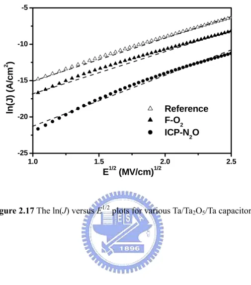
Where ε0 is the permittivity of free space and ε represents the high-frequency dielectric constant. Figure 2.17 shows the logarithmic current density as a function of the square root of the electric field [log(J) vs. E1/2]. A good linearity is observed for the plots, indicating that the Schottky emission is the possible dominant conduction mechanism for leakage currents, whereby electrons from the cathode overcome the Ta/Ta2O5 energy barrier before being emitted into the Ta2O5. The Schottky emission can be explained when an electron enters the dielectric, it produces an image field that adds and lowers the barrier field, resulting in a reduced barrier height and an enhanced current given.
Figures 2.18(a) and (b) illustrate conduction mechanisms of Ta/Cu/Ta capacitors with O2 furnace annealing and inductively coupled N2O plasma post-treatments, respectively. The Schottky emission is the possible dominant conduction mechanism for leakage currents. Surface roughness and oxygen vacancy are attributed to resulting conduction mechanism in the study. The F-O2 sample has a rougher surface than the ICP-N2O sample, as shown in Fig. 2.14. It was reported that surface roughness yields on the image potential were as high as high as even 10%-60% compared to that of a flat interface [11]. Some activated oxygen in the Ta2O5 film could diffuse into and react with the Ta bottom electrode layer during annealing. The oxygen vacancy acts as an electron trap with certain trap level in the energy band diagram. The traps act as stepping sites for electrons and facilitate their transport through the oxide. A thin highly oxygen-deficient layer remains in the tantalum oxide film adjacent to the Ta electrode for the F-O2 sample, as shown in
SIMS analyses of Fig. 2.13. The barrier height becomes low when the oxygen vacancies accumulate at the interface of the Ta2O5-metal electrode [37,56]. The F-O2 sample has a higher interfacial barrier compared to the ICP-N2O sample due to higher surface roughness and oxygen vacancy concentration, as shown in Fig. 2.18. When the top electrode is negatively biased, electrons are relatively easily injected from the Ta top electrode into the tantalum oxide layer and further conductivity is governed via trap sites.
2.4 Summary
Multilayered Al/Ta/Cu/Ta electrodes enhance the properties of the Ta2O5 MIM capacitors with Cu-based electrodes. This work found that the capacitors demonstrated a significant improving capability against oxygen diffusion after inserting an Al film. This improvement is attributed to a dense Al2O3 film formed on the surface of the Al/Ta/Cu/Ta bottom electrode after thermal annealing in oxygen ambient. Ultra-low leakage current density (1 nA/cm2 at 1 MV/cm) and high breakdown field (5.2 MV/cm at 10-6 A/cm2) are obtained for Ta2O5 MIM capacitors with Al/Ta/Cu/Ta electrodes because of reducing oxygen vacancy in tantalum oxide films. Ta2O5 MIM capacitors with Al/Ta/Cu/Ta electrodes also show less charge trapping and better TDDB properties. Al/Ta/Cu/Ta electrodes enable the integration of Cu electrodes with high-dielectric constant tantalum oxide thin films for high-frequency devices at interconnect levels.
The electrical properties of Ta2O5 thin films with MIM structures following the inductively coupled N2O plasma (ICP-N2O) post treatments were examined. The resulting Ta/Ta2O5/Ta capacitors have low leakage current densities (4.0×10⁻¹⁰ A/cm2 under 1 MV/cm), high breakdown fields (4.2 MV/cm at 10-6 A/cm2), and lifetimes of over 10 years at 1.61 MV/cm due to effectively dissociated N2O gas and reduced bombardment. The leakage current of the Ta/Ta2O5/Ta capacitor is dominated by Schottky emission. Oxygen vacancy and surface roughness are attributed to resulting conduction mechanism in the study. The low-temperature ICP system reduces the diffusion of oxygen atoms into the Ta bottom electrode, and lessens to the oxygen vacancies, while, the reactions of energetic radicals and ions reduce surface roughness. Consequently, the electrical characteristics and reliability of Ta/Ta2O5/Ta capacitors are enhanced after the low-temperature ICP treatments.
References
[1] J. A. Babcock, S. G. Balster, A. Pinto, C. Dirnecker, P. Steinmann, R. Jumpertz and B. El-Kareh, IEEE Electron Device Lett., 22, 230 ( 2001).
[2] M. Armacost, A. Augustin, P. Felsner, Y. Feng, G. Friese, J. Heidenreich, G. Hueckel, O. Prigge and K. Stein, in Int. Electron Devices Meeting Tech. Dig.,
157 (2000).
[3] A. Kar-Roy, C. Hu, M. Racanelli, C. A. Compton, P. Kempf, G. Jolly, P. N. Sherman, J. Zheng, Z. Zhang and A. Yin, in Proc. IITC, 245 (1999).
[4] S. J. Ding, C. Zhu and M. F. Li and D. W. Zhang, Appl. Phys. Lett. 87, 053501
(2005).
[5] H. Hu, C. Zhu, X. Yu, A. Chin, M. F. Li, B. J. Cho, D. L. Kwong, P. D. Foo, M.
B. Yu, X. Liu and J. Winkler, IEEE Electron Device Lett., 24(2), 60 (2003).
[6] R. B. van Dover, R. M. Fleming, R. M. Schneemeyer, G. B. Alers and D. J. Werder, in Int. Electron Devices Meeting Tech. Dig., 823 (1998).
[7] C. H. Ng, C. S. Ho, S. F. S. Chu and S. C. Sun, IEEE Trans. Electron Devices
52(7), 1399 (2005).
[8] W. D. Kim, J. H. Joo, Y. K. Jeong, S. J. Won, S. Y. Park, S. C. Lee, C. Y. Yoo, S. T. Kim and J. T. Moon, in IEDM Tech. Dig., 263 (2001).
[9] C. Chaneliere, J. L. Autran, R. A. B. Devine and B. Balland, Mater. Sci. Eng., R22, 269 (1998).
[10] M. Hiratani, S. Kimura, T. Hamada, S. Iijima and N. Nakanishi, Appl. Phys. Lett., 81(13), 2433 (2002).
[11] Y. S. Kim, Y. H. Lee, K. M. Lim and M. Y. Sung, Appl. Phys. Lett., 74(19),
2800 (1999).
[12] J. P. Chang, M. L. Steigerwald, R. M. Fleming, R. L. Opila and G. B. Alers,
[13] R. M. Fleming, D. V. Lang, C. D. W. Jones, M. L. Steigerwald, D. W. Murphy, G. B. Alers, Y.-H. Wong, R. B. van Dover, J. R. Kwo and A. M. Sergent, J. Appl. Phys., 88(2), 850 (2000).
[14] K. M. A. Salam, H. Fukuda and S. Nomura, J. Appl. Phys., 93(2), 1169 (2003).
[15] Z. W. Fu, F. Huang, Y. Q. Chu, Y. Zhang and Q. Z. Qin, J. Electrochem. Soc., 150(6), A776 (2003).
[16] S. Ezhilvalavan and T. Y. Tseng, J. Appl. Phys., 83, 4797 (1998).
[17] J. W. Lee, H. S. Song, K. M. Kim, J. M. Lee and J. S. Roh, J. Electrochem. Soc., 149(6), F56 (2002).
[18] C. S. Liangz and J. M. Wu, J. Electrochem. Soc., 152(12), F213 (2005).
[19] N. Cramer, A. Mahmud and T. S. Kalkur, Appl. Phys. Lett. 87, 032903 (2005).
[20] M. C. Chiu, C. F. Cheng, W. T. Wu and F. S. Shieu, J. Electrochem. Soc., 152(6), F66 (2005).
[21] J. H. Joo, J. M. Seon, Y. C. Jeon, K. Y. Oh, J. S. Roh and J. J. Kim, Appl. Phys. Lett., 70, 3053 (1997).
[22] S. Ezhilvalavan and T. Y. Tseng, Thin Solid Films, 360, 268 (2000).
[23] W. Fan, S. Saha, J. A. Carlisle, O. Auciello, R. P. H. Chang and R. Ramesh, Appl. Phys. Lett., 82(9), 1452 (2003).
[24] W. L. Yang, W. F. Wu, D. G. Liu, C. C. Wu and K. L. Ou, Solid-State Electron., 45, 149-158 (2001).
[25] W. F. Wu, K. L. Ou, C. P. Chou and C. C. Wu, J. Electrochem. Soc., 150, G83
(2003).
[26] K. L. Ou, W. F. Wu, C. P. Chou, S. Y. Chiou and C. C. Wu, J. Vac. Sci. Technol. B 20(5), 2154 (2002).
[27] K. L. Ou, M. H. Lin and S. Y. Chiou, Electrochemical and Solid-State Letters, 7(11), G272 (2004).
[28] K. W. Kwon, H. J. Lee and R. Sinclair, Appl. Phys. Lett., 75(7), 935 (1999).
[29] J. C. Lin and C. Lee, J. Electrochem. Soc., 146(9), G3466 (1999).
[30] T. P. Liu, W.P. Huang and T.B. Wu, IEEE Trans. Electron. Devices, 50, 1425
(2003).
[31] J. W. Kim, S. D. Nam, S. H. Lee, S. J. Won, W. D. Kim, C. Y. Yoo, Y. W. Park, S. I. Lee and M. Y. Lee, in IEDM Technical Digest. International, 793 (1999).
[32] J. Y. Tewg, Y. Kuo, J. Lu and B. W. Schueler, J. Electrochem. Soc., 151(3), F59
(2004).
[33] W. D. Kim, J. H. Joo, Y. K. Jeong, S. J. Won, S. Y. Park, S. C. Lee, C. Y. Yoo, S. T. Kim and J. T. Moon, in IEDM Technical Digest. International, 263 (2001).
[34] F. C. Chiu, J. J. Wang, J. Y. m. Lee and S. C. Wu, J. Appl. Phys. 81(10), 6911
(1997).
[35] K. S. Ahn and Y. E. Sung, J. Vac. Sci. Technol. A., 19(6), 2840 (2001).
[36] J. H. Huang, Y. S. Lai and J. S. Chen, J. Electrochem. Soc., 148(7), F133
(2001).
[37] K. C. Tsai, W. F. Wu, C. G. Chao and C. P. Kuan, J. Electrochem. Soc., in press,
(2006).
[38] T. Aoyama, S. Saida, Y. Okayama, M. Fujisaki, K. Imai and T. Arikado, J. Electrochem. Soc., 143, 977 (1996).
[39] E. Atanassova and A. Paskaleva, Microelectronics Reliability, 42, 157 (2002).
[40] C. Chaneliere, S. Four, J. L. Autran and R. A. B. Devine, Electrochem. Solid-State Lett., 2(6), 291 (1999).
[41] W. R. Hitchens, W. C. Krusell and D. M. Dobkin, J. Electrochem. Soc., 140,
2615 (1993).
[42] J. M. Shieh, K. C. Tsai and B. T. Dai, Appl. Phys. Lett., 81, 1294 (2002).
(2003).
[44] J. M. Shieh, K. C. Tsai and B. T. Dai, Appl. Phys. Lett., 82, 1914 (2003).
[45] J. F. Moulder, W. F. Stickle, P. E. Sobol and K. D. Bomben, Handbook of X-ray Photoelectron Spectroscopy, Physical Electronics, Eden Prairie, MN, 44 (1995).
[46] W. A. Lanford, P. J. Ding, W. Wang, S. Hymes and S. P. Muraka, Thin Solid Films, 262, 234 (1995).
[47] W. A. Lanford, S. Bedell, P. Isberg, Hjovarsson, S. K. Lakshmanan and W. N. Gill, J. Appl. Phys., 85, 1487 (1999).
[48] E. Atanassova, N. Novkovski, A. Paskaleva and M. P- Gjorgjevich, Solid-State Elec., 46, 1887 (2002).
[49] S. Ezhilvalavan and T. Y. Tseng, in proc. Electronic Components and Technology Conference, 1042 (1999).
[50] S. M. Sze, Physics of Semiconductor Device, Wiley, New York, 478 (1981).
[51] C. Chaneliere, J. L. Autran and R. A. B. Devine, J. Appl. Phys., 86, 480 (1999).
[52] D. E. Kotecki et al. IBM J. Res. Develop. 43(3), 367 (1999).
[53] T. Hara, IEEE Trans. Device Mater. Rrliability, 4(2), 268 (2004).
[54] Y. B. Lin and J. Y. m. Lee, J. Appl. Phys., 87(4), 1841 (2000).
[55] C. S. Chang, T. P. Liu and T. B. Wu, J. Appl. Phys., 88, 7242 (2000).
[56] J. H. Joo, Y. C. Jeon, J. M. Seon, K. Y. Oh, J. S. Roh and J. J. Kim, Jpn. J. Appl. Phys., 36, 4382 (1997).
[57] J. Robertson, Appl. Surf. Sci., 190, 2 (2002).
[58] S. C. Sun and T. F. Chen, IEEE Electron Device Lett., EDL-17, 355 (1996).
[59] K. C. Tsai, W. F. Wu, J. C. Chen, C. G. Chao and T. J. Pan, J. Electrochem. Soc. 152(1), G83-G91 (2005).
[60] K. C. Tsai, W. F. Wu, J. C. Chen, C. G. Chao and T. J. Pan, J. Vac. Sci. Technol.