國 立 交 通 大 學
光電工程學系暨顯示科技研究所
碩 士 論 文
具輕摻雜汲極結構之多晶矽薄膜電晶體
之溫度效應研究
Study on Temperature Response of Poly-Si TFT’s
with LDD Structure
研 究 生:王光明
指導教授:冉曉雯 博士
具輕摻雜汲極結構之多晶矽薄膜電晶體之溫度效應研究
Study on Temperature Response of Poly-Si TFT’s with LDD Structure
研 究 生:王光明 Student:Kuang-Ming Wang
指導教授:冉曉雯 博士 Advisor : Dr. Hsiao-Wen Zan
國 立 交 通 大 學
光電工程學系暨顯示科技研究所
碩 士 論 文
A Thesis
Submitted to Department of Photonics and Institute of Display
College of Electrical and Computer Engineering
National Chiao-Tung University
In Partial Fulfillment of the Requirements
For the Degree of
Master
in
Electro-Optical Engineering
September 2007
Hsinchu, Taiwan
中 華 民 國 九 十 六 年 九 月
具輕摻雜汲極結構之多晶矽薄膜電晶體之溫度效應研究
研究生:王光明 指導教授:冉曉雯 博士
國立交通大學
光電工程學系暨顯示科技研究所
摘 要
多晶矽薄膜電晶體在面板技術的應用上,由於具有高遷移率,有機會整合面板周邊 電路,實現系統面板(System on Panel)的目標。而在實際的應用上,多晶矽薄膜電晶 體通常會使用輕摻雜汲極結構。在本論文中,我們將分別針對多晶矽薄膜電晶體的載子 遷移率,以及輕摻雜汲極區域所造成的寄生電阻效應,做相關的實驗分析與研究,尤其 著重於遷移率與寄生電阻的溫度效應。 首先,我們提出一個遷移率模型,此模型是以熱電子發射效應以及聲子散射效應交 互作用後所產生之溫度效應作為理論基礎來建構。我們利用該遷移率模型,針對無輕摻 雜汲極結構的元件進行載子遷移率的模擬。而不論是在遷移率的模擬或是在元件電流特 性的模擬中,都可以在不同的閘極偏壓與不同的環境溫度之下,分別得到與遷移率萃取 值以及元件電流測量值相當吻合的結果。 接下來,我們討論了輕摻雜汲極結構所造成的寄生電阻效應。針對具輕摻雜汲極結 構的元件,我們先由其電流特性計算出元件電阻,再以無輕摻雜汲極結構元件的電阻作 為參考電阻,將其電阻相減,即可得到輕摻雜汲極區域所造成的寄生電阻。而根據由此 萃取出的寄生電阻結果,我們發現寄生電阻會受到閘極偏壓的調變,而且對越短的輕摻 雜汲極長度而言,其寄生電阻受到閘極偏壓調變的情形會越嚴重。接著,我們利用 Silvaco 元件模擬軟體,針對具輕摻雜汲極的元件結構進行元件模 擬的工作。根據元件模擬的結果,可以推論出在閘極電極的周圍,存在一個寄生電晶體, 並且在溫度效應上,同樣受到熱電子發射效應的影響。此外,在距離閘極電極較遠的輕 摻雜汲極區域,並不受到閘極偏壓的調變,因此在同一溫度下可視為定電阻,而在合理 的推論下,我們認為此段未受閘極偏壓調變之輕摻雜汲極區域電阻,其溫度效應是由雜 質散射效應所主導。 最後,我們根據上述的假設與分析,針對具輕摻雜汲極結構的元件,提出了一個包 含溫度效應的寄生電阻模型,並且利用此寄生電阻模型,針對具輕摻雜汲極結構的元件 進行寄生電阻的模擬。而不論是在寄生電阻的模擬或是在元件電流特性的模擬中,都可 以在不同的閘極偏壓與不同的環境溫度之下,分別得到與寄生電阻萃取值以及元件電流 測量值相當吻合的結果。
Study on Temperature Response of Poly-Si TFT’s with LDD Structure
Student: Kuang-Ming Wang Advisor: Dr. Hsiao-Wen Zan
Department of Photonics and Institute of Display
National Chiao Tung University
Abstract
Polycrystalline silicon thin film transistors (Poly-Si TFT’s) have been studied extensively for their application on system-on-panel (SOP) technology due to the high mobility. For actual applications, lightly-doped drain (LDD) structure is usually applied to Poly-Si TFT’s. In this thesis, we will study on the effect of field effect mobility and parasitic resistance caused by LDD structure in Poly-Si TFT’s, especially on the temperature response of field effect mobility and parasitic resistance.
First, the mobility modeling of the Poly-Si TFT without LDD structure is performed by using the proposed mobility model. The proposed mobility model has taken thermionic emission effect and phonon scattering effect into account to explain the temperature response of field effect mobility. Excellent agreement between experimental and modeling results over the wide range of gate voltage and temperature is both obtained in the field effect mobility modeling and the transfer characteristics modeling by using the proposed mobility model for the Poly-Si TFT without LDD structure.
Next, the parasitic resistance effect due to LDD structure is discussed. The parasitic resistance caused by LDD structure is calculated by subtracting the device resistance of the Poly-Si TFT without LDD structure from the device resistance of the Poly-Si TFT’s with
LDD structure. According to the extracted parasitic resistance data, it is found that the parasitic resistance is modulated by gate bias and the modulation is more serious for the Poly-Si TFT’s with shorter LDD lengths.
After that, the device simulation results which are performed by Silvaco TCAD for the device with LDD structure show that parasitic transistor effect exists alongside the gate electrode. The parasitic transistor is also dominated by thermionic emission effect in temperature response. Besides, the resistance is treated as a pure resistor with a constant resistance at some temperature for the LDD region without gate bias modulation, and the mechanism of the temperature response in this series resistance region is preferred to conceive as impurity scattering effect.
Finally, the proposed parasitic resistance model is established basing on the analysis and the assumptions mentioned above. Good agreement between experimental and modeling results over the wide range of gate voltage and temperature is both obtained in the parasitic resistance modeling and the transfer characteristics modeling by using the proposed parasitic resistance model for the Poly-Si TFT’s with LDD structure.
誌 謝
兩年的碩士班生涯在轉眼間過去了,連同四年的大學生活在內,已經在交通大學度 過了六個寒暑。在交大的求學生涯裡,得到了許多人的支持與幫助,但要說到最感謝的 人,自然是從我身為大三的專題生開始到現在,一直在生活、學業與研究上給予我指導 與建議的指導教授,冉曉雯博士,曉雯老師。由於老師不遺餘力的教導,讓我累積了基 本的能力來從事研究;因為老師的帶領,讓我找到了適合自己的研究領域;與老師不定 時的討論,讓我在研究工作遇到瓶頸時能有所突破;在碩士論文的研究與寫作過程中, 老師更是我最大的助力與依靠。而老師在我碩士班的求學階段完成了終身大事,讓我也 有幸能沾沾喜氣,祝福老師在婚姻生活與研究工作上都能幸福快樂,謝謝老師! 其次,在進行實驗的過程中,要感謝曾一起工作的同事:陳信立經理、兆仟學長、 貞儀學姐、佳卉、振洲,感謝你們協助我完成量測實驗,而且除了幫忙進行元件的製造 之外,也在元件特性的分析上,給予我十分受用的建議。 此外,要感謝實驗室的博士班學長:國錫學長、士欽學長、政偉學長,你們的博學 讓我在課業或研究上有疑惑時,能夠很快地獲得幫助;尤其感謝國錫學長,謝謝你在我 投稿IDMC 論文時,所給予我的大力協助。還有感謝同屆的夥伴:而康、德倫、廷遠、 皇維、睿志、文馨、芸嘉,因為有你們的陪伴,共同奮鬥、一起歡笑、互相激勵,讓我 更有力量走到最後;尤其是從大一就和我結緣的而康,真的十分感激你多年來的陪伴與 支持。謝謝學弟妹們,你們讓實驗室就像個大家庭,也讓實驗室更加地溫暖。 最後,更要深深地感謝我的我的父母,謝謝你們從小到大對我的教誨,謝謝你們給 我如此自由的成長環境。如今我能略有小成,都是因為你們在背後的鼓勵與支持。還要 感謝我的女友,子瑜,謝謝妳總是在我感到落寞時給我鼓勵與信心!這本論文的完成, 是我成長的一個紀錄。僅以這篇論文,獻給我的老師、家人與好友。 光明 2007 初秋 于新竹交通大學Contents
Chinese Abstract I
English Abstract III
Acknowledgment
V
Contents VI
Table Captions VIII
Figure Captions X
Chapter 1 Introduction 1
1.1 An Overview of the Poly-Si TFT Technology 1
1.2 Mobility Models for Poly-Si TFT’s . 2
1.3 Motivation 3
1.4 Thesis Outline 4
Chapter 2 Modeling of the Poly-Si TFT’s without LDD Structure 6
2.1 Device Fabrication Process and Measurement Conditions 6
2.2 Modeling of Field Effect Mobility 7
2.2.1 The Proposed Mobility Model for Poly-Si TFT’s 7
2.2.2 Mobility Extraction Method 8
2.2.3 Mobility Modeling Results 9
2.3 Modeling of Transfer Characteristics 10
Chapter 3 Modeling of the Poly-Si TFT’s with LDD Structure 11
3.1.1 Parasitic Resistance under Various LDD Lengths 11
3.1.2 Device Simulation Results 12
3.2 Modeling of Parasitic Resistance 13
3.2.1 The Parasitic Resistance Model for Poly-Si TFT’s with LDD Structure 13 3.2.2 Parasitic Resistance Modeling Results 15
3.3 Modeling of Transfer Characteristics 17
Chapter 4 Conclusion 18
Appendix The Proposed Mobility Model for Poly-Si TFT’s 20
References 24
Tables 26
Table Captions
Table I (P.26)
The model parameter values of the proposed mobility model for the W/L = 6μm / 6μm N-type Poly-Si TFT without LDD structure
Table II (P.27)
The model parameter values of the proposed parasitic resistance model for the W/L = 6μm / 6μm N-type Poly-Si TFT with 0.5μm LDD length
Table III (P.27)
The model parameter values of the proposed parasitic resistance model for the W/L = 6μm / 6μm N-type Poly-Si TFT with 1.0μm LDD length
Table IV (P.28)
The model parameter values of the proposed parasitic resistance model for the W/L = 6μm / 6μm N-type Poly-Si TFT with 1.5μm LDD length
Table V (P.28)
The model parameter values of the proposed parasitic resistance model for the W/L = 6μm / 6μm N-type Poly-Si TFT with 2.0μm LDD length
Table VI (P.29)
The model parameter values of the proposed parasitic resistance model for the W/L = 6μm / 6μm N-type Poly-Si TFT with 3.0μm LDD length
Table VII (P.29)
The model parameter values of the proposed parasitic resistance model for the W/L = 6μm / 6μm N-type Poly-Si TFT with 3.5μm LDD length
Table VIII (P.30)
The model parameter values of the proposed parasitic resistance model for the W/L = 6μm / 30μm N-type Poly-Si TFT with 0.5μm LDD length
Table IX (P.30)
The model parameter values of the proposed parasitic resistance model for the W/L = 6μm / 30μm P-type Poly-Si TFT without LDD structure
Figure Captions
Chapter 2
Fig.2-1 The schematic cross-sectional view of the W/L = 6μm / 6μm N-type Poly-Si TFT with LDD structure (P.31)
Fig.2-2 The schematic cross-sectional view of the W/L = 6μm / 6μm N-type Poly-Si TFT’s without LDD structure (P.31)
Fig.2-3 The SEM image of the Poly-Si film annealed by ELA method under 420 mJ / cm2 laser energy (P.32)
Fig.2-4 The extraction method for the activation energy EA of the W/L = 6μm / 6μm N-type Poly-Si TFT without LDD structure due to thermionic emission effect (P.33) Fig.2-5 The activation energy EA extracted from the W/L = 6μm / 6μm N-type Poly-Si TFT
without LDD structure (P.33)
Fig.2-6 The comparison between the raw extracted mobility values and the modeling mobility values for the W/L = 6μm / 6μm N-type Poly-Si TFT without LDD
structure at various temperatures: (a) T = 253K, 298K and 348K; (b) T = 233K,
273K, 323K and 373K (P.34)
Fig.2-7 The comparison between the measured transfer characteristics and the modeling transfer characteristics for the W/L = 6μm / 6μm N-type Poly-Si TFT without LDD
structure at various temperatures: (a) T = 253K, 298K and 348K; (b) T = 233K,
273K, 323K and 373K (P.35)
Chapter 3
Fig.3-1 The parasitic resistance percentage comparison between the W/L = 6μm / 6μm N-type Poly-Si TFT’s with different LDD lengths from VGS=3V to VGS=15V
(P.36)
Fig.3-2 The relation between the parasitic resistance and the LDD length including the linear fits for the extracted data of the W/L = 6μm / 6μm N-type Poly-Si TFT’s with larger LDD lengths (P.36)
Fig.3-3 The device structure which is used in device simulation performed by Silvaco TCAD (P.37)
Fig.3-4 The comparison of the current density distribution simulation results between the devices (a) with and (b) without LDD structure (P.38)
Fig.3-5 The comparison of the zoom-in on current density distribution simulation results between the devices (a) with and (b) without LDD structure (P.39)
Fig.3-6 The comparison of the zoom-in on vertical electric field distribution simulation results between the devices (a) with and (b) without LDD structure (P.40)
Fig.3-7 The comparison of the current density distribution simulation results from source side (Distance = 0μm) to drain side (Distance = 20μm) between the devices (a) with and (b) without LDD structure (P.41)
Fig.3-8 The extraction method for the activation energy of the parasitic transistor EAN due to thermionic emission effect from the W/L = 6μm / 6μm N-type Poly-Si TFT with
0.5μm LDD length (P.42)
Fig.3-9 The activation energy of the parasitic transistor EAN extracted from the W/L = 6μm / 6μm N-type Poly-Si TFT with 0.5μm LDD length (P.42)
Fig.3-10 The comparison between the activation energy EA extracted from the measured transfer characteristics of the W/L = 6μm / 6μm N-type Poly-Si TFT without LDD
structure and the activation energy of the parasitic transistor EAN extracted from the extracted parasitic resistance of the W/L = 6μm / 6μm N-type Poly-Si TFT with
0.5μm LDD length (P.43)
scattering effect for the W/L = 6μm / 6μm N-type Poly-Si TFT with 3.5μm LDD
length (P.43)
Fig.3-12 The comparison between the extracted conductance and the modeling conductance for the W/L = 6μm / 6μm N-type Poly-Si TFT with 0.5μm LDD length at various temperatures: (a) T = 253K, 298K and 348K; (b) T = 233K, 273K, 323K and 373K (P.44)
Fig.3-13 The comparison between the extracted conductance and the modeling conductance for the W/L = 6μm / 6μm N-type Poly-Si TFT with 1.0μm LDD length at various temperatures: (a) T = 253K, 298K and 348K; (b) T = 233K, 273K, 323K and 373K (P.45)
Fig.3-14 The comparison between the extracted conductance and the modeling conductance for the W/L = 6μm / 6μm N-type Poly-Si TFT with 1.5μm LDD length at various temperatures: (a) T = 253K, 298K and 348K; (b) T = 233K, 273K, 323K and 373K (P.46)
Fig.3-15 The comparison between the extracted conductance and the modeling conductance for the W/L = 6μm / 6μm N-type Poly-Si TFT with 2.0μm LDD length at various temperatures: (a) T = 253K, 298K and 348K; (b) T = 233K, 273K, 323K and 373K (P.47)
Fig.3-16 The comparison between the extracted conductance and the modeling conductance for the W/L = 6μm / 6μm N-type Poly-Si TFT with 3.0μm LDD length at various temperatures: (a) T = 253K, 298K and 348K; (b) T = 233K, 273K, 323K and 373K (P.48)
Fig.3-17 The comparison between the extracted conductance and the modeling conductance for the W/L = 6μm / 6μm N-type Poly-Si TFT with 3.5μm LDD length at various temperatures: (a) T = 253K, 298K and 348K; (b) T = 233K, 273K, 323K and 373K (P.49)
Fig.3-18 The comparison between the measured transfer characteristics and the modeling transfer characteristics for the W/L = 6μm / 6μm N-type Poly-Si TFT with 0.5μm
LDD length at various temperatures: (a) T = 253K, 298K and 348K; (b) T = 233K,
273K, 323K and 373K (P.50)
Fig.3-19 The comparison between the measured transfer characteristics and the modeling transfer characteristics for the W/L = 6μm / 6μm N-type Poly-Si TFT with 1.0μm
LDD length at various temperatures: (a) T = 253K, 298K and 348K; (b) T = 233K,
273K, 323K and 373K (P.51)
Fig.3-20 The comparison between the measured transfer characteristics and the modeling transfer characteristics for the W/L = 6μm / 6μm N-type Poly-Si TFT with 1.5μm
LDD length at various temperatures: (a) T = 253K, 298K and 348K; (b) T = 233K,
273K, 323K and 373K (P.52)
Fig.3-21 The comparison between the measured transfer characteristics and the modeling transfer characteristics for the W/L = 6μm / 6μm N-type Poly-Si TFT with 2.0μm
LDD length at various temperatures: (a) T = 253K, 298K and 348K; (b) T = 233K,
273K, 323K and 373K (P.53)
Fig.3-22 The comparison between the measured transfer characteristics and the modeling transfer characteristics for the W/L = 6μm / 6μm N-type Poly-Si TFT with 3.0μm
LDD length at various temperatures: (a) T = 253K, 298K and 348K; (b) T = 233K,
273K, 323K and 373K (P.54)
Fig.3-23 The comparison between the measured transfer characteristics and the modeling transfer characteristics for the W/L = 6μm / 6μm N-type Poly-Si TFT with 3.5μm
LDD length at various temperatures: (a) T = 253K, 298K and 348K; (b) T = 233K,
Appendix
Fig.A-1 The illustration diagram of grain and grain boundary for the proposed mobility model (P.56)
Fig.A-2 The comparison between the raw extracted mobility values and the modeling mobility values for the W/L = 6μm / 30μm N-type Poly-Si TFT with 0.5μm LDD
length at various temperatures: (a) T = 253K, 298K and 348K; (b) T = 233K,
273K, 323K and 373K (P.57)
Fig.A-3 The comparison between the raw extracted mobility values and the modeling mobility values for the W/L = 6μm / 30μm P-type Poly-Si TFT without LDD
structure at various temperatures: (a) T = 253K, 298K and 348K; (b) T = 233K,
273K, 323K and 373K (P.58)
Fig.A-4 The temperature dependence of the model parameters including of the proposed mobility model (a) VT and (b)
μ
G / LGB for the W/L = 6μm / 30μm N-type Poly-Si TFT with 0.5μm LDD length (P.59)Fig.A-5 The temperature dependence of the model parameters including of the proposed mobility model (a) VT and (b)
μ
G / LGB for the W/L = 6μm / 30μm P-type Poly-Si TFT without LDD structure (P.60)Chapter 1
Introduction
1.1 An Overview of the Poly-Si TFT Technology
Polycrystalline silicon thin film transistors (Poly-Si TFT’s) have attracted more attention because of their wide applications on active matrix liquid crystal displays (AMLCD’s) [1-3], memory devices such as dynamic random access memories (DRAM’s) [4] and static random access memories (SRAM’s) [5], electrical programming read only memories (EPROM’s) [6] and electrical erasable programming read only memories (EEPROM’s) [7].
Unlike amorphous silicon (a-Si) TFT’s, Poly-Si TFT’s have much larger carrier mobility which usually exceeds 100 cm2 / V-sec by present mature technology. The superior carrier mobility is essential to successfully integrate Poly-Si TFT’s and peripheral driving circuits [5] on the same panel to reduce the assembly complexity and cost. Therefore, the low temperature process of Poly-Si TFT’s with high mobility makes it possible to realize the ultimate goal, system on panel (SOP) [8]. Furthermore, due to the higher mobility, the device dimension of Poly-Si TFT’s can be made smaller than that of a-Si TFT’s to get higher aperture ratio in each pixel and achieve high density and high resolution AMLCD’s.
However, there are still some problems existed in Poly-Si TFT’s. Comparing to single crystalline silicon (c-Si), Poly-Si has a lot of defects at grain boundaries. These defects, regarded as trap states, are located in the disordered grain boundary regions and degrade device performance severely. In other words, the performance of Poly-Si TFT’s is strongly affected by the grain structure inside the channel region. Thus, the larger grain with less grain boundary defects is desirable and currently many researches attempting to achieve this goal have been studied, such as solid phase crystallization (SPC) [9], metal induced lateral crystallization (MILC) [10] and laser crystallization [11]. Because the recrystallization
process will influence the quality of Poly-Si film, it will influence the device performance of Poly-Si TFT’s spontaneously. Thus, the device models should have the ability to be effectively applied to Poly-Si TFT’s fabricated from Poly-Si films of different film qualities. For example, the proposed mobility model which will be presented later in this thesis can be applied to Poly-Si TFT’s with different grain sizes by adjusting the model parameters, and the interactive influence between thermionic emission effect and phonon scattering effect is performed to express the temperature response.
1.2 Mobility Models for Poly-Si TFT’s
For Poly-Si TFT’s, unlike c-Si transistors, not all charges induced by gate voltage can become free carriers to contribute to drain current. Instead, one significant part of the gate-bias-induced charges will be captured by the trap states associated with grain boundaries. Therefore, field effect mobility will increase gradually with gate voltage because the ratio of free carrier density to induced charge density increases. This is so-called pseudo-subthreshold region which is caused by the decrease of energy barrier height at grain boundaries in Poly-Si TFT’s. M. Jacunski et al. had proposed an appropriate mobility model to take this effect into account empirically and the equation was expressed as: [12]
m th i t GS FET V V V η μ μ μ 2( ) 1 1 1 1 0 − + = (1-1)
where m,
μ
0 andμ
1 are extractable mobility parameters. But it is a pity that this model is not valid under various temperatures because the temperature effects such as phonon scattering effect at high gate biases are not under consideration. Thus, the above formula fails to precisely describe the behaviors of carrier mobility in Poly-Si TFT’s.To improve this problem, an empirical assumption with power law is applied to describe phonon scattering effect and to modify this mobility model, and the modified model equation
can be written as: m th i t GS FET V V V T T η μ μ μ β ) ( 2 1 1 1 1 0 0 − + ⎟⎟ ⎠ ⎞ ⎜⎜ ⎝ ⎛ = − (1-2)
where
β
stands for the temperature dependence due to phonon scattering effect.Besides, Apostolos T. Voutsas proposed another mobility model which was given as: [13]
GB Defect SIMOX app μ μ μ μ 1 1 1 1 = + + (1-3)
where
μ
app is the measured mobility,μ
SIMOX is the equivalent SIMOX mobility accounting for phonon scattering effect,μ
Defect is the mobility term attributed to intra-grain-defect scattering andμ
GB is the mobility term attributed to grain-boundary scattering, i.e. thermionic emission effect. However, this model is complicated to use because the fitting parameters are too many, or in other words, the parameter extraction procedure is too inextricable.In fact, we have proposed the mobility model basing on physical theories, and the proposed model is verified in different devices including N-type devices and P-type devices. The details and verification results of the proposed mobility model are described particularly in Appendix.
1.3 Motivation
The proposed mobility model (as shown in Appendix) is used to describe the electrical properties in device channel region. But for actual applications, lightly-doped drain (LDD) structure is usually applied to devices with total LDD length approaching 2μm or above. Therefore, LDD structure will influence the device performance more seriously with shorter channel length. The effect of LDD structure will be investigated in this thesis in detail, especially the temperature response of LDD structure.
TFT’s because LDD structure can effectively lower down drain electric field. The LDD region will produce an extra parasitic resistance and that will influence the performance of Poly-Si TFT’s considerably, but the modeling of parasitic resistance effect is not well-established so far.
When long channel devices are checked, parasitic resistance effect seems not so important because channel resistance is much larger and the difference caused by parasitic resistance can be eliminated by a global fitting in field effect mobility models. But for short channel devices, parasitic resistance effect becomes significant and the modeling of field effect mobility can not be achieved very well only by existing mobility models. The modeling of parasitic resistance effect due to LDD region should be taken into account in Poly-Si TFT device models and then the accurate modeling results of device electrical characteristics can be obtained. Therefore, the modeling of parasitic resistance effect is important to precisely predict the device performance of Poly-Si TFT’s with LDD structure, especially for the tendency toward short channel devices.
1.4 Thesis Outline
In Chapter 1, the various kinds of applications, the advantages and the disadvantages of Poly-Si TFT’s are introduced in a brief overview of the Poly-Si TFT technology. Then, several mobility models for Poly-Si TFT’s are discussed, and these models mainly emphasize on the effect of energy barrier height caused by grain boundary defects in Poly-Si TFT’s. Finally, the motivation of this work to study the parasitic resistance modeling of Poly-Si TFT’s with LDD structure is expressed.
In Chapter 2, the fabrication process and the measurement experimental conditions of the Poly-Si TFT’s used in this work are firstly described in brief. Following that, the proposed mobility model is presented and the physical basis of the proposed mobility model is also interpreted. The mobility extraction method from the measured data used in this work is
introduced and the extracted field effect mobility of the Ploy-Si TFT without LDD structure is then modeled over the wide range of gate voltage and temperature by the proposed mobility model. Besides, the measured transfer characteristics of the Poly-Si TFT without LDD structure are also simulated over the wide range of gate voltage and temperature basing on the field effect mobility fitting results of the proposed mobility model.
In Chapter 3, the parasitic resistance extraction method used in this work is introduced to extract the values of the parasitic resistance under different gate biases and several temperatures for the Poly-Si TFT’s with various LDD lengths. The dependence between the extracted parasitic resistance and the gate voltage is checked to discuss the possible mechanism. Next, the device simulation results including the current density distribution results and the vertical electric field distribution results performed by Silvaco TCAD are presented. Afterwards, the parasitic resistance model basing on the experimental results and the simulation results is proposed. The extracted parasitic resistance of the Poly-Si TFT’s with various LDD lengths is then modeled over the wide range of gate voltage and temperature by the proposed parasitic resistance model. Finally, the measured transfer characteristics of the Poly-Si TFT’s with various LDD lengths are also simulated over the wide range of gate voltage and temperature basing on the field effect mobility fitting results of the proposed mobility model from the Poly-Si TFT without LDD structure and the parasitic resistance fitting results of the proposed parasitic resistance model from the Poly-Si TFT’s with various LDD lengths.
In Chapter 4, the conclusions of the works done in this thesis are given.
In Appendix, the proposed mobility model is derived in detail and the physical basis is also interpreted particularly. In addition, the proposed model is verified in different devices including N-type devices and P-type devices and the analysis of the verification results are given.
Chapter 2
Modeling of the Poly-Si TFT’s without LDD Structure
2.1 Device Fabrication Process and Measurement Conditions
The typical top-gate, coplanar self-aligned Poly-Si TFT’s which were fabricated on the glass substrates and crystallized by excimer laser annealing (ELA) recrystallization technology are used in this study. The Poly-Si TFT’s with and without LDD structure were also fabricated, respectively. The schematic cross-sectional view of the devices with LDD structure is shown in Fig.2-1, and that of the devices without LDD structure is shown in Fig.2-2. The device fabrication process is described below.
First, the oxide buffer layer was deposited on the glass substrate to prevent the diffusion of the impurities existing in the glass substrate from the silicon layer. Then, the undoped 50-nm-thick a-Si layer was deposited on the buffer layer. After that, the a-Si films were recrystallized by ELA method with 420 mJ / cm2 laser energy, and the recrystallized Poly-Si films were patterned into the active islands. Afterward, the gate insulator layer was deposited. Here the gate insulator layer was combined with the 50-nm-thick oxide layer and the 20-nm-thick nitride layer. Next, phosphorus ions were implanted to form the n+
source/drain regions and the n-
LDD regions. These dopants were activated by thermal process. Finally, metal layer was deposited and then patterned for the source/drain and gate regions as the metal pads.
The electrical characteristics of the 6μm channel width and 6μm channel length N-type Poly-Si TFT without LDD structure were measured under various temperatures which varies form 233K to 373K to check the accuracy of the proposed mobility model, and those of the 6μm channel width and 6μm channel length N-type Poly-Si TFT’s with different LDD lengths which varies from 0.5μm to 3.5μm were also measured over the wide temperature range to
check the influence of the LDD structure. Therefore, the further study of the parasitic resistance effect can be achieved basing on these measured data.
2.2 Modeling of Field Effect Mobility
2.2.1 The Proposed Mobility Model for Poly-Si TFT’s
In Poly-Si TFT’s, the gate-bias-induced charges will be captured by the trap states associated with the grain boundaries. At small gate biases, the energy barrier height at grain boundaries is still large and influences field effect mobility very seriously. Free carriers transport through grain boundaries by thermionic emission to overcome the energy barrier height at small gate biases. Therefore, field effect mobility will increase as temperature increases.
On the contrary, at large gate biases, the energy barrier height at grain boundaries is almost suppressed by gate-bias-induced charges. Thus, the dominated mechanism of field effect mobility is changed to phonon scattering and mobility will decrease with increasing temperature. Both thermionic emission effect and phonon scattering effect were considered in the proposed mobility model and the equation is given as: [14]
β
μ
μ
μ
μ
μ
− ⎟⎟ ⎠ ⎞ ⎜⎜ ⎝ ⎛ ⋅ + ⎟ ⎠ ⎞ ⎜ ⎝ ⎛ − ⋅ ⋅ = + = 0 0 1 exp 1 1 1 1 T T kT E L L T A G GB G PS TE eff (2-1) whereLG is the grain size of the Poly-Si film;
LGB is the grain boundary size of the Poly-Si film;
μ
G is the carrier mobility at the intra-grain regions;EA is the activation energy, or the energy barrier height at grain boundaries; k is Boltzmann constant;
T is the environment temperature with the unit of Kelvin;
T0 is the reference temperature which defined as the room temperature, 298K;
β
is the temperature dependence coefficient to describe phonon scattering effect.Besides, oxide-silicon interface scattering effect also has to be considered. A common empirical form to describe interface scattering effect is used in the proposed mobility model. Then, the final field effect mobility can be given as:
(
GS T)
eff FET V V − ⋅ + =θ
μ
μ
1 (2-2)where
θ
is the gate bias dependence coefficient to describe oxide-silicon interface scattering effect and VT is the threshold voltage of device.2.2.2 Mobility Extraction Method
The field effect mobility of the Poly-Si TFT without LDD structure is extracted from the measured data according to the general drain current equation in linear region as shown below: DS DS T GS OX DS C V V V V L W I ⎟⋅ ⎠ ⎞ ⎜ ⎝ ⎛ − − ⋅ ⋅ ⋅ = 2 1
μ
(2-3)The drain current versus gate voltage (i.e. IDS-VGS, the transfer characteristic) data were all measured at drain voltage VDS=0.1V under different environment temperatures, then the mobility can be calculated individually to get the complete mobility versus gate voltage results (
μ
-VGS) at VDS=0.1V for each environment temperature. The calculation method is described as: DS DS T GS OX DS V V V V C L W I ⋅ ⎟ ⎠ ⎞ ⎜ ⎝ ⎛ − − ⋅ ⋅ = 2 1μ
(2-4)threshold current is set as W/L×10−9A.
2.2.3 Mobility Modeling Results
The measured transfer characteristic data of the 6μm channel width and 6μm channel length N-type Poly-Si TFT without LDD structure at drain bias VDS=0.1V over the temperature range from 233K to 373K are used to extract the field effect mobility values. After that, the proposed mobility model is then applied to model the extracted field effect mobility.
First, the average grain size (i.e. LG) value of the Poly-Si film has to be determined. Hence, the sample of the Poly-Si film after ELA recrystallization process with 420 mJ / cm2 laser energy was analyzed by the scanning electron microscopy (SEM). The top view SEM image of the Poly-Si film is shown in Fig.2-3 and the value of the average grain size is taken as 0.8μm.
In addition, the activation energy (i.e. EA) is also extracted at each gate voltage from the measured transfer characteristic data. The activation energy is extracted from the slope of the Ln(IDS) (the natural logarithm of the drain current) versus 1/kT (the reciprocal of the thermal energy) curve at each gate voltage, and the curves for several gate voltages are shown in Fig.2-4. In fact, the value of the activation energy is equal to the negative number of the slope and then the activation energy is extracted. The activation energy of the Poly-Si TFT without LDD structure is shown in Fig.2-5.
After the global fitting step according to the proposed mobility model, the comparison between the extracted field effect mobility and the modeling field effect mobility for the Poly-Si TFT without LDD structure is shown in Fig.2-6 and excellent agreement over the wide range of gate voltage and temperature is obtained. The values of the all model parameters of the proposed mobility model for the Poly-Si TFT without LDD structure are summarized in Table I.
2.3 Modeling of Transfer Characteristics
Furthermore, the transfer characteristics are simulated from Eq.(2-3) by adopting the mobility fitting results of the proposed mobility model. The comparison of the measured transfer characteristics and the modeling transfer characteristics for the Poly-Si TFT without LDD structure is shown in Fig.2-7. Good agreement over the wide range of gate voltage and temperature between the raw measured transfer characteristic data and the modeling transfer characteristic results is achieved spontaneously.
Chapter 3
Modeling of the Poly-Si TFT’s with LDD Structure
3.1 The Parasitic Resistance Effect of LDD Structure
3.1.1 Parasitic Resistance under Various LDD Lengths
According to the measured transfer characteristic data from the Poly-Si TFT without LDD structure, the device resistance is calculated at each gate voltage and the relation between the device resistance and the gate voltage is obtained. These device resistance values are taken as the reference values of the channel resistance. Because the Poly-Si TFT’s with and without LDD structure were all fabricated in the same run, the channel resistance of these devices is regarded as identity. Therefore, the additional resistance caused by LDD structure can be obtained by subtracting the reference channel resistance from the device resistance calculated from the Poly-Si TFT’s with LDD structure at each gate voltage, and this additional resistance can be regarded as the parasitic resistance.
The parasitic resistance caused by LDD structure is calculated for the 6μm channel width and 6μm channel length Poly-Si TFT with 0.5μm, 1μm, 1.5μm, 2μm, 3μm and 3.5μm LDD length. The relation between the parasitic resistance and the gate voltage is checked for various LDD lengths over the whole gate bias range, and the phenomenon of the decreasing parasitic resistance with increasing gate voltage is observed in the all Poly-Si TFT’s with LDD structure. Thus, the decided dependence between the parasitic resistance caused by LDD structure and the gate voltage is now confirmed.
In order to further study the influence of the gate bias on the parasitic resistance of the Poly-Si TFT’s with different LDD lengths, a percentage analyzing method is used under well-above threshold region. The parasitic resistance value at VGS=3V is taken as the reference resistance and the ratio of the parasitic resistance to the reference resistance is
calculated at each gate voltage from VGS=3V to VGS=15V for the all Poly-Si TFT’s with LDD structure. The decreasing percentage comparison between the Poly-Si TFT’s with different LDD lengths is shown in Fig.3-1. It is obvious that the percentage decreases more rapidly for the Poly-Si TFT’s with shorter LDD lengths.
Besides, the comparison between the parasitic resistance and the LDD length under several well-above threshold gate biases is also checked in Fig.3-2. The linear relation is observed in the long LDD length region. The parasitic resistance of the short LDD length region, such as 0.5μm and 1μm, seems larger than the resistance value predicted from the linear relation observed in the long LDD length region. It is clear that gate voltage plays an important role in parasitic resistance from the above, especially for short LDD region. Hence, the influence of the gate voltage can be deduced that the gate bias may only control a limited region around the gate electrode.
3.1.2 Device Simulation Results
The device simulation tool, Silvaco TCAD including the process simulator ATHENA and the device simulator ATLAS, is applied to perform the device simulation and to further study the influence of the gate voltage and the LDD length on the parasitic resistance. The device structure used in this device simulation work is shown in Fig.3-3.
The current density distribution of the device with and without LDD structure is firstly simulated and compared in Fig.3-4 and Fig.3-5. It is very obvious that the current density distribution shows a very different performance around the gate electrode between the two structures. The current path seems to extend from the channel region into the LDD region in the device with LDD structure. In other words, this current extending effect seems to cause the extended channel length, ΔL. On the contrary, the current path of the device without LDD structure is regular, the current extending effect does not occur.
simulated, and the simulation results are shown in Fig.3-6. Both the device structures show the respectable vertical electric field distribution alongside the gate electrode. This electric field may be the reason that the current path of the device with LDD structure extends into the LDD region. Because of the existence of the vertical electric field around the gate electrode, the current path is induced and bounded unceasingly even the carriers have flowed out the gate-electrode-directly-controlled region, i.e. the channel region. But for the device without LDD structure, the current extending situation is not noticeable. That may be due to that the extended vertical electric field distributes just above the highly-doped source/drain region and the current extending effect is concealed.
According to the simulation results for the device with LDD structure given above, it seems that there is a parasitic transistor with the channel length which is equal to the extended channel length, ΔL. The channel resistance and the resistance caused by the parasitic transistor can be combined in series.
Finally, the dependence between the extended channel length and the gate voltage is checked by simulating the current density distribution for the device with LDD structure at different gate voltages. The same simulation work is also done for the device without LDD structure. The simulation results are shown in Fig.3-7. From the simulation result of the device with LDD structure, the extended channel length ΔL increases with increasing gate bias, but the variation is not very huge. The variation of the ΔL values is less than 0.2μm from low gate bias (VGS=3V) to high gate bias (VGS=15V). Besides, the extended channel length is not notable for the device without LDD structure at every gate bias.
3.2 Modeling of Parasitic Resistance
3.2.1 The Parasitic Resistance Model for Poly-Si TFT’s with LDD Structure
From the parasitic transistor assumption, the first part of the proposed parasitic resistance model can be set up. Similar to a simple Poly-Si TFT structure, the equation includes theactivation energy term to describe the temperature response due to thermionic emission effect. In addition, it is expectable that the power dependence on gate voltage will be less than unity because the gate bias does not control the extended channel region directly. Thus, the parasitic resistance model equation basing on the parasitic transistor effect can be written as:
(
)
α TN GS N PT V V K W L R − ⋅ ⋅ Δ = (3-1) ⎟ ⎠ ⎞ ⎜ ⎝ ⎛ − ⋅ = kT E K K AN N N 0 exp (3-2) N eff N C K 0 = ⋅μ
(3-3) whereΔL is the channel length of the parasitic transistor, i.e. the extended channel length; W is the channel width of the parasitic transistor, the same as the width of the device; VTN is the effective threshold voltage of the parasitic transistor;
α
is the gate voltage dependence coefficient;EAN is the activation energy of the parasitic transistor; k is Boltzmann constant;
T is the environment temperature with the unit of Kelvin;
KN0 is a fitting parameter and means the product of Ceff and
μ
N. The Ceff term is the effective gate insulator capacitance of the parasitic transistor, andμ
N is the carrier mobility at the intra-grain region of the parasitic transistor.Following the parasitic transistor, the resistance caused by the remaining LDD region in the device with larger LDD length is considered. Without modulating by gate voltage, this region can be treated as a pure resistor with a constant resistance at some temperature. In order to study the temperature response of the Poly-Si TFT’s with LDD structure particularly, the temperature response of this series resistance has to be checked. Due to the higher doping
concentration in LDD region than in channel region, plenty of the ionized space charges exist in LDD region. Therefore, the mechanism of the temperature response in the series resistance region is preferred to be considered as impurity scattering effect. Then the parasitic resistance model equation basing on the series resistance can be written as:
γ − ⎟⎟ ⎠ ⎞ ⎜⎜ ⎝ ⎛ ⋅ = 0 0 T T R RSR T (3-4) where
RT0 is the constant resistance of the series resistor at 298K; T is the environment temperature with the unit of Kelvin;
T0 is the reference temperature which defined as the room temperature, 298K;
γ
is the temperature dependence coefficient to describe impurity scattering effect.After giving the proposed parasitic resistance model equations basing on parasitic transistor effect and impurity scattering effect, the completed parasitic resistance model can be finally written as:
(
)
γ α − ⎟⎟ ⎠ ⎞ ⎜⎜ ⎝ ⎛ ⋅ + − ⋅ ⎟ ⎠ ⎞ ⎜ ⎝ ⎛− ⋅ ⋅ Δ = + = 0 0 0 exp T T R V V kT E K W L R R R T TN GS AN N SR PT P (3-5)3.2.2 Parasitic Resistance Modeling Results
The measured transfer characteristic data of the 6μm channel width and 6μm channel length N-type Poly-Si TFT’s with LDD structure at VDS=0.1V over the temperature range from 233K to 373K are used to calculate parasitic resistance values. The proposed parasitic resistance model is then applied to model the extracted parasitic resistance.
First, the value of the extended channel length ΔL (i.e. the channel length of the parasitic transistor) is checked. From the simulation results and the experimental data analysis such as Fig.3-2, ΔL is estimated at about 0.6μm to 0.7μm. In order to simplify the parameter
extraction procedure, the value of ΔL is chosen as the constant value, 0.65μm. But for the Poly-Si TFT with 0.5μm LDD length, the value of ΔL will be set as 0.5μm, that is, it is considered as that the parasitic resistance of the Poly-Si TFT with 0.5μm LDD length is only contributed by the parasitic transistor effect. Besides, it is hard to extract the effective threshold voltage of the parasitic transistor (i.e. VTN), so this parameter is treated as a fitting parameter for the time being.
The activation energy of the parasitic transistor (i.e. EAN) is also extracted at each gate voltage from the extracted parasitic resistance of the Poly-Si TFT with 0.5μm LDD length. The activation energy is extracted from the slope of the Ln(RP) (the natural logarithm of the parasitic resistance) versus 1/kT (the reciprocal of the thermal energy) curve at each gate voltage, and the curves for several gate voltages are shown in Fig.3-8. Then, the extracted activation energy of the parasitic transistor is shown in Fig.3-9. In addition, the activation energy of the parasitic transistor is shown and compared with the activation energy of the Poly-Si TFT without LDD structure in Fig.3-10. From the figure, it can be found that the dependence between the gate voltage and the activation energy of the parasitic transistor is a little slighter than the dependence between the gate voltage and the activation energy of the Poly-Si TFT without LDD structure because the gate bias does not modulate the parasitic transistor directly.
Moreover, the value of the temperature dependence coefficient to describe impurity scattering effect
γ
is also checked. Theγ
coefficient can be extracted from the slope of the Ln(RP) (the natural logarithm of the parasitic resistance) versus Ln(T) (the natural logarithm of the temperature) curve under larger gate voltages to avoid the parasitic transistor effect. The extraction curves at several gate voltages for the Poly-Si TFT’s with 3.5μm LDD length are shown in Fig.3-11. The value ofγ
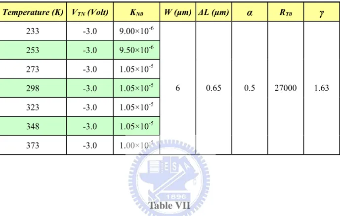
does not vary seriously for different gate voltages, so it can regarded as a constant for some device.parasitic resistance modeling results of the Poly-Si TFT’s with LDD structure are obtained. In order to get the clearer comparison results, both the extracted resistance and the modeling resistance are taken for the reciprocal to get the value of the conductance. The comparison between the extracted conductance values and the modeling conductance values is depicted in Fig.3-12 to Fig.3-17, respectively. From these figures, excellent agreement over the wide range of gate voltage and temperature between the extracted parasitic resistance and the modeling parasitic resistance is obtained. The all model parameter values of the proposed parasitic resistance model for the Poly-Si TFT’s with various LDD lengths are summarized in Table II to Table VII.
3.3 Modeling of Transfer Characteristics
Once again, the transfer characteristics are re-simulated by adopting the field effect mobility modeling results of the proposed mobility model for the Poly-Si TFT without LDD structure and the parasitic resistance modeling results of the proposed parasitic resistance model for the Poly-Si TFT’s with LDD structure. The calculation method to get the simulated drain current of the device with LDD structure is shown as:
P DS T GS OX FET DS DS R V V V C W L V I + ⎟ ⎠ ⎞ ⎜ ⎝ ⎛ − − ⋅ ⋅ ⋅ = 2 1
μ
(3-6)where
μ
FET is the mobility modeling results for the device without LDD structure and RP is the parasitic resistance modeling results for the device with LDD structure.The transfer characteristics simulation results for the Poly-Si TFT’s with LDD structure are shown in Fig.3-18 to Fig.3-23, respectively. Good agreement over the wide range of gate voltage and temperature between the raw measured transfer characteristic data and the modeling transfer characteristic results is also achieved.
Chapter 4
Conclusion
In this thesis, the Poly-Si TFT’s were fabricated by excimer laser annealing (ELA) recrystallization technology and the measurement work was done for the Poly-Si TFT’s of the same channel width and channel length with different LDD lengths at small drain bias under various environment temperatures.
For the Poly-Si TFT without LDD structure, the field effect mobility is extracted from the measured transfer characteristics and modeled by the proposed mobility model. The proposed mobility model has taken thermionic emission effect and phonon scattering effect into account, so it can provide reliable predictions for mobility variation under various temperatures. Good agreement over the wide range of gate voltage and temperature between the extracted mobility and the modeling mobility for the Poly-Si TFT without LDD structure is obtained. In addition, the transfer characteristics are also modeled by adopting the mobility modeling results of the proposed mobility model and good agreement over the wide range of gate voltage and temperature between the measured transfer characteristics and the modeling transfer characteristics for the Poly-Si TFT without LDD structure is also obtained.
Next, the parasitic resistance effect due to LDD structure is discussed. The parasitic resistance caused by LDD structure is calculated by subtracting the device resistance of the Poly-Si TFT without LDD structure from the device resistance of the Poly-Si TFT’s with LDD structure. According to the extracted parasitic resistance data, it is found that the parasitic resistance is modulated by gate bias and the modulation is more serious for the Poly-Si TFT’s with shorter LDD lengths.
After that, the device simulation results which are performed by Silvaco TCAD for the device with LDD structure show that parasitic transistor effect exists alongside the gate
electrode. The current path extends from the channel region into the LDD region due to the extended vertical electric field from the side of the gate electrode and then causing the extended channel length. The extended channel length is regarded as the channel length of the parasitic transistor and the parasitic transistor is also dominated by thermionic emission effect in temperature response. Besides, the resistance is treated as a pure resistor with a constant resistance at some temperature for the LDD region without gate bias modulation. Due to the higher doping concentration in LDD region than in channel region, plenty of the ionized space charges exist in LDD region. Therefore, the mechanism of the temperature response in this series resistance region is preferred to be considered as impurity scattering effect.
Finally, the proposed parasitic resistance model is established basing on the analysis and the assumptions mentioned above. The parasitic resistance modeling of the Poly-Si TFT’s with LDD structure is performed by using the proposed parasitic resistance model. Good agreement over the wide range of gate voltage and temperature between the extracted parasitic resistance and the modeling parasitic resistance is obtained. In addition, the transfer characteristics are re-simulated by adopting the mobility modeling results of the proposed mobility model for the Poly-Si TFT without LDD structure and the parasitic resistance modeling results of the proposed parasitic resistance model for the Poly-Si TFT’s with LDD structure. Good agreement over the wide range of gate voltage and temperature between the measured and the modeling transfer characteristics is also achieved for the all devices with LDD structure.
Appendix
The Proposed Mobility Model for Poly-Si TFT’s
There are two main mechanisms to affect the mobility of Poly-Si TFT’s. The first one is thermionic emission effect, and that introduces the effect of the activation energy (EA) which stands for the energy barrier height (EB) at grain boundaries. The other one is phonon scattering effect due to lattice thermal vibration. At small gate biases, the grain barrier height is still large and influences the mobility very seriously. The free carriers transport through the grain boundaries by thermionic emission, so the mobility increases as the temperature increases at small gate biases. On the contrary, at large gate biases, the energy barrier height at grain boundaries is almost suppressed by gate-induced charges. Thus, the dominated mechanism of mobility is changed to phonon scattering and mobility will decrease with increasing temperature. In fact, phonon scattering effect is also observed in single crystalline silicon.
As discussed above, the mobility of Poly-Si TFT’s is dominated by the grain barrier height at small gate biases, and the main conduction mechanism through the grain boundaries is thermionic emission over the grain-boundary energy barrier height. The equation can be generally written as:
⎟ ⎠ ⎞ ⎜ ⎝ ⎛ − ⋅ = kT EA G GB
μ
expμ
(A-1) whereμ
GB is the carrier mobility at the grain boundary regions;μ
G is the carrier mobility at the intra-grain regions;EA is the activation energy, or the energy barrier height at grain boundaries; k is Boltzmann constant.
However, the above formula can be refined to introduce the significance of the grain size and the grain boundary size. A linear relation between the field effect mobility and the grain size was observed. Therefore, the model equation can be improved by including a new term LG / LGB to describe the effect of the grain size and the grain boundary size on the field effect mobility.
Fig.A-1 is the illustration diagram for the derivation of the mobility model equation. It is assumed that the whole Poly-Si film is composed of the identical grain regions and the identical grain boundary regions in periodical structure. Furthermore, the assumption that each of them has an equivalent resistance and the all grain regions and the all grain boundary regions can be combined by Ohm’s Law is also presented. The derivation of the model equation is provided below:
⎟ ⎟ ⎟ ⎟ ⎠ ⎞ ⎜ ⎜ ⎜ ⎜ ⎝ ⎛ + = + = + = GB GB G G ch ch GB GB G ch G G G GB G G G ch L L Wnqt L W nqt L L L W nqt L L L R L L R L L R
μ
μ
μ
μ
1 1 ⎟ ⎟ ⎟ ⎟ ⎠ ⎞ ⎜ ⎜ ⎜ ⎜ ⎝ ⎛ + × = = = ⎟ ⎟ ⎟ ⎟ ⎠ ⎞ ⎜ ⎜ ⎜ ⎜ ⎝ ⎛ + = = GB G G GB GB G GB DS ch DS ch G GB G GB GB G GB G ch DS ch DS D L L L L qn L V J Wt L V JWt L L L L qnt L W V R V Iμ
μ
μ
σ
μ
μ
μ
μ
1If the dominated mechanism of the mobility is regarded as thermionic emission effect, then the Eq.(A-1) can be used in substitution for the term
μ
G. Therefore, the effective mobility to describe thermionic emission can be written as:⎟ ⎠ ⎞ ⎜ ⎝ ⎛ − ⋅ ⋅ = ≈ ⎟ ⎠ ⎞ ⎜ ⎝ ⎛ − + = + = kT E L L L L kT E L L L L L L L L A G GB G GB G GB A GB G GB G GB GB G G GB GB G GB TE exp exp 1 1
μ
μ
μ
μ
μ
μ
μ
(A-2) whereLG is the grain size of the Poly-Si film;
LGB is the grain boundary size of the Poly-Si film;
μ
G is the carrier mobility at the intra-grain regions;EA is the activation energy, or the energy barrier height at grain boundaries; k is Boltzmann constant;
T is the environment temperature with the unit of Kelvin;
Besides, if the mobility is dominated by phonon scattering effect, the equation is generally given as:
β
μ
μ
− ⎟⎟ ⎠ ⎞ ⎜⎜ ⎝ ⎛ ⋅ = 0 0 T T T PS (A-3) whereμ
T0 is the constant mobility at high gate biases at 298K; T is the environment temperature with the unit of Kelvin;T0 is the reference temperature which defined as the room temperature, 298K;
β
is the temperature dependence coefficient to describe phonon scattering effect.The value of
β
for single crystalline silicon is 3/2. While approaching to this value more, the crystal quality of the intra-grain region in Poly-Si film is closer to single crystalline silicon. After deriving the mobility equations for thermionic emission effect and phonon scattering effect, the completed mobility model can be finally written as:β
μ
μ
μ
μ
μ
− ⎟⎟ ⎠ ⎞ ⎜⎜ ⎝ ⎛ ⋅ + ⎟ ⎠ ⎞ ⎜ ⎝ ⎛ − ⋅ ⋅ = + = 0 0 1 exp 1 1 1 1 T T kT E L L T A G GB G PS TE eff (A-4)Besides, oxide-silicon interface scattering effect also has to be considered. A common empirical form to describe interface scattering effect is used in the proposed mobility model. Then, the final field effect mobility can be given as:
(
GS T)
eff FET V V − ⋅ + =θ
μ
μ
1 (A-5)where
θ
is the gate bias dependence coefficient to describe oxide-silicon interface scattering effect and VT is the threshold voltage of device.Afterward, the extracted mobility values of the N-type and P-type long channel devices are modeled by the proposed mobility model, respectively. Although the devices used in this section were recrystallized by ELA method with 420 mJ / cm2 laser energy, the same as the devices used in chapter 2 and chapter 3, but they were fabricated in different runs, so the device performance of these devices is very different.
First, the 6μm channel width and 30μm channel N-type Poly-Si TFT with 0.5μm LDD length and the 6μm channel width and 30μm channel P-type Poly-Si TFT without LDD structure are checked, respectively. The mobility modeling results for both is shown in Fig.A-2 and Fig.A-3, and good agreement is obtained. It is obvious that the field effect mobility of the P-type Poly-Si TFT is dominated by phonon scattering effect more strongly than the N-type Poly-Si TFT. The model parameters of the proposed mobility model for the N-type TFT and the P-type TFT are summarized in Table VIII and Table IX, respectively.
The temperature dependence of the model parameters VT and
μ
G / LGB is also checked. The relation between the threshold voltage VT and the temperature and the relation between the parameterμ
G / LGB and the temperature for the N-type TFT and the P-type TFT are shown in Fig.A-4 and Fig.A-5, respectively. The near-linear relation is observed for the both parameters in the N-type TFT and the P-type TFT. Thus, the linear equation can be both used to describe the temperature dependence of the two parameters, and the inconvenience of the model parameter adjusting is alleviated.References
[1] A. G. Lewis, I-W. Wu, T. Y. Huang, A. Chiang and R. H. Bruce, “Active matrix liquid crystal display design using low and high temperature processed polysilicon TFTs,” IEDM Tech. Dig., pp. 843-846, 1990
[2] Y. Matsueda, M. Ashizawa, S. Aruga, H. Ohshima and S. Morozumi, soc. Information Display, Tech. Dig., pp. 315-318, 1990.
[3] R. G. Stewart, S. N. Lee, A. G. Ipri, D. L. Jose, D. A. furst, S. A. Lipp and W. R. Roach, “A 9V polysilicon LCD with integrated gray-scale drivers,”
soc. Information Display, Tech. Dig., pp. 319-322, 1990.
[4] T. Yamanaka, T. Hashimoto, N. Hasegawa, T. Tanaka, N. Hashimoto, A. Shimizu, N. Ohki, K. Ishibashi, K. Sasaki, T.Nishida, T. Mine, E. Takeda and T. Nagano, “Advanced TFT SRAM Cell Technology Using a Phase-Shift Lithography,” IEEE Trans. Electron Devices, Vol. 42, No. 7, pp. 1305-1313, 1995.
[5] S. D. S. Malhi, H. Shichijio, S. K. Banerjee, R. Sundaresan, M. Elahy, G. P. Polack, W. F. Richardaon, A. H. Shah, L. R. Hite, R. H. Womoack, P. K. Chatterjee and H. W. Lan, “Characteristics and Three-Dimensional Integration of MOSFETs in Small-Grain LPCVD Polycrystalline Silicon,”
IEEE Trans. Electron Devices, Vol. 32, No. 2, pp. 258-281, 1985.
[6] K. YoShizaki, H. Takahashi, Y. Kamigaki, T.Yasui, K. Komori and H. Katto, ISSCC Digest of tech. Papers, pp. 166, 1985.
[7] N. D. Young, G. Harkin, R. M. Bunn, D. J. McCullloch and I.D. French, “The Fabrication and Characterization of EEPROM Arrays on Glass Using a Low-Temperature Poly-Si TFT Process,”
[8] T. Serikawa, S. Shirai, A. Okamoto and S. Suyama,
“Low-temperature fabrication of high-mobility poly-Si TFTs for large-area LCDs,” IEEE Trans. Electron Devices, Vol. 36, pp. 1929-1933, 1989.
[9] T. Noguchi, “Appearance of single-crystalline properties in fin-patterned Si TFTs by solid phase crystallization,”
Jpn. J. Appl. Phys., pt. 2, Vol. 32, No. 11A, pp. 1584-1587, 1993.
[10] S. W. Lee and S. K. Joo. “Low temperature poly-Si thin film transistor fabrication by metal-induced lateral crystallization,”
IEEE Electron Device Lett., Vol. 17, pp. 160-162, 1996.
[11] N. Kuno, N. Kusumoyo, T. Insushima and S. Ymaazaki, “Characterization of
polycrystalline-Si thin-film transistor fabricated by excimer laser annealing method,” IEEE Trans. Electron Devices, Vol. 40, pp. 1876-1879, 1994.
[12] M. D. Jacunski, M. S. Shur, A. A. Owusu, T. Ytterdal, M. Hack and B. Iniguez, “A Short-Channel DC SPICE Model for Polysilicon Thin-Film Transistors Including Temperature Effects,” IEEE Trans. Electron Devices, Vol. 46, No. 6, 1999.
[13] Apostolos T. Voutsas, “Assessment of the Performance of
Laser-Based-Lateral-Crystallization Technology via Analysis and Modeling of Polysilicon Thin-Film-Transistor Mobility,”
IEEE Trans. Electron Devices, Vol. 50, No. 6, 2003.
[14] Chang-Yu Huang, “The Crystallization Mechanism and the Mobility Model of Poly-Si TFTs annealed by Solid-State Nd:YAG Laser,”
Table I
The model parameter values of the proposed mobility model for the W/L = 6μm / 6μm N-type Poly-Si TFT without LDD structure
Temperature (K) VT (Volt)
μG
/ LGB LG (μm)μT0
β
θ
233 -1.725 400 253 -1.866 420 273 -1.970 440 298 -2.126 460 323 -2.231 480 348 -2.384 500 373 -2.481 520 0.8 152 0.12 0.012Table II
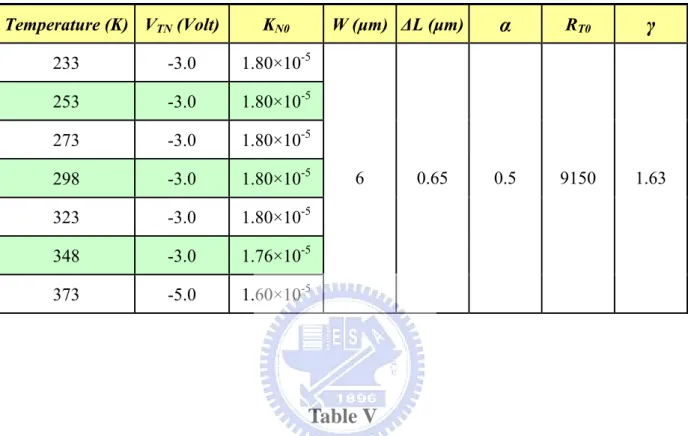
The model parameter values of the proposed parasitic resistance model for the W/L = 6μm / 6μm N-type Poly-Si TFT with 0.5μm LDD length
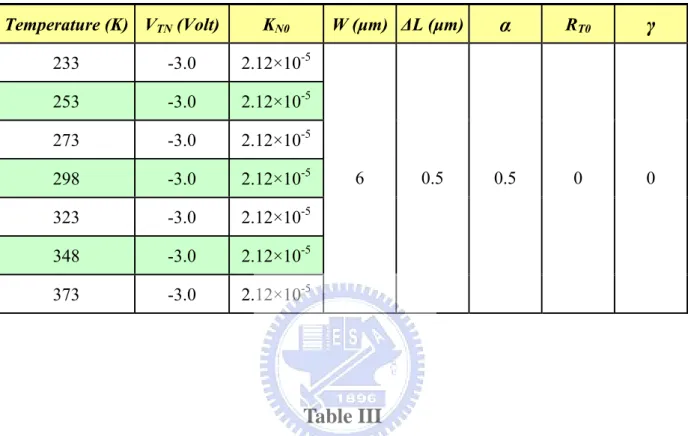
Table III
The model parameter values of the proposed parasitic resistance model for the W/L = 6μm / 6μm N-type Poly-Si TFT with 1.0μm LDD length
Temperature (K) VTN (Volt) KN0 W (μm) ΔL (μm)
α
RT0γ
233 -3.0 2.12×10⁻⁵ 253 -3.0 2.12×10⁻⁵ 273 -3.0 2.12×10⁻⁵ 298 -3.0 2.12×10⁻⁵ 323 -3.0 2.12×10⁻⁵ 348 -3.0 2.12×10⁻⁵ 373 -3.0 2.12×10⁻⁵ 6 0.5 0.5 0 0 Temperature (K) VTN (Volt) KN0 W (μm) ΔL (μm)α
RT0γ
233 -3.0 1.80×10⁻⁵ 253 -3.0 1.80×10⁻⁵ 273 -3.0 1.80×10⁻⁵ 298 -3.0 1.80×10⁻⁵ 323 -3.0 1.80×10⁻⁵ 348 -3.0 1.76×10⁻⁵ 373 -5.0 1.60×10⁻⁵ 6 0.65 0.5 3850 1.63Table IV
The model parameter values of the proposed parasitic resistance model for the W/L = 6μm / 6μm N-type Poly-Si TFT with 1.5μm LDD length
Table V
The model parameter values of the proposed parasitic resistance model for the W/L = 6μm / 6μm N-type Poly-Si TFT with 2.0μm LDD length
Temperature (K) VTN (Volt) KN0 W (μm) ΔL (μm)