低電壓5-GHz互補式金氧半電晶體直接降頻式射頻前端接收器
103
0
0
全文
(2) 低電壓5-GHz 互補式金氧半電晶體 直接降頻式射頻前端接收器 DESIGN OF LOW VOLTAGE 5-GHz CMOS DIRECT-CONVERSION FRONT-END RECEIVER. 研 究 生:丁. 彥. 指導教授:吳重雨. Student:Yen Ding Advisor:Chung-Yu Wu. 國 立 交 通 大 學 電機資訊學院 電子與光電學程 碩 士 論 文. A Thesis Submitted to Degree Program of Electrical Engineering Computer Science College of Electrical Engineering and Computer Science National Chiao Tung University in Partial Fulfillment of the Requirements for the Degree of Master of Science in Electronics and Electro-Optical Engineering July 2004 Hsinchu, Taiwan, Republic of China. 中華民國九十三年七月.
(3) 低電壓 5-GHz 互補式金氧半電晶體 直接降頻式射頻前端接收器 學生:丁 彥. 指導教授:吳重雨 教授. 國立交通大學電機資訊學院 電子與光電學程﹙研究所﹚碩士班. 摘. 要. 低耗電與高資料傳輸特性使得無線區域網路的發展日漸蓬勃,在無線區域網 路 802.11a 規格頻譜中,特別將 52 個次頻道中,保留編號 0 的次頻道不予發送, 這對於選用架構簡單的直接移頻接收器十分有利,並且也增加了單晶片整合的機 會。本論文使用互補式金氧半電晶體製作一個直接移頻接收器,透過國家晶片系 統設計中心,以臺灣積體電路製造股份有限公司提供的 0.18 μm 製程技術實 現。論文最大的重點在於處理直接移頻架構的自我混波問題,提出一個新的準位 偏移補償電路,並當作混波器的負載,直接消除因自我混波所產生的直流準位偏 移電壓。射頻接收器所含電路有低雜訊放大器、正交壓控振盪器及降頻器。 量測結果顯示,所設計的射頻前端接收器可於 1.1 V 電源下正常運作。射頻 接收器在規範的頻寬中均有–15 dB 輸入反射因數、17.8 dB 電壓增益、14.9 dB 雜訊指數、–23 dBm 之 1 dB 增益壓縮點,當接收器輸入端灌入一組與振盪器同 頻且強度為-50 dBm 的信號時,其自我混波後的直流準位偏移電壓為 1 ~ 3 mV。 此外,接收器消耗功率為 37.56 mW,晶片面積為 2.09 mm2。. -i-.
(4) DESIGN OF LOW VOLTAGE 5-GHz CMOS DIRECT-CONVERSION FRONT-END RECEIVER Student:Yen Ding. Advisor:Prof. Chung-Yu Wu. Degree Program of Electrical Engineering Computer Science National Chiao Tung University. ABSTRACT. Wireless local network is a fast growing market that enables lower power dissipation and higher data rates. The IEEE 802.11a standard which channel 0 is useless among 52 sub-carriers; this is favorable for direct-conversion architecture. This thesis proposes a CMOS direct-conversion receiver, and is realized by TSMC 0.18 μ m technology via Chip Implementation Center. The major issue in the direct-conversion architecture is self-mixing problem; a new offset compensation circuit is used as the mixer loads to alleviate the DC offset. The receiver comprises a low-noise-amplifier, a quadrature voltage-controlled oscillator and downconverter. Measured results reveal that the designed receiver can operate well at 1.1 V power supply. It performs –15 dB input refection coefficient in interesting band, 17.8 dB conversion gain, 14.9 dB noise figure, -23 dBm 1 dB compression point. The DC offset voltage is 1 ~ 3 mV with input injected power of –50 dBm. It consumes 37.56 mW and die area is 2.09mm2. - ii -.
(5) 誌 謝. 能夠順利畢業,要感謝的人實在很多。首先,要對我的指導教授吳重雨老師 致上最誠摯的感謝。老師在這二年裡不論在硬體或是軟體上提供了我一個最佳的 學習環境。在學習上老師也給予了適時的指導與啟發,使我不在錯誤當中打轉, 更教導了我許多做事的方法與態度。 其次我要感謝實驗室的學長高宏鑫、鄭秋宏、廖以義、施育全、周忠昀、林 俐如、黃冠勳、江政達、王文傑、虞繼堯、蘇烜毅、蔡俊良、李彥伯、黃柏獅、 劉沂娟的努力,才使實驗室軟硬體設備一應俱全。在如此的環境下,我的論文才 能順利完成。再來我要感謝實驗室的同學:吳瑞仁、蘇芳德、鄭建祥、張秦豪、 許德賢、謝致遠、陳旻珓、陳勝豪、林韋霆、杜長慶、蘇紀豪、楊文嘉、李宗霖、 邱偉茗、林大新、王騰毅、張家華、曾偉信、阿爛、黃如琳、郭秉捷、張瑋仁、 林棋樺、李權哲、周政賢、蕭聖文、陳正瑞、陳政良、陳煒明……等,研究功課 或外出遊玩,陪伴著我一起渡過了這二年的研究生涯。 還有我的同梯蔡裕文,由於他的鼓勵,我才會來攻讀碩士學位,做電路設計, 衷心感謝。最後我要感謝我的家人,對我放棄工作來唸書的支持,使我在學習之 餘無後顧之憂。 其他要感謝的人還有很多,無法一一列出,在此一併謝過。 丁 彥 國立交通大學 中華民國九十三年七月. - iii -.
(6) Contents Chinese Abstract…………………………………………….i English Abstract…………………………………………….ii Contents……………………………………………………..iv Table Captions………………………………………………vi Figure Captions...…………………………………………viii. CHAPTER 1. INTRODUCTION…………………………..1. 1.1. BACKGROUND…………………………………………………………….1. 1.2. REVIEW ON CMOS RF FRONT-END RECEIVER………………………...2 1.2.1. Receiver Architectures…………………………………………...3. 1.2.2. Issues of Direct-Conversion……………………………………..6. 1.2.3. Low-Voltage Receivers………………………………………….10. 1.3. MOTIVATIONS ..………………………………………………………….11. 1.4. THESIS ORGANIZATION………………………………………………….12. CHAPTER 2. DOWNCONVERTER WITH DC OFFSET COMPENSATION……………………….13. 2.1. OPERATIONAL PRINCIPLE………………………………………………..13. 2.2. DESIGN CONSIDERATIONS……………………………………………….15 2.2.1. DC Offset Compensation………………………………………..15. 2.2.2. Band-Pass Filter………………………………………………….18. 2.2.3. Voltage Conversion………………………………………………20 - iv -.
(7) 2.2.4. Noise and Linearity………………………………………………22. 2.3. CIRCUIT REALIZATION……………………………………………………24. 2.4. SIMULATION RESULTS ON DOWNCONVERTER…………………………..26. CHAPTER 3. 1-V 5-GHz DIRECT-CONVERSION FRONT-END RECEIVER……………….31. 3.1. IEEE 802.11a PHY STANDARD AND LINK BUDGET……………………32. 3.2. CIRCUIT REALIZATION…………………………………………………….35. 3.3. 3.2.1. Differential Low Noise Amplifier…………………………………35. 3.2.2. Quadrature Voltage-Controlled Oscillator ……………………..43. 3.2.3. Output Buffer ……………………………………………………..45. SIMULATION RESULTS ON FRONT-END RECEIVER………………………47. CHAPTER 4. EXPERIMENTAL RESULTS……………57. 4.1. LAYOUT DESCRIPTION……………………………………………………57. 4.2. MEASUREMENT SETUP AND CONSIDERATIONS………………………….59. 4.3. EXPERIMENTAL RESULTS ………………………………………………..64. 4.4. DISCUSSIONS AND COMPARISONS……………………………………….72. CHAPTER 5. CONCLUSIONS AND FUTURE WORKS…………………………………..84. 5.1. CONCLUSIONS……………………………………………………………84. 5.2. FUTURE WORKS………………………………………………………….85. REFERENCES………………………………………………86 -v-.
(8) Table Captions Table 1-1 Comparison on DC offset removal methods………………………………..8 Table 2-1 Parameter information of Fig. 16.…..……………………………………..26 Table 2-2 Relative corner frequency of Fig. 18..…………………………………….27 Table 2-3 Post-simulation summary of the downconverter.…………………………30 Table 3-1 IEEE 802.11a specification for this thesis required ………………………34 Table 3-2 Design target of the front-end receiver and each circuit..…………………35 Table 3-3 Parameter information of Fig. 30..………………………………………..43 Table 3-4 Parameter information of Fig. 34……..……………..……………….……45 Table 3-5 Post-simulation summary of the LNA ..…………………………………..49 Table 3-6 Post-simulation summary of the quadrature VCO ..………………………51 Table 3-7 DC offset information of Fig. 47…..………………………………….…..53 Table 3-8 Corner-case simulation summary of the receiver..…………………….….55 Table 3-9 Post-simulation summary of the front-end receiver..………………….….56 Table 4-1 Comparison on gate biases and bias resistor..………………………….…71 Table 4-2 Summary of the tested receiver ………….…………………………….…71 Table 4-3 Related parasitical resistors of QVCO………………………………..…..73 Table 4-4 Comparison on start of oscillation condition ……………….…………….74 Table 4-5. The related parasitical resistors of LNA.. ………………………………..75 Table 4-6 Comparison on the re-design parameter…………………………………..77 Table 4-7 Performance parameter of each sub-circuit ……………………………….78 Table 4-8 Post-simulation summary of re-design receiver …………………………..79 Table 4-9 Comparison with other 5-GHz receiver …………………………………..80 Table 4-10 Comparison on DC offset removal design ………………………………81 Table 4-11 Performance comparisons with IEEE 802.11a specification…………….81. - vi -.
(9) Table 4-12 Post-simulation summary of modified design……………………………83. - vii -.
(10) Figure Captions Figure 1. A common receiver architecture…………………………………………….2 Figure 2. Architecture of heterodyne receiver.………………………………………..3 Figure 3. Architecture of homodyne receiver…………………………………………4 Figure 4. Self-mixing of LO leakage and interferer leakage...………………………..6 Figure 5. Receiver architecture in this thesis ………………………………………..12 Figure 6. Basic cell X ………………………………………………………………..14 Figure 7. Basic cell Y constructed by two basic cells X……………………………..14 Figure 8. Double-balanced structure…………………………………………………15 Figure 9. Simple example for dc offset observation…………………………………16 Figure 10 DC offset reducing circuit…………………………………………………17 Figure 11 A band-pass filter as downconverter load..………………………………..18 Figure 12. Band-pass impedance frequency spectrum……………………………….20 Figure 13. Realization of basic cell X………………………………………………..20 Figure 14. Realizations of basic cell Y……………………………………………….21 Figure 15. Realizations of double-balanced combiner……………………………….21 Figure 16. Double-balanced downconverter with DC offset compensation circuit (a) I-channel (b) Q-channel………………………………………………25 Figure 17. Simulated voltage conversion gain of the downconverter………………..26 Figure 18. Voltage gain versus frequency on gain variations ..………………………27 Figure 19. Output noise voltage spectral density of downconverter..………………..28 Figure 20. Extrapolation of downconverter IIP3………………..……………………29 Figure 21 DC offset voltage caused by injected leakage powers ..…………………..29 Figure 22. Block diagram of direct-conversion receiver……………………………..31 Figure 23. IEEE 802.11a lower frequency band of the channel allocation..…………32. - viii -.
(11) Figure 24. Input impedance matching ..…….………………………………………..36 Figure 25. Modified impedance model ..…………………………………………….37 Figure 26. Impedance Smith chart ..…………………………………………………37 Figure 27. Noise model of input stage……………………………………………….38 Figure 28. NFmin curves to W and Pc……...………………………………………….40 Figure 29. Intermodulation phenomenon.……………………………………………40 Figure 30. Designed LNA circuit ..…………………………………………………..42 Figure 31. General resonator……………………………………………………..…..43 Figure 32. Conceptual diagram of the quadrature voltage-controlled oscillator..……44 Figure 33. Inverter circuit applied in the quadrature voltage-controlled oscillator ….44 Figure 34. Quadrature voltage-controlled oscillator..………………………………..45 Figure 35. One channel of the output buffer circuit.…………………………………46 Figure 36. Frequency response of output buffer ..…..……………………………….46 Figure 37. Simulated S11 of the LNA………………………………………………..48 Figure 38. Simulated voltage gain of the LNA………………………………………48 Figure 39. Simulated noise figure of the LNA……………………………………….48 Figure 40. Two-tone-test plot for simulated IIP3 of the LNA………………………..49 Figure 41. Differential output of LO spectrum ..…………………………………….50 Figure 42. Quadrature LO waveform (solid-line:I-channel;dash-line:Q-channel)..50 Figure 43. Simulated VCO tuning range ..……………………..…………………….50 Figure 44. Simulated I-channel and Q-channel IF waveform………………………..52 Figure 45. Two-tone-test plot for simulated IIP3 of the receiver..……….…………..52 Figure 46. Output noise voltage spectral density of receiver ..………………………52 Figure 47. DC offset at each sub-circuit with differential output ……………………53 Figure 48. Monte Carlo simulation with only LNA channel-length variations………53 Figure 49. Monte Carlo simulation with LNA and Mixer channel-length variations..54 - ix -.
(12) Figure 50. Monte Carlo simulation with whole receiver channel-length variations....54 Figure 51. The receiver layout..………….…………………………………………..58 Figure 52. Chip microphotographs……………….…………………………………..59 Figure 53. Bonding board for the receiver ..…..……………………………………..60 Figure 54. The half circuits of input matching network ……………………………..61 Figure 55. Photograph of matching network ………….……………………………..61 Figure 56. Adjustable voltage modules……………………………..………………..61 Figure 57. DC board for the bonding board of receiver..…………………………….62 Figure 58. (a) The receiver chip integrated with discrete component.……………….62 (b) The receiver chip integrated with discrete component……………….63 Figure 59. Using bypass capacitors to obtain stable LO..……………………………64 Figure 60. Loss of balun and micro-strip line………………..………………………65 Figure 61. Loss of transformer and DC blocking capacitor………………………….65 Figure 62. Apparent S11 of the receiver ..……………………………………………65 Figure 63. Spectrum of LO leakage………….………………………………………66 Figure 64. QVCO tuning-range plot..………………………………………………..66 Figure 65. The IF spectrum.………………………………………………………….67 Figure 66. Quadrature IF output waveforms of receiver ..…………..……………….68 Figure 67. IF output waveform with 10 KHz ..………..……………………………..68 Figure 68. Measured receiver conversion gain ..…….………………………………68 Figure 69. Measured spectrum of noise figure……………………………………….69 Figure 70. Two-tone IIP3 measurement for the receiver..……………………………69 Figure 71. Measurement of receiver DC offset voltage..…………………………….70 Figure 72. Conceptual diagram of the QVCO with parasitical effect ..……….……..72 Figure 73. Equivalent inductance in the QVCO ……………………………………..73 Figure 73. Equivalent inductance in the QVCO ……………………………………..73 -x-.
(13) Figure 74. Equivalent Q value in the QVCO ....……………………………………..74 Figure 75. Conceptual diagram of the LNA with parasitical effect ..………………..75 Figure 76. Conversion gain of re-simulation...………..……………………………..75 Figure 77. DC offset voltage of re-simulation...……………………………………..76 Figure 78. Noise figure of re-simulation……………………………………………..76 Figure 79. 1-dB compression point of re-simulation.………………………………..76 Figure 80. Conceptual diagram of decouple the current in QVCO and downconverter ………………………………………………………….80. - xi -.
(14) CHAPTER 1 INTRODUCTION. 1.1 BACKGROUND As the vigorous development of wireless communication systems, many related application products have been promoted. The current trend of those products is towards integrated circuits on single chip and the RF IC played the leading role in the wireless communication systems. Besides supplying more functionality, any useful RF IC solution also orientates to more small, costless, and power saver. Performance, cost, and time to market are three critical factors influencing the choice of technologies in the competitive RF industry. CMOS technology has low cost and high fabrication turnaround time make it desirable to use a single mainstream digital CMOS process for all IC products [1]. Based on CMOS techniques contribute architectural innovations in the wireless systems may lead to revolutionary improvements. The RF section of new phones has experienced significant size reduction due to evolution of RF architecture [2]. Many of practical RF architectures have their significant characteristic, an optimum design method is considering the entire communication systems including both RF and baseband functionalities, choosing the proper sub-blocks. Wireless equipments with high performance depend on proper-designed circuit in accordance with specification defined, such as GSM and GPRS for mobile communication or Bluetooth and IEEE 802.11 family for wireless local area network. RF circuit is usually a main of bottlenecks, even if they occupy only a small part in the overall. Mobility is at the heart of wireless communications. Many wireless communication. -1-.
(15) systems will emerge to serve special needs that are not met well by the existing system. Without the challenge of mobility, they are able to achieve higher spectrum efficiency and other economies relative to wireless systems that serve mobile subscribers [3]. It is difficult to grasp the analogy and high-frequency characters in the RF circuit design. Researcher should carefully investigate on material, lithography, parasitical elements, choosing architecture and other ways to overcome the existent obstacles. As plenty studies bring lots of efficient development, more and more wireless equipments have become commercial and popular products.. 1.2 REVIEW ON CMOS RF FRONT-END RECEIVER The transceiver is a quite major component in the wireless communication equipment that includes commonly receiver, transmitter and frequency synthesizer. RF front-end receiver generally consists of several main components: Low-noise amplifier (LNA), Downconverter and Filter. LNA amplifies RF signal received from antenna with low noise contribution. Downconverter mixes RF signal amplified by LNA with LO signal generated by VCO and outputs interested frequency signal to feed subsequent circuit stage. Filter suppresses undesired signal for baseband circuit receiving message of sufficiently low error rate. Fig 1 enumerates one of receiver architectures for example. LO. DSP. RF LNA. RF Filter. Downconverter. IF Filter. RF. LO. Fig. 1 A common receiver architecture. -2-. Baseband.
(16) Wireless communication is a narrow-band system, which usually suffers from nonlinearity issues while signals of various frequencies are received simultaneously; intermodulation phenomenon corrupts the adjacent-channel signal [4]. It is hard to suppress the undesired intermodulated signal by any existent filter. Complexity, cost, power dissipation, and number of external components have been the primary criteria in selecting receiver components. In the past, heterodyne is the architecture that is selected for the most of the cellular handsets due to its high performance [5], but a lot of its components is still needed to be discrete. There are special issues on different architectures that will be discussed in the following:. 1.2.1 Receiver Architectures As RF receiver is evolving continuously, several architectures in recent years can be generalized. The-well-know architectures are heterodyne receiver, homodyne receiver and low-IF/ image-reject receiver [4]. A. Heterodyne receiver Heterodyne receiver downconverts the received RF signal to interested intermediate frequency (IF), which is usually much lower than the initially received frequency band. The heterodyne receiver is illustrated in Fig. 2. LO. BPF. BPF. BPF IF Output. Band-Select Filter. LNA. Im age Reject Filter. Downconverter. ChannelSelect Filter. Fig. 2 Architecture of heterodyne receiver This topology leads to the severe tradeoff between sensitivity and selectivity [4]. A high IF increases the difference frequency between image and desired signal and gets a better image-rejection performance, but this need a channel-selection filter with very high Q-factor. It is difficult to design a filter of sufficiently high Q-factor on chip. Even -3-.
(17) if integrated image-reject filter is realized in practice [6]. This is not suitable for low power design. If the IF is low, the channel-selection filter has a more relaxed requirement, but proper image suppression becomes harder to achieve. To relax the trade-off, dual-IF topology is applied [7], but it has power-consumption issue due to more circuit stage for multi-downconversion procedure. Compared to other topologies, heterodyne receiver can achieve better performance; but it is more complexity, difficult integration and not appropriate to different wireless standards and modes. B. Homodyne receiver The homodyne receiver also called zero-IF or direct-conversion which avoids the disadvantages of the heterodyne architecture by converting the RF signal directly to baseband. It translates the channel of interest directly to zero frequency in one step by mixing with an LO output of the same frequency. A low-pass filter that is used to suppress nearby interferers filters the resulting baseband signal. The homodyne receiver is illustrated in Fig. 3. LO. B PF. B PF IF O utput. Band-Select F ilter. LNA. Dow nconverter. C hannel-Select F ilter. Fig. 3 Architecture of homodyne receiver The main advantage of homodyne receiver is the high integration, simplicity of structure, cost and power reduction. It avoids the need for an off-chip IF filter and requires only one single frequency synthesizer. The problem of the image is minimized, as the incoming RF signal is down-converted directly to zero, if the quadrature down-converter is used [8]. As result, no image-reject filter is required. The possibility of changing the bandwidth of the integrated low-pass filters (and thus, changing the -4-.
(18) receiver bandwidth) is the other advantage if multimode and multi-band applications are of concern [9]. The homodyne receiver also allow analog-to-digital converter (ADC) and digital signal processing (DSP) circuits to perform demodulation and other ancillary functions, relaxes the selectivity requirements if highly integrated, low-cost and low-power realization [5]. Homodyne receivers suffer impairment of DC offset, flicker noise, I/Q mismatch and even-order distortion. The effects of even-order distortions can generally be made sufficiently by negligible with good circuit techniques and I/Q mismatch is the biggest challenge in the implementation of CMOS frequency synthesizer. However, DC offset and flicker noise problems are generally considered much more serious and challenging to the designers. C. Low-IF/Image-reject receiver The low-IF topology starts from combined the advantages of both receiver types introduced above. The low-IF receiver is no DC offset problem but have image problems. The most common techniques to remove the image are to use IR architecture [10] or polyphase filter [11]. Furthermore, the signal bandwidth in low-IF conversion is twice that in direct conversion, therefore requires doubling the analog-to-digital conversion sampling rate, and results in higher power consumption. Finally, the double signal bandwidth in low-IF conversion mandates to double the baseband filter bandwidth, which further increases design complexity and power consumption [12]. One type of image-reject receiver is the Hartley architecture [13]. The main drawback of this architecture is that the receiver is very sensitive to mismatches due to phase and gain imbalance of the local oscillator signals, which causes incomplete image cancellation. Also, the loss and noise of the shift-by-90° stage and the linearity of the adder are critical parameters. Another type of image-reject receiver is the Weaver architecture [14]. Similar to the Hartley receiver, the image can no longer be cancelled -5-.
(19) completely if the two local oscillator signals are not perfect 90°. However, the Weaver architecture is also sensitive to mismatches, but it avoids the use of RC-CR network, thereby achieving greater image rejection despite process and temperature variation [2].. 1.2.2 Issues of Direction-Conversion The direction-conversion receiver entails a number of issues that consulted previously need to conquer in favor of full integration. A. DC offset The major disadvantage is that severe DC offset can be generated at the output of the mixer. DC offset in a homodyne receiver are illustrated in Fig. 4. The DC offset can be generated by self-mixing of the LO leakage signal with the LO signal [Fig. 4 (a)] or self-mixing of a strong interferer due to leakage from the LNA [Fig. 4 (b)]. The LO and interferer leakage arise from capacitive and substrate coupling. If self-mixing varies with time, it leads DC offset issue to be exacerbated. Undesired DC offset corrupts the baseband signal and saturate the following gain stages. Also, DC offset in I/Q signal paths shifts the baseband signal constellation, causing potential signal saturation, as well as degrading the bit error rate (BER) performance [15]. Moreover, the transistor mismatch in the signal path and demodulation of large amplitude modulated signal via second-order nonlinearity of the mixer that also generates DC offset. LO. LO Interferer Leakage. LO Leakage IF Output. LNA. IF Output. Downconverter. LNA. (a). Downconverter. (b). Fig. 4 Self-mixing of LO leakage and interferer leakage A solution for DC offset removal is to employ ac-coupling, i.e. high–pass filtering, in the down-converted signal path. Unfortunately, this solution removes the DC energy -6-.
(20) of desire signal. It requires prohibitively large capacitors or resistors and accompanies unavoidable in-band loss. A low corner frequency in the HPF may lead to temporary loss of data in the presence of wrong initial conditions, and result in long transient settling during gain changes or Tx-to-Rx switching [16]. There is similar way to withstand DC offset by ac-coupling and unity gain amplifier, but it must face the linearity issue simultaneously [17]. The dc-coupled with feedback configuration, using negative feedback around the baseband amplifier, is another topology to suppress the DC offset. It circumvents the disadvantages in the ac-coupling method. However, the gain of baseband amplifier is large and has a number of stages. It makes the feedback path with very large capacitance or the extremely small transconductance. Additionally, It is also constraint on stability in the circuit design [18][19][20]. Also, in the multi-phase reduced frequency conversion receiver architecture, the VCO frequency is reduced and deviated from the carrier frequency and the DC offset can be drastically reduced [21]. But it brings about complexities and symmetrization on circuit design, consumes extra power due to using multi-phase mixer and VCO. The architecture of balanced harmonic mixer can alleviate offset extremely, it uses second harmonic of the LO signal that takes part in the mixing process. As a result, the LO leakage generates no DC component but an output which is still situated at the LO frequency and can be easily filtered out [22][23]. The main issues of this architecture are its weakness on linearity and require higher LO strength due to use of second harmonic signal. Dynamic calibration and DSP techniques are other popular techniques employed to minimize signal degradation [12][24]. It uses DACs and lookup table (LUT) to calibrate static dc periodically and compensate for temperate fading. However, this requires extra DACs and LUT circuit. The operation and algorithm are complicated, the calibration is -7-.
(21) executed only in idle mode and no signal detected. An offset cancellation mixer can cancel offset by dynamically varying the bias on the loads, which are designed to provide constant impedance independent of the load cancellation current [25]. Nevertheless, the circuit needs extra two digital filter (ex: IIR) to detect dynamic offset. It also requires DACs and common-mode feedback (CMFB) circuits. This would consume more power and pay more attention to circuit stability. The comparison on DC offset removal methods are listed in Table 1-1. Generally, the offset cancellation circuit in a receiver should be simplification, power saving and erode performance few as far as it can. Table 1-1 Comparison on DC offset removal methods Reference. [17] [19] [21] [23] [12] [25]. Large C or R. ˇ. Long settling time and in-band loss. ˇ. ˇ. ˇ. Constraint on stability. ˇ. Weakness on linearity. ˇ. Required CMFB Sensitive to layout. ˇ. Architecture complexities. ˇ. ˇ. Require DACs ˇ. Consume extra power. ˇ. ˇ. ˇ. ˇ. ˇ. ˇ. ˇ. B. Flicker noise The flicker noise, also knows as 1/ƒ noise, is an intrinsic noise phenomenon found in semiconductor devices, especially in CMOS implementations. Flicker-noise property of a device is semiconductor dependent, and the corner frequency is typically in the vicinity of 1MHz for MOSFET devices [15]. Since the mixer output is down-converted -8-.
(22) to a baseband signal, it is quite sensitive to noise and easily be corrupted by the large flicker noise of the mixer. The flicker-noise effect can be minimized by proper selection of semiconductor processes with low corner frequency and providing adequate gain in the front end to improve relative signal-to-noise ratio (SNR) at the down-converter output. It also can incorporate very large device to minimize the magnitude of the flicker noise [4]. A two-stage mixer where the V/I converter and the switching quad biasing current can be independently optimized that achieves lower noise figure while maintaining the same conversion gain [26]. Since holes are less likely to be trapped, pMOSFETs have less flicker noise than nMOSFETS. C. I/Q mismatch I/Q mismatch, or phase and gain mismatch, introduced by the mixer is another critical issue for homodyne receiver topology. Gain error simply appears as a non-unity scale factor in the amplitude. Phase imbalance, on the other hand, corrupts each channel by a fraction of the data pulses in the other channel; in essence degrading the signal-noise ratio if the I and Q data streams are uncorrelated. Any mismatch distorts the constellation diagram of the baseband signal, resulting in an enhanced BER [4]. Tolerable gain and phase imbalance depends on modulations techniques employed in a system. For example, the use of 64-QAM modulations require a SNR of 30 dB, which is substantially greater than required by the FSK modulation in Bluetooth and the QPSK modulation in 802.11b. This high SNR translates to stringent phase noise requirements and tight I/Q matching constraints [27]. The problem of I/Q mismatches needs to conquer and to make it less sensitive to process variation and temperature. For instance, a self-calibrated circuit with ring oscillator [28] or an LC oscillator with a poly-phase filter [29] can get over it very well. However, they come up against large power consumption. -9-.
(23) A quadrature LC-VCO can easily generates I/Q signals at the cost of twice power consumption and twice area [30]. An advantage of this architecture is its large signal swing that enables the VCO to drive mixer or prescaler directly. If LC-VCO is well designed, twice power consumption of two VCOs is not an obstacle compared to the power-consuming buffer or ring oscillator. There is still a problem that device variation can induce I/Q mismatch. It is possible to compensate the effect by self-calibrated the VCOs tail current [31]. D. Even-order distortion Two high-frequency strong interferers close to the channel of interest experience a nonlinearity circuit, such as LNA, those interferers generate a low-frequency beat in the presence of even-order distortion. In the presence of mismatches and asymmetry of the RF path, except for odd-order intermodulation effects, even-order distortion can also becomes problematic in direct-conversion [4]. Even-order effect can be reduced by adopting differential circuits or by HPF filtering the beats. Differential LNAs and double-balanced mixers are less susceptible to distortion because of the inherent cancellation of even-order products. However, the phenomenon is critical for balanced topologies as well due to unavoidable asymmetry between the differential signal paths and cost twice of the single-sided half circuit [32].. 1.2.3 Low-Voltage Receivers There is a receiver realized for 5-GHz wireless application [33]. It use homodyne architecture, implement in 0.25- μ m CMOS technology and operated at 3-V. It comprising a differential LNA, an active mixer, a VCO buffer and a quadrature voltage-controlled oscillator exhibits low noise figure. But it consumes higher power dissipation and no DC offset cancellation design in the circuit. The key for such a RF receiver design is how to reduce power consumption and cost. Circuit operation at reduced supply voltage is a common practice adopted to - 10 -.
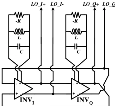
(24) reduce power consumption. However, the circuit performance degrades and one gets low circuit bandwidth and voltage swing at low voltage. Scaling down the threshold voltage of MOSFETs compensates for this performance loss to some degree, but this result in increased static power dissipation [34]. There are two receiver realized with low voltage supply for 5-GHz wireless application [35][36]. One comprising a differential LNA, an active mixer, and a quadrature voltage-controlled oscillator exhibits high linearity. The other comprising a differential LNA, a Gilbert mixer, integer-N frequency synthesizer, AGC loop, and low-pass channel-select filter performs low-power consumption.. 1.3 MOTIVATION In IEEE 802.11a, the center sub-channel is unused, providing an empty spectrum of +/- 156.25 kHz after translation to the baseband. It is very favorable for direct-conversion architecture. Base on this reason, the design of this thesis is to realize a 1-V 5-GHz direct-conversion front-end receiver based on IEEE 802.11a specification and integrated with LNA, quadrature VCO and downconverter for low-power wireless system applications by TSMC 0.18μm technology. The standard specifies an operating frequency range 5.15 ~ 5.35 GHz with 8 channels of 20 MHz bandwidth per-channel. This thesis is proposed a new offset compensation circuit with band-pass filter as the downconverter loads to suppress extraneous offset voltages corrupt the signal and saturate the following stages. Based on low-power consumption, this trend dictates that the RF front-end receiver will have to operation with low supply voltage. The receiver adopts differential circuits to reduce the even-order distortion effect, selected PMOS and provided adequate gain to minimize the flicker noise. Quadrature LC-VCO architecture is to make it less sensitive to I/Q mismatches. Fig 5 shows the receiver architecture in this thesis. - 11 -.
(25) 1.4 THESIS ORGANIZATION Chapter 2 proposes a downconverter comprising DC offset compensation circuit with design considerations, post-simulation results on downconverter. The down converter is also applied in a proposed RF receiver front-end. Chapter 3 illustrates IEEE 802.11a PHY standard and link budget of circuit block. The low-voltage RF receiver front-end comprises a differential LNA, two downconverters and a quadrature voltage-controlled oscillator. The implementation and post-simulation results is completed. Chapter 4 contains experimental results and discussions. Finally, conclusions and future works are described in Chapter 5.. Quadrature VCO CosWLOQ t. SinWLOI t. RF. Downconverter _Q path. IF Output Q_path. LNA. Downconverter _I path Fig. 5. Receiver architecture in this thesis. - 12 -. IF Output I_path.
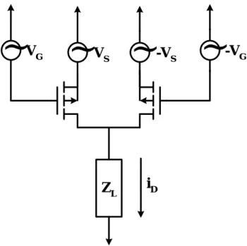
(26) CHAPTER 2 DOWNCONVERTER WITH DC OFFSET COMPENSATION. In the radio frequency transceiver operated in the gigahertz range, the quadrature modulator/de-modulator is one of the key components, which has significant effects in the quality of converted signals. The direct-conversion quadrature downconverter can effectively reduce cost, power dissipation, and chip area compared to the heterodyne quadrature modulator. It also has good performance in image rejection and LO leakage.. 2.1 OPERATIONAL PRINCIPLE Downconverters are commonly used to multiply signals of different frequencies in an effort to achieve frequency translation. Clearly a linear system cannot achieve such a task, and it need to select a nonlinear device such as a diode, BJT, or FET that can generate multiple harmonics. Consider an N-MOS device operating in saturation region. The drain current is function of the gate and source voltages, ideally written as iD = K [(vG - vS) - VT]2 = K [vG2 – 2vGvS + vS2 – 2(vG - vS) + VT2] , Where K =. (1). 1 W µ 0COX and VT are assumed to be constants. Suppose a basic cell is 2 L. designed to have an input/output relation similar to (1), shown in Fig. 6. It depicts the basic system arrangement of a mixer connected to an RF signal, a1, and local oscillator signal, b1, which is also known as the pump signal. The function is supposed to be. - 13 -.
(27) a1. X. b1. d1. Fig. 6 Basic cell X. d1 = a1 − 2 ⋅ a1b1 + b1 − 2 ⋅ (a1 − b1 ) ⋅ C + C 2 , where C is a constant. 2. 2. Next step, include another basic cell X to construct a differential-input one, basic cell Y, illustrated in Fig. 7. a1. X. b1. +. a1 b1 -a1 -b1. d2. +. -a1. Y. d2. X. -b1. Fig. 7. Basic cell Y constructed by two basic cells X The second basic cell X is fed by –a1 and –b1, then input/output relation of basic cell Y. (. ). is d 2 = 2 ⋅ a1 + b1 − 4 ⋅ a1b1 + 2 ⋅ C 2 . Fig 8 presents a double-balanced structure for 2. 2. another function, where. {[ (. ][ (. ). ). ]}. d 3 = − 2 ⋅ a1 + b1 − 4 ⋅ a1b1 + 2 ⋅ C 2 − 2 ⋅ a1 + b1 + 4 ⋅ a1b1 + 2 ⋅ C 2 = 8 ⋅ a1b1 2. 2. 2. 2. (2). In this thesis, the downconverter is used the double-balanced structure and if substitution of parameters is introduced as a1 = cos ω RF t , b1 = cos ω LO t. , the input/output relation becomes d 3 = 8 cos ω RF ⋅ t × cos ω LO ⋅ t The result can corresponds to the I-channel of quadrature IF output. By the same way, - 14 -.
(28) the Q-channel IF output is obtained if a1 = cos ω RF t , b1 = sin ω LO t. a1 b1 -a1 -b1. a1 -b1 -a1 b1. Y + -. d3. Y Fig. 8. Double-balanced structure. 2.2 DESIGN CONSIDERATION 2.2.1 DC Offset Compensation As previously chapter mention, the DC offset is generated by self-mixing effect. Generally, the total gain from the RF antenna to the ADC is typically around 100 dB so as to amplify the microvolt input signal to a level that can be digitized by a low cost, low power ADC. Of this gain, typically around 25 dB is contributed by the LNA/mixer combination and residue is provided by the automatic gain control (AGC). If an offset is obtained resulting from self-mixing and produces at the output of the downconverter is on the order of tens-milli volt. Thus, it directly amplified by the AGC; the offset voltage saturates the following circuit or downconverter itself, thereby prohibiting the amplification of the desired signal [15]. When the self-mixing is occurred, it may treat a current appearing at the output of the downconverter. These current flows into the downconverter load and bring an extra. - 15 -.
(29) voltage on the load. Fig. 9 shows a simple example for DC offset observation. Assuming the P-MOS acts as a downconverter and the RF signal and local oscillator signal have the same frequency, this plays similarly a self-mixing situation. Supposing the extra voltage at the output of downconverter is positive.. LO. LO. RF. RF. Output. Output. Vb. \. (a) (b) Fig. 9. Simple example for dc offset observation In the Fig. 9 (a), the RF signal and LO signal will downconvert to DC and a DC current flows into the resistor, therefore a extra voltage build on the output of initial bias point. Fig. 9 (b) is a P-MOS mixer with a constant biasing load, N-MOS. After mixing signal, an additional current appear and flow into N-MOS. If the N-MOS device is in saturation region and channel-length modulation is considered, the drain current is written as: I D = K (VGS − Vt ) 2 ⋅ (1 + λVDS ). (3). , where λ is channel-length modulation parameter. The VDS voltage will vary with the ID proportionally when the voltage of VGS is constant. It means that the output voltage vary with the strength of injecting power. Larger injecting power for self-mixing process will produce more unwanted current to flow into the load, further DC offset. - 16 -.
(30) voltage appear on the output node of downconverter. It influences the downconverter itself and following stage severely. Because of substrate coupling effects are always existent: coupling of the LO to the LNA and RF port of the downconverter cause static offset or LO couples to the antenna, radiates and then reflects off moving objects back to the antenna, a time varying offset is created. The undesired reaction won’t disappear and need to handle appropriately. A new method to compensate the DC offset is proposed in this thesis. As show in Fig. 10, the P-MOS also acts as the downconverter and the output voltage is feedback to bias the N-MOS load by a large feedback resistor, instead of the constant bias, Vb. When an additional current appear by self-mixing and flow into N-MOS, the VGS=VDS as the IG is zero, the equation (3) can be re-written as: I D = K (VDS − Vt ) 2 ⋅ (1 + λVDS ). (4). With the same amount of offset current, the VDS are suppressed in square degree. The tens-milli volt order of voltage mention previously by self-mixing at the output of the downconverter can be reduced to few milli volts. The offset suppressed ability of this circuit is proportional to the transconductance of the N-MOS load.. LO. RF O utput. Rm \. Fig. 10 DC offset compensation circuit - 17 -.
(31) 2.2.2 Band-Pass Filter In the conventional receiver, the downconverter always connect to a channel select filter that can filter out the unwanted band, such as harmonic signal and any interferers outside the interesting band. Since offset removal circuit would entail channel select filter filtering the baseband signal, it is important to examine the consequences of such an operation for the modulation schemes of interest. In IEEE 802.11a specification, the center subcarrier is unused, providing an empty spectrum of ± 156.25 kHz after translation to the baseband. Thus, if the lower corner frequency of the band-pass filters, fL, fall below this value, then the spectrum of the subcarriers carrying information remains intact. Consequently, a lower corner frequency of 150 kHz and bandwidth of 10 MHz band-pass filters are required. A second-order LC high-pass filter with low corner frequency (about 150 kHz) is required a very high Q value, a value difficult to achieve. It is important to note that typical filters exhibit a trade-off between the loss and the Q value. In order to significantly relax the linearity and Q value requirement of the baseband stage, the front-end receiver chain further contains a band-pass filter to provide partial channel selection.. LO. Z. RF. Rm \. Cn. Cm. Fig. 11. A band-pass filter as downconverter load - 18 -.
(32) The downconverter contains a band-pass filter showing in Fig. 11. The P-MOS also acts the downconverter and the Cm is connected at gate of the N-MOS to form a simple partial channel selection filter. Because of the N-MOS is worked in the saturation inevitably, using the small-signal model of the N-MOS device, hybrid-π model, and the output impedance looking from Z of Fig. 11 can be written as: Z=. =. ≅. 1 + Rm ⋅ (Cm + C gd )⋅ S. Cm ⋅ C gd ⋅ Rm ⋅ S + (Cm + C gd ⋅ Rm ⋅ g m )⋅ S + g m 2. ro 1 + ro ⋅ Cn ⋅ S. (5). Rm ⋅ (Cm + C gd )⋅ S + 1. Rm(Cm + C gd ) 1 Rm(CmCn + C gd Cn + CmC gd )⋅ S 2 + Cn + Cm + C gd g m Rm + ⋅ S + + gm ro ro 1 + Rm ⋅ Cm ⋅ S Cm ⋅ Cn ⋅ Rm ⋅ S 2 + (Cm + Cn ) ⋅ S + gm. , where the Cgs is lumped with Cm. ro is the MOS small-signal output resistance and gm is top-gate transconductance. From the equation (5), the output impedance Z very with frequency and it has two corner frequencies, fL and fH. The fL is mainly decided by the Cm and Rm. The fH is dominated by the Cn. Proper choosing the passive elements can get the required frequency spectrum as showing in Fig 12, if the output impedance of downconverter is greater than the load Z. Using this kind of impedance treat as downconverter load and the IF output is accomplished a simply channel selection. A new DC offset compensation circuit with band-pass filter is proposed. Without DACs or complex multi-phase architecture, this circuit uses a few passive components to achieve offset compensation and filtering and it is effective in that it does not incur any in-band loss. The proposed circuit doesn’t increase numerous power dissipations and a benefit for low-voltage and low-power design.. - 19 -.
(33) Fig. 12. Band-pass impedance frequency spectrum. 2.2.3 Voltage Conversion This subsection describes how circuit devices construct the function block and the voltage conversion in preceding discussion. Referring to Fig. 13, basic cell X in Fig. 6 is realized by a PMOS device. By the similar way, implementation of basic cell Y is presented in Fig. 14. To realize the output result in equation (2), Fig 14 is developed to Fig. 15. The equation (2) can be modified to equation (6), a more realistic function, by the circuit implementation in Fig. 15. d 3 = 8Z L K ⋅ VG ⋅ VS. ~. VG. ~. ZL. (6). VS. iD. Fig. 13. Realizations of basic cell X - 20 -.
(34) ~. VG. ~. ~. VS. -VS. ~. -VG. iD. ZL. Fig. 14. Realizations of basic cell Y. ~. VG. ~. ~. VS. ZL. -VS. ~. -VG. +. +. ~. -VG. ~. VS. ~. -VS. ~. VG. -d3. ZL. Fig. 15. Realizations of double-balanced combiner All developments for the downconverter are originally based on equation (1), ideal square- law. Because of channel pinched-off, a MOS device works in saturation region. If a short-channel device is employed in circuit implementation, another mechanism causing saturation is involved [37]. In a short-channel device, velocity saturation occurs before pinched-off. Taking velocity saturation and mobility degradation into consideration, equation (7) presents an advanced formula modified from the ideal. - 21 -.
(35) square-law, where vsat denotes saturated velocity and θ is a fitting parameter approximately equaling to. ID =. 10 −7 −1 V tox. 1 W µ 0COX ⋅ 2 L. ≈. (VGS − VT )2 µ0 1+ + θ ⋅ (VGS − VT ) 2vSAT L. W µ0 1 2 + θ ⋅ (VGS − VT ) ⋅ (VGS − VT ) µ 0COX ⋅ 1 − L 2vSAT L 2 . (7). According to equation (7), equation (6) is modified to equation (8) µ0 + θ ⋅ (VGS − VT ) ⋅ VG ⋅VS d 3 = 8Z L K 1 − 2vSAT L . (8). The result indicates that the designed downconverter performs expected function on condition that MOS devices work in saturation region with sufficiently small overdrives. For circuit implementation, the VG would be the RF signal and VS is LO signal. Generally, the load and LO signal, ZL and VS, influences the d3, output voltage amplitude directly.. 2.2.4 Noise and Linearity The single-balanced configuration exhibits less input-referred noise for a given power dissipation than the double-balanced counterpart. However, the circuit is more susceptible to noise in the LO signal. It is more intensified by the high noise floor of typical oscillators. In both mixer topologies, a differential output provides much more immunity than single-ended output to feedthrough of the RF signal to the IF output. By contrast, if the output is sensed differentially, the effect of direct feedthrough is much less significant. It implies that the differential output have better noise figure than single-ended IF output. Accordingly, a differential band-pass filter is needed; the differential output of the downconverter can directly drive the filter [4]. After downconverter, the downconverter spectrum is around zero frequency, flicker - 22 -.
(36) noise of devices has profound effect on the signal. Therefore the downconverter is the most critical stage in the receiver chain in combating the flicker noise. In most cases, the magnitude of the input-referred flicker noise component is approximately independent of bias current and voltage and is inversely proportional to the active gate area of the transistor. The latter occurs because as the transistor is made larger, a larger number of surface states are present under the gate, so that an averaging effect occurs that reduces the overall noise. It is also observed that the input-referred flicker noise is an inverse function of the gate-oxide capacitance per unit area. For a MOS transistor, the equivalent input-referred voltage noise can be written as [38] 2 Kf 2 1 1 vi + ⋅ ≈ 4kT ∆f 3 g m WLCOX f. (9). 24. K f ≈ 3 × 10 − V 2 − F. It is also interesting to note that while all of downconverter are no, the MOS switches injecting noise to the output. Employing large LO swings or decreasing the drain bias current of the MOS switch can minimize the contribution of the thermal and channel thermal noise. The trade-offs described above require a careful choice of device size and bias currents so as to minimize the overall noise figure. Since holes are less likely to be trapped, P-MOS has less flicker noise than N-MOS. In order to reduce the noise figure, the downconverter should have moderate NF and adequate conversion gain to minimize the noise. This can obtain by increased the downconverter load, as designated last subsection ZL, to increasing conversion gain. With the constant bias current, the larger load impedance causes the larger voltage drop on it, thus decreases the voltage headroom of the remaining MOSFETs and degrades the linearity of the downconverter, especially for the low-voltage design. This is a trade-offs between noise and linearity. By the way, for the intrinsic nonlinearity of the transistors,. - 23 -.
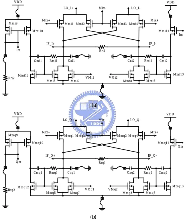
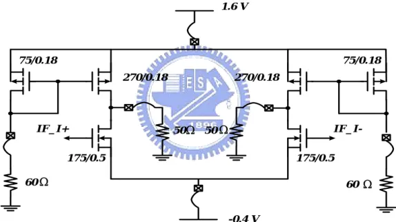
(37) it is important to notice that the distortion in inversely proportional to the gate length and this effect will become even more important when going to deeper sub-micrometer technologies [39].. 2.3 CIRCUIT REALIZATION Based on the considerations in the previous section, a downconverter with DC offset compensation circuit is designed. Fig. 16 presents downconverter divided into I/Q-channel paths and lists the relative parameter information in Table2-1. The downconverter is double-balanced counterpart and fully differential configuration. In the aspect of low-voltage design, the downconverter doesn’t use the conventional Gilbert cell. The V/I converter of Gilbert cell is removed and direct connects to designed VCO output in order to save the voltage headroom. It needs no re-bias on the source terminals. To realize the direct connection and flicker noise consideration, P-MOS devices are employed as the downconverter. Furthermore the load of downconverter is implemented with N-MOS device. Total DC-drop from sum of sufficient drain-source voltage is merely about 0.4 V by TSMC 0.18-μm technology. In the condition, downconverter function is achievable at 1-V supply voltage. Because of the corner frequency, fL as shown in Fig.12, is obtained by the Rm and Cm product approximately, Cm will occupy a large area when the resister value smaller, vice versa. In order to save the chip area, the Cm is replaced by Cmi1 and Mmi12, for example, in the Fig. 16 (a). It uses the Miller effect to multiply Cmi1. With the proper design, the Cmi1 can be multiplied about 16, saving a lot chip area. The Rm is used high resister type such as the HRI P-poly resister without silicide. The Rri1 or Rrq1 is used to make the load of downconverter more flatness in the interesting band. The differential circuit is very sensitive to device symmetrization. Using Mmq7 and Mmq8, or Mmi7 and Mmi8, with off-chip bias, the adjustable bias, VMi# and VMq#, can - 24 -.
(38) cancel the offset voltage brought by the device mismatch. It is also option to compensate the DC offset using varying bias controlled by the DACs, such as in [25], but this will make circuit more complexity. VDD. VDD L O _I+. M ix-. L O _I-. M ix+. M m i9. M ix+ M m i1 M m i2. M m i3 M m i4 M m i11. M m i10. Im IF _I-. IF _I+ Im. R ri1 Cm i1. Rm i1. M m i12. R ri2. Cni2. Cni1. V M i1 M m i5. R m i2. C m i2. M m i13. V M i2 M m i8. M m i7. M m i6. (a) VDD. VDD L O _Q +. M ix-. L O _Q -. M ix+. M m q9. M ix+ M m q1 M m q2. M m q3 M m q4 M m q11. M m q10. Qm IF _Q -. IF _Q + Qm. R rq1 C m q1. R rq2. R m q1. C nq1. M m q12. C nq2. V M q1 M m q5. M m q7. R m q2. M m q13. V M q2 M m q8. M m q6. (b) Fig. 16. (a) I-channel and (b) Q-channel of double-balanced downconverter with DC offset compensation circuit. - 25 -. C m q2.
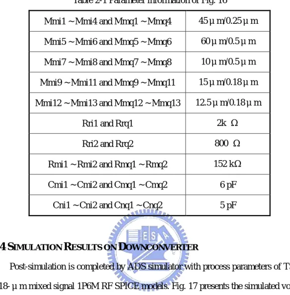
(39) Table 2-1 Parameter information of Fig. 16 Mmi1 ~ Mmi4 and Mmq1 ~ Mmq4. 45μm/0.25μm. Mmi5 ~ Mmi6 and Mmq5 ~ Mmq6. 60μm/0.5μm. Mmi7 ~ Mmi8 and Mmq7 ~ Mmq8. 10μm/0.5μm. Mmi9 ~ Mmi11 and Mmq9 ~ Mmq11. 15μm/0.18μm. Mmi12 ~ Mmi13 and Mmq12 ~ Mmq13. 12.5μm/0.18μm. Rri1 and Rrq1. 2k Ω. Rri2 and Rrq2. 800 Ω. Rmi1 ~ Rmi2 and Rmq1 ~ Rmq2. 152 kΩ. Cmi1 ~ Cmi2 and Cmq1 ~ Cmq2. 6 pF. Cni1 ~ Cni2 and Cnq1 ~ Cnq2. 5 pF. 2.4 SIMULATION RESULTS ON DOWNCONVERTER Post-simulation is completed by ADS simulator with process parameters of TSMC 0.18-μm mixed signal 1P6M RF SPICE models. Fig. 17 presents the simulated voltage conversion gain of the downconverter. The conversion gain is about 0 dB at the interesting band and the corner frequencies are at 150 KHz and 30 MHz respectively.. Fig. 17. Simulated voltage conversion gain of the downconverter. - 26 -.
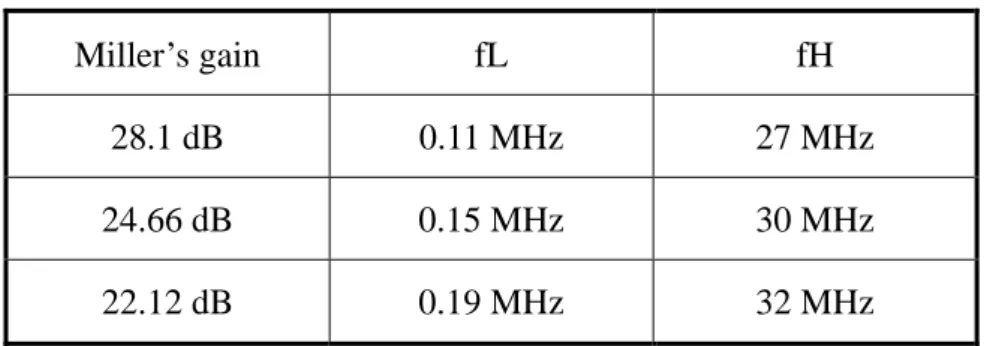
(40) The Cmi#, for example, is enlarged by Miller’s amplifier, Mmi12 and Mmi13. When the gain of the Miller’s amplifier is varied due to process variation, the corner frequency is influenced by the gain variation directly. While Miller’s amplifier is with +/- 6% dimension variations, Fig. 18 presents the each voltage gain versus frequency on gain variations and the relative corner frequency is listed in Table 2-2. The normal Miller’s gain is designed at 24.66 dB. If the dimension variation is set to +/- 3%, the fL is about 150 kHz +/- 30 kHz. Fig 19 presents output noise voltage spectral density of downconverter. The noise bandwidth of this circuit is from 150 KHz to 10 MHz and the total noise figure of the downconverter is given approximately by Nout 150 K Gain ⋅ Nin 10 M. F=∫. (10). Fig. 18 Voltage gain versus frequency on gain variations Table 2-2 Relative corner frequency of Fig.18 Miller’s gain. fL. fH. 28.1 dB. 0.11 MHz. 27 MHz. 24.66 dB. 0.15 MHz. 30 MHz. 22.12 dB. 0.19 MHz. 32 MHz. - 27 -.
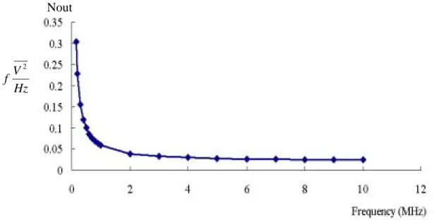
(41) Nout. f. V2 Hz. Fig. 19. Output noise voltage spectral density of downconverter , where the Nout is the output noise power, Nin is the input noise power and Gain is the voltage conversion gain of the downconverter. The noise figure of downconverter at the interesting band is 17.2dB. Two-tone test is applied to simulate linearity of the downconverter circuit. This response was obtained by feeding two signals at 5.209-GHz and 5.211-GHz to the RF port. The combined two-tone RF signal was mixed with a 0-dBm LO signal at 5.21-GHz. This setup was used to extract the 1-dB compression point and the thirdorder intercept point (IP3) by sweeping the input power level. Fig. 20 plots output power of first and third order terms relative to input power. A high input intercept of approximately 10 dBm was extrapolated, and a 1-dB compression point was observed near –0.7 dBm. Fig. 21 shows simulated results of the DC offset compensation. The RF port is fed one tone signal which frequency is same as LO frequency. After self-mixing, a signal current will appear at DC on the each output terminals of the downconverter and influence its bias level. This setup is used to estimate the circuit ability of withstand un-wanted signal leakage. By sweeping the input power level, the DC offset voltage at the differential output terminals will increase, as shown in Fig.21. The DC offset - 28 -.
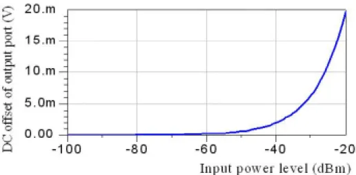
(42) voltage is about 3-mV at single output with injected power of –30-dBm and about 6-mV at differential output in same condition. The power consumption is about 1mW for the compensation circuit. At the last of chapter 2, a post-simulation summary of the downconverter is listed in Table 2-3. The power consumption shown in the table is included two paths of downconverters. The downconverters is fed with 0-dBm LO signal at 5.25-GHz and the RF port is fed with –40-dBm RF signals at 5.26-GHz during simulation.. Fig. 20. Extrapolation of downconverter IIP3. Fig. 21. DC offset voltage caused by injected leakage powers. - 29 -.
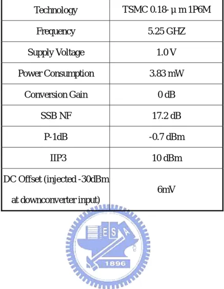
(43) Table 2-3 Post-simulation summary of the downconverter Technology. TSMC 0.18-μm 1P6M. Frequency. 5.25 GHZ. Supply Voltage. 1.0 V. Power Consumption. 3.83 mW. Conversion Gain. 0 dB. SSB NF. 17.2 dB. P-1dB. -0.7 dBm. IIP3. 10 dBm. DC Offset (injected -30dBm 6mV at downconverter input). - 30 -.
(44) CHAPTER 3 1-V 5-GHz DIRECT-CONVERSION FRONT-END RECEIVER. Direct-conversion receiver is mentioned in Chapter 1. In addition to a LNA and downconverters, the designed receiver requires a quadrature VCO. Fig. 22 gives an illustration with a block diagram. The downconverters are implemented to a double-balanced downconverter as chapter 2 mentioned. The LNA is fully differential with common-source-cascode architecture. The quadrature VCO generates quadrature LO signal and quadrature IF signal comes from downconverter of the RF and LO signals. The output buffer is used for measurement.. Quadrature VCO SinWLOI t. CosWLOQ t. Downconverter _Q path. RF. IF Output Q_path. Buffer. LNA. Downconverter _I path. Fig. 22 Block diagram of direct-conversion receiver. - 31 -. IF Output I_path.
(45) 3.1 IEEE 802.11A PHY STANDARD AND LINK BUDGET The IEEE 802.11a standard specifies over a generous 300-MHz allocation of spectrum for unlicensed operation in the 5-GHz block. Of that 300-MHz allowance, there is a contiguous 200-MHz portion extending from 5.15 to 5.35 GHz, and a separate 100-MHz segment from 5.725 to 5.825 GHz. It incorporates orthogonal frequency division multiplexing (OFDM) modulation, a technique that uses multiple carriers to mitigate the effect of multipath. IEEE 802.11a standard provides for OFDM with 52 subcarriers in a 16.6-MHz bandwidth (channel spacing of 20-MHz), 48 subcarriers are for data, the rest are for pilot signals. Each of the subcarriers can be either a BPSK, QPSK, 16-QAM, or 64-QAM signals. It provides nearly five times the data rate and as much as ten times the overall system capacity as currently available 802.11b wireless LAN systems. Information data rates of 6~54 Mb/s are supported. The standard further requires a maximum transmit constellation error at –25dB for 64-QAM modulated OFDM signal, whereas the output power cannot exceed 40 mW for channels from 5.15 to 5.25 GHz or 200 mW for channels from 5.25 to 5.35 GHz. Fig. 23 shows a lower frequency band of the channel allocation [40]. 200 m W 40 m W. 5.15 G. 5.25 G. 5.35 G. 20 M H z fo +312.5 K. fo. fo +187.5 K. 20 M H z with 52 carriers. Fig. 23 IEEE 802.11a lower frequency band of the channel allocation - 32 -.
(46) The spectral efficiency of 802.11a standard comes at the expense of a more complicated receiver with strict requirements on the radio performance. For example, the use of 64-QAM modulation requires a signal-to-noise ratio (SNR) of 30 dB, which is substantially greater than required by the FSK modulation in Bluetooth and the QPSK modulation in 802.11b. This high SNR translates to tight I/Q matching constraints for the receiver. It also results in the stringent demands for the performances of both noise figure and image rejection. To determine the precise target value, the specification set to frequency range, noise figure, maximum input signal level or input-referred 1-dB compression point. For frequency range, it is often acceptable to cover only the lower 200-MHz band. The upper 100-MHz domain is not contiguous with that allocation, so its coverage would complicate somewhat the design of the synthesizer. Furthermore, that upper 100-MHZ spectrum is not universally available, such as HIPERLAN. Hence the choice here is to span 5.15~5.35GHz. The specification simply recommends a noise figure of 10dB, with a 5-dB implementation margin, to accommodate the worst-case situation. A 10-dB maximum noise figure is the design goal for the thesis. The standard also specifies a value of –30 dBm as maximum input signal that a receiver must accommodate (for a 10% packet error rate). Converting this specification into a precise IIP3 target or 1-dB compression requirement is nontrivial. However, as a conservative rule of thumb, the 1-dB compression point of receiver should be about 4 dB above the maximum input signal power level that must be tolerated successfully. Based on this approximation, the target of worst-case input-referred 1-dB compression point is to set at –26 dBm [41]. The IEEE 802.11a specification for this thesis required is listed in the Table 3-1. Therefore, the link budget of each circuit can be calculated by the following equation. For the noise figure of cascaded stages, the total NF can be written as. - 33 -.
(47) NFtot = NF1 +. NF2 − 1 NFm − 1 + ...... + Ap1 Ap1 Λ Ap ( m−1). (11). , where NFm express the noise and Apm express the gain of each stage. For the linearity of a general expression for cascaded stages 1 A2 IP 3. ≈. 1 A2 IP 3,1. A A ⋅A + 2 P1 + P1 2 P 2 + Λ A IP 3, 2 A IP 3,3 2. 2. 2. (12). , where AIP3,m denotes the input IP3 and Apm denotes the fundamental gain of each stage. It is also instructive to find the relationship between the 1-dB compression point and the input IP3 for a third-order nonlinearity, which the two can be related by. A1−dB ≈ −9.6dB AIP 3 Based on the analysis previously, the design target of the front-end receiver and its each circuit is listed in Table 3-2. The buffer will be used behind the downconverter for measurement. According to (11) and (12), the design target of receiver is decayed by the buffer for cascaded stages. The Table 3-2 list design target without buffer erosion. Table 3-1 IEEE 802.11a specification for this thesis required Frequency bands. 5.15 ~ 5.35 GHz. Max RX input power. -30 dBm. Noise Figure. < 15 dB. P-1dB. > -26 dBm. Channel numbers. 8. Channel bandwidth. 20 MHz. - 34 -.
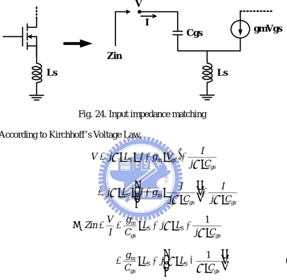
(48) Table 3-2 Design target of the front-end receiver and each circuit VDD. 1V. Gain. 23 dB. Front-End. NF. < 10 dB. Receiver. P-1dB. > -26 dBm. DC offset. < 10 mV. Power. < 25 mW. Gain. 23 dB. NF. 2 dB. P-1dB. -14 dBm. Gain. 0 dB. NF. 17.7 dB. P-1dB. 0 dBm. Tuning range. 5.15 ~ 5.35 GHz. LNA. Downconverter. Quadrature VCO. 3.2 CIRCUIT REALIZATION 3.2.1 Differential Low Noise Amplifier In RF system, the LNA, one of front-end circuits, locates on the receiving path of transceiver. The main functions are amplifying RF signal received from the antenna, providing input impedance matching and contributing as minimal noise as possible for the system working well. Input matching is an important consideration for connection with external components. Described by microwave theoretic, signal is partially reflected if passing through the interface between two different mediums. The meaning in circuit design is unequal input/output impedances between two stages. To minimize the reflection, input. - 35 -.
數據
+7
相關文件
Salmon, Automatic Creation of Object Hierarchies for Ray Tracing IEEE CG&A 1987 Object Hierarchies for Ray Tracing, IEEE CG&A, 1987. • Brian Smits, Efficiency Issues
首先,在前言對於為什麼要進行此項研究,動機為何?製程的選擇是基於
The major testing circuit is for RF transceiver basic testing items, especially for 802.11b/g/n EVM test method implement on ATE.. The ATE testing is different from general purpose
“IEEE P1451.2 D2.01 IEEE Draft Standard for A Smart Transducer Interface for Sensors and Actuators - Transducer to Microprocessor Communication Protocols
傳統的 RF front-end 常定義在高頻無線通訊的接收端電路,例如類比 式 AM/FM 通訊、微波通訊等。射頻(Radio frequency,
Park, “A miniature UWB planar monopole antenna with 5-GHz band-rejection filter and the time-domain characteristics,” IEEE Trans. Antennas
F., “A neural network structure for vector quantizers”, IEEE International Sympoisum, Vol. et al., “Error surfaces for multi-layer perceptrons”, IEEE Transactions on
LAN MAN Standards Committee of the IEEE Computer Society(1999), “ Wireless LAN Medium Access Control(MAC) and Physical Layer(PHY) Specifications,” International Standard ISO/IEC
