行政院國家科學委員會專題研究計畫 成果報告
過渡性金屬氧化物及硫屬化合物之製備,特性研究及其可能 應用之探討(3/3)
計畫類別: 個別型計畫
計畫編號: NSC93-2112-M-011-001-
執行期間: 93 年 08 月 01 日至 94 年 10 月 31 日 執行單位: 國立臺灣科技大學電子工程系
計畫主持人: 黃鶯聲
計畫參與人員: 陳自雄、黃鵬仁、劉;彥棠、張弘民、蔡宗穎、陳麒安
報告類型: 完整報告
報告附件: 出席國際會議研究心得報告及發表論文 處理方式: 本計畫可公開查詢
中 華 民 國 94 年 8 月 3 日
行政院國家科學委員會補助專題研究計畫 ■ 成 果 報 告
□ 期中進度報告
過渡性金屬氧化物及硫屬化合物之製備、特性研究 及其可能應用之探討
Growth, Characterization and Applications of Transition Metal Dioxide and Dichalcogenide Compounds
計 畫 類 別 : ■ 個 別 型 計 畫 □ 整 合 型 計 畫 計 畫 編 號 : NSC 93 - 2112 - M - 011 - 001 執行期間: 93 年 8 月 1 日 至 94 年 10 月 31 日
計 畫 主 持 人 : 黃 鶯 聲
計畫參與人員:陳自雄、黃鵬仁
國立台灣科技大學電子工程所博士班研究生 劉彥棠
國立台灣科技大學電子工程所碩士班研究生 張弘民、蔡宗穎
國立台灣科技大學工程技術所碩士班研究生 陳麒安
北台科學技術學院機電整合所碩士班研究生
成果報告類型(依經費核定清單規定繳交):□精簡報告 ■完整報告 本成果報告包括以下應繳交之附件:
□赴國外出差或研習心得報告一份
■出席國際學術會議心得報告及發表之論文各一份
處理方式:除產學合作研究計畫、提升產業技術及人才培育研究計畫、列管計畫 及下列情形者外,得立即公開查詢
□涉及專利或其他智慧財產權,□一年□二年後可公開查詢
執行單位:國立台灣科技大學電子工程所
中 華 民 國 94 年 7 月 30 日
I
一、中文摘要
本計畫目的在從事過渡金屬硫屬化合物單晶以及過渡金屬氧化物單晶與薄膜的製 備,特性研究及其可能應用之探討。具層狀結構的金屬硫合物(ReS2, ReSe2, MoS2, MoSe2, WS2, WSe2)單晶與傳統塊狀金屬氧化物(RuO2, IrO2, OsO2)單晶皆採用化學汽 相傳輸方式成長。金屬氧化物(RuO2, IrO2, OsO2)薄膜的製備乃使用應用性較高的有機金 屬化學汽相沈積法。在樣品特性量測方面,各種調制反射光譜技術將運用於研究金屬硫 合物之能帶結構與載子躍遷情形。利用X光繞射與拉曼散射實驗,可檢測單晶或薄膜樣 品之結構特性與結晶品質。利用X 光繞射與拉曼散射實驗,可檢測單晶或薄膜樣品之結構特 性與結晶品質。掃瞄式與穿透式電子顯微鏡影像用以觀察薄膜與奈米材料表面形貌與微結構特 性。
關鍵詞:過 渡 金 屬 硫 屬 化 合 物 、過 渡 金 屬 氧 化 物 、單晶、薄膜、奈米柱、化學汽相傳輸 法、有機金屬化學汽相 沈積法 、調制反射式光譜、X 光繞射、X 光光電子發射譜、拉曼散 射、掃瞄式電子顯微鏡
Abstract
Using chemical vapor transport (CVT) and metalorganic chemical vapor deposition (MOCVD) methods, We have grown transition metal dichaclogenides (ReS2, ReSe2, MoS2, MoSe2, WS2, WSe2) and transition metal dioxides (RuO2, IrO2, OsO2)with pyrite, layered or rutile structure. A detailed characterization for the single crystal or thin film samples have been carried out. Various modulation spectroscopy techniques are utilized to investigate the band structure and carrier transition for the as-grown layered semiconductor of metal dichaclogenides. Structural properties and
crystallized quality are examined using X-ray diffraction and Raman scattering method. Structural properties and crystallized quality are examined using X-ray diffraction and Raman scattering method.
Surface morphology and microstructure of the samples are observed by scanning and transmission electron microscopy.
Keywords : Transition Metal Dichaclogenide, Transition Metal Oxide, Single Crystal, Thin Film,
Chemical Vapor Transport, Metalorganic Chemical Vapor Deposition, Modulation Spectroscpoy, X- Ray Diffraction, Raman Scattering, X-Ray Photoelectron Spectroscopy, Scanning Electron Microscpopy二、計畫緣由與目的
近幾年來,過渡金屬硫屬化合物在光電化學及能源工業應用方面,頗受重視。其中MoS2
的用途甚廣,因其本身質軟,潤滑性佳,對高溫高壓的穩定性好,是其他潤滑劑所無法比擬 的。而用於碳氫化合物中,則是加氫、去氫的良好催化劑。近年來更被用為作石油中加氫去 硫的主要觸媒。而在照光後產生d-d 能帶間的轉換,不須破壞化學鍵,即不產生光腐蝕的現 象,可作為光電化學太陽電池的理想電極。RuO2,IrO2與OsO2雖為氧化物,但具有金屬般的 導電性,是近來廣受注目的新興電極材料,在光電化學及能源工業應用方面,也頗受重視。
應用上尚有以 RuO2 與CdS 組成蕭特基界面應用於積體光學,與玻璃混合燒結製成厚膜電阻,
利用RuO2薄膜作為VLSI中阻擋鋁擴散之屏障,利用 RuO2 薄膜與 SrTiO3 製作高效率的 DRAM。
II
三、研究方法及計畫成果
研究方法
1.利用化學汽相傳輸法成長ReS2, ReSe2, MoS2, MoSe2, WS2, WSe2層狀結構單晶。
2.利用化學汽相傳輸法成長RuO2, IrO2, OsO2單晶。
3.利用有機金屬化學汽相沈積法成長RuO2, IrO2, OsO2薄膜。
4.利用壓電調制反射式光譜探討層狀單晶之半導體特性。
5.利用不同方向偏極光的拉曼散射實驗探討OsO2單晶內的光子聲子交互作用以及找尋可能的
拉曼訊號位置,以期建立此種罕見的氧化物單晶之拉曼散射數據。
6.利用X光繞射與拉曼散射實驗檢測RuO2, IrO2, OsO2多晶薄膜之結構特性及結晶相變化。
7.利用掃瞄式電子顯微鏡檢視RuO2, IrO2, OsO2薄膜之表面結晶狀況。
8. 利用X光光電子發射譜檢測RuO2, IrO2, OsO2單晶與多晶薄膜之成分與固態鍵結狀態。
9. 利用穿透式電子顯微鏡檢視RuO2 與IrO2 一維奈米材料之微結構。
四、結果與討論
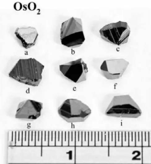
利用化學汽相傳輸法已成功地成長出大尺寸且具有清晰刻面的OsO2單晶。利用X-ray粉晶
繞射實驗,可定義出金紅石結構的OsO2晶體具有的所有可能繞射訊號位置及相對強度。於X-
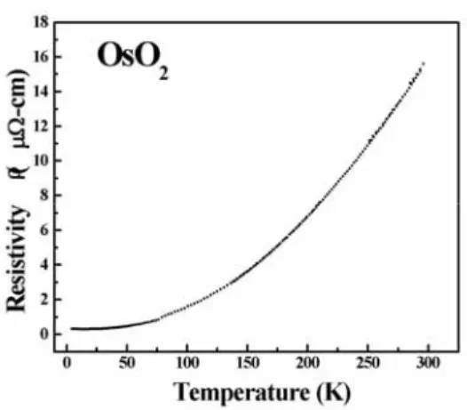
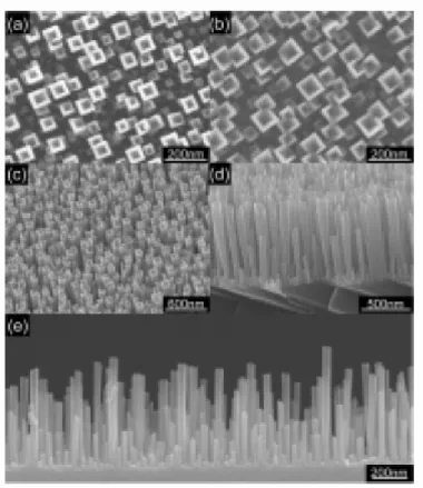
ray 光電子發射譜,亦指出OsO2單晶內所有對應Os及O原子之內層電子鍵結能位置。OsO2單晶 所量得之最低室溫電阻率約為15 µΩ-cm。另一方面,利用有機金屬化學汽相沈積法,將系統壓 力控制於1至50 Torr的範圍內,實驗上亦成功地成長出IrO2多晶薄膜及具有(002)成長方向之IrO2 奈米柱。此類氧化物之成長特性與可能機制,亦有深入的探討。透過X-ray繞射與光電子發射
譜,拉曼光譜,掃描式與穿透式電子顯微鏡,電阻率以及場發射的量測,IrO2薄膜與奈米柱之
結構,化學組成,結晶形貌以及電特性等資訊,皆能有效且深入地加以探討。利用有機金屬化
學汽相沈積法,實驗上已成功地成長出具有(001)長軸方向之IrO2 奈米柱與奈米管。利用
sapphire(100)與LiNbO3(100)基板,IrO2 奈米管可垂直成長於基板上。利用sapphire(100)與 LiNbO3(100)基板,IrO2 奈米管可垂直成長於基板上。利用LiTaO3(012)基板,IrO2 奈米管會以 單一且一致的35°傾斜角成長於基板上。對於這種具有明顯基板效應的成長結果,透過X-ray 繞 射,掃描式與穿透式電子顯微鏡的量測,我們可詳細地對此類效應有明確的瞭解與提出適當的 解釋。
五、參考文獻
1. D. B. Rogers, R. D. Shannon, A. W. Sleight and J. L. Gillson, Inorg. Chem. 8 (1969) 841.
2. D. D. Sarma and C. N. R. Rao, J. Electron Spectrosc. Relat. Phenom. 20 (1980) 25.
3. B. R. Chalamala, Y. Wei, R. H. Reuss, S. Aggarwal, B. E. Gnade, R. Ramesh, J. M. Bernhard, E.
D. Sosa, D. E. Golden, Appl. Phys. Lett. 74 (1999) 1394.
4. M. H. Huang, S. Mao, H. Feick, H. Yan, Y. Wu, H. Kind, E. Weber, R. Russo, Y. Yang, Science 292 (2001) 1897.
研究計畫相關成果:
1. Hsieh, C. S., G. Wang, D. S. Tsai, R. S. Chen, and Y. S. Huang, “Field emission characteristics of ruthenium dioxide nanorods, Nanotechnology, Accepted (2005)
2. Wu, C. C., C. H. Ho, J. Y. Wu, S. L. Lin, and Y. S. Huang, “Characterization of Ge(Se1-xSx)2
series layered crystals grown by vertical Bridgman method,” J. Crys. Growth, Accepted (2005).
III
3. Hu, S. Y., M. C. Cheng, K. K. Tiong, and Y. S. Huang, “The electrical and optical anisotropy of rhenium-doped WSe2 single crystals,” J. Physics: Conden. Matter, Vol. 17, pp. 3575-3583 (2005).
4. Ke, Y. F., D. S. Tsai, and Y. S. Huang, “Electrochemical capacitors of RuO2 nanophase grown on LiNbO3(100) and Sapphire (0001) substrates,” J. Mater. Chem., Vol. 15 pp. 2122-2127 (2005).
5. Cheng, C. L., Y. F. Chen, R. S. Chen and Y. S. Huang, “Raman scattering and field emission properties of RuO2 nanorods,” Appl. Phys. Lett., Vol.86, pp.103104-1~103104-3 (2005).
6. Chen, R. S., H. M. Chang, Y. S. Huang, D. S. Tsai, and K. C. Chiu, “Morphological evolution of the self-assembled IrO2 one-dimensional nanocrystals,” Nanotechnology, Vol. 16, pp. 93-97 (2005)
7. Wang, G., C. S. Hsieh, D. S. Tsai, R. S. Chen, and Y. S. Huang, “Area-selective growth of
ruthenium dioxide nanorods on LiNbO3(100) and ZnO/Si substrates,” J. Mater. Chem., Vol. 14 pp.
3503-3508 (2004)
8. Chen, C. C., R. S. Chen, T. Y. Tsai, Y. S. Huang, D. S. Tsai and K. K. Tiong, “The growth and characterization of well aligned RuO2 nanorods on sapphire substrates,” J. Physics: Conden.
Matter, Vol.16, pp. 8475-8484 (2004)
9. Hsieh, C. S., D. S. Tsai, R. S. Chen, and Y. S. Huang, “Preparation of ruthenium dioxide
nanorods and their field emission characteristics,” Appl. Phys. Lett., Vol. 85, pp. 3860-3812 (2004) 10. Lin, J. J., S. M. Huang, Y. H. Lin, T. C. Lee, H. Liu, X. X. Zhang, R. S. Chen, and Y. S. Huang,
“Low temperature electrical transport properties of RuO2 and IrO2 single crystals,” J. Physics:
Conden. Matter, Vol.16, pp. 8035-8041 (2004).
11. Chen, R. S., Y. S. Huang, Y. M. Liang, D. S. Tsai and K. K. Tiong, “Growth and characterization of iridium dioxide nanorods,” J. Alloys and Compounds , Vol. 383, pp. 273-276 (2004)
12. Yen, P. C., R. S. Chen, C. C. Chen, Y. S. Huang, K. K. Tiong, and P. C. Liao, “Preparation and characterization of OsO2,” J. Alloys and Compounds, Vol. 383, pp. 277-280 (2004)
13. Hu, S. Y., S. C. Lin, K. K. Tiong, P. C. Yen, Y. S. Huang, C. H. Ho and P. C. Liao, “Growth and characterization of tungsten and molybdenum-doped ReSe2 single crystals,” J. Alloys and
Compounds, Vol. 383, pp. 63-68 (2004)
14. Wu, C. C., C. H. Ho, W. T. Shen, Z. H. Cheng, Y. S. Huang, and K. K. Tiong, “Optical properties of GaSe1-xSx series layered semiconductors grown th vertical Bridgman method,” Materials
Chemistry and Physics, Vol. 88, pp. 313-317 (2004).
15. Yen, P. C., H. P. Hsu, Y. T. Liu Y. S. Huang and K. K. Tiong,” Temperature dependent study of energies and broadening parameters of the band-edge excitons of Re-doped WS2 and 2H-WS2 single crystals,” J. Physics: Conden. Matter, Vol. 16, pp. 6995-7005 (2004).
16. Chen, R. S., C. C. Chen, Y. S. Huang, C. T. Chia, H. P. Chen, D. S. Tsai, K. K. Tiong, “A comparative study of microstructure of RuO2 nanorods via Raman scattering and field emission scanning electron microscopy,” Solid State Communications, Vol. 131, pp. 349-353 (2004).
17. Chen, R. S., Y. S. Huang, D. S. Tsai, S. Chattopadhyay, C. T. Wu, Z. H. Lan and K. H. Chen,
“Growth of well aligned IrO2 nanotubes on LiTaO3(012) substrate,” Chemistry of Materials, Vol.
16, pp. 2457-2462 (2004).
18. Yen, P. C., Y. S. Huang and K. K. Tiong, “Growth and characterization of rhenium-doped WS2
single crystals,” J. Physics: Conden. Matter, Vol. 16, pp. 2171-2180 (2004).
19. Chen, R. S., Y. S. Huang, Y. M. Liang, C. S. Hsieh, D. S. Tsai and K. K. Tiong, “Field emission from conductive vertically aligned IrO2 nanorods,” Appl. Phys. Lett., Vol. 84, pp. 1552-1554 (2004).
20. Yen, P. C., R. S. Chen, C. C. Chen, Y. S. Huang, and K. K. Tiong, “Growth and characterization of OsO2 single crystals,” J. Crystal Growth, Vol. 262, pp. 271-276 (2004).
21. Chen, R. S., Y. S. Chen, Y. S. Huang, Y. L. Chen. Y. Chi, C. S. Liu, K. K. Tiong, and A. J. Carty,
“Growth of IrO2 films and nanorods by means of chemical vapor deposition: An example of compositional and morphological control of nanostructures,” Chemical Vapor Deposition, Vol. 9, pp. 301-305 (2003).
22. Chen, R. S., Y. S. Huang, Y. M. Liang, D. S. Tsai, Y. Chi, and J. J. Kai, “Growth control and characterization of vertically aligned IrO2 nanorods, “ J. Mater. Chem., Vol. 13, pp. 2525-2529
IV
(2003).
23. Song, Y. H., Y. L. Chen, Y. Chi, C. S. Liu, W. L. Ching, R. S. Chen, Y. S. Huang, and A. J.
Carty, “Deposition of conductive Ru and RuO2 thin films employing pyrazolate complex
[Ru(CO)3(3,5-(CF3)2-pz)2 as CVD source reagent,”, Chemical Vapor Deposition, Vol. 9, pp. 162- 169 (2003).
24. Yen, P. C., R. S. Chen, Y. S. Huang, C. T. Chia, R. H. Chen, and K. K. Tiong, “The first-order Raman spectra of OsO2,” J. Phys.: Condens. Matter, Vol. 15, pp. 1487-1494 (2003).
25. Ho, C. H., P. C. Yen, Y. S. Huang, and K. K. Tiong, “Photoreflectance study of the excitonic transitions of rhenium disulphide layer compounds,” Phys. Rev. B, Vol. 66, pp. 245207- 1~245207-5 (2002).
26. Chen, R. S., Y. S. Huang, Y. L. Chen, and Y. Chi, “Preparation and characterization of RuO2 thin films from Ru(CO)2(tmhd)2 by metalorganic chemical vapor deposition,” Thin Solid Films, Vol.
413, pp. 85-91 (2002).
27. Yen, P. C., M. J. Chen, Y. S. Huang, C. H. Ho, and K. K. Tiong, “Preparation and
characterization of molybdenum-doped ReS2 single crystals,” J. Phys.: Condens. Matter, Vol. 14, pp.4737-4746 (2002).
五、計畫成果自評
在此三年中,除實驗室本身發表上述研究成果之外也與其它研究團對合作,總共發表與計劃相 關論文 27 篇,成果豐碩。
Figure 1. Some representative crystals of OsO2 grown by chemical vapor transport method in our laboratory.
V
Figure 2. X-ray diffraction pattern of OsO2.
Figure 3. The temperature dependence of the resistivity in the range of 4.2 to 300 K for OsO2 singlecrystal.
VI
Figure 4. (a) The XPS spectrum of OsO2 single crystal. (b) Os 4f and 5p spectrum of OsO2 (solid line). The dot line shows the fitted 4f7/2 and 4f5/2 doublet components and 5p3/2 feature. (c) O1s spectrum of OsO2 (solid line) and the fitted curve (dot line).
Fig.5. FESEM images of the IrO2 nanorods grown on the Ti-coated-Si substrate: (a) top view; (b) 45° cross sectional view;
(c) and (d) views of the nanorod with larger spiral-shaped tip.
VII
Fig.6. (a) The schematic diagram of a typical IrO2 nanorod. (b) TEM image focused on the tip of a nanorod and (c) its corresponding electron diffraction pattern taken along [010] zone axis.
VIII
Fig. 7. FESEM images of the vertically aligned IrO2 nanotubes grown on the sapphire(100) substrate. (a) and (b) top view;
(c) perspective view; (d) and (e)cross view.
Fig. 8. TEM images of the IrO2 nanotubes focused on (a) two individual tubes; (b) the front end; (c) the middle; (d) the bottom. (e) The high-resolution TEM image and its SAD pattern taken from the tube-wall in 5.3(b). (f) A schematic diagram of the IrO2 nanotube.
IX
Fig. 9. FESEM images of the well aligned IrO2 nanotubes grown on LiTaO3 (012) substrate. (a) and (b) top view; (c) cross view; (d) focus on a typical IrO2 nanotube.
Fig.10. TEM images of the IrO2 nanotubes focused on (a) two individual tubes; (b) the front end; (c) the middle; (d) the bottom. (e) The high-resolution TEM image and its SAD pattern taken from the tube-wall in 5.3(b). (f) A schematic diagram of the IrO2 nanotube.
X
Fig.11. FESEM images of the well aligned IrO2 nanotubes grown on LiTaO3 (012) substrate. (a) and (b) top view; (c) cross view; (d) focus on a typical IrO2 nanotube.
Fig.12. (a) The cross-sectional TEM image of the IrO2 nanotubes on LiTaO3 (012) substrate, and its corresponding SAD patterns taken separately from the regions of (b) IrO2 nanotubes, (c) LiTaO3 substrate and (d) interface along the zone axes of IrO2 ] [ 11 1 and LiTaO3 ] [ 1 2 2 . (e) The schematic diagram of the orientation relationship between the nanotube and substerate.
XI
Fig.13. The top- and 30◦ perspective-viewFESEM micrographs and the corresponding schematic plots for (a)–(c) the incomplete nanotubes and (d)–(f) the scrolled nanotubes of IrO2.
Fig. 14. (a) The morphology distribution of various IrO2 1D nanocrystals in terms of supersaturation degree _μ and substrate temperature Ts. (b) The schematic diagram showing the trend of the morphological evolution of IrO2 in terms of _μ and 1/Ts. Here, 3D means the individual crystallite performing isotropic 3D growth.
XII
Fig.15. X-ray diffraction patterns of the Re-doped WS2 with x = 0.5%, 1% and undoped WS2. The additional lines (marked by *) were attributed to the presence of the rhombohedral polytype (3R).
Fig.16. The temperature dependent conductivity σ in the range of 10 to 500 K for the W1-xRexS2 single crystals. The slopes of ln⌠ versus 1000/T yield carrier activation energies for the samples.
XIII
Fig.17. The variation of the absorption coefficient for the W1-xRexS2 single crystals with photon energy.
Fig.18. The experimental points of ( 〈h ⎨)1/2, deduced from absorption measurements, versus photon energy for the W1-
xRexS2 single crystals. The solid curves are the leastsquares fits to equation (3).
XIV
Fig19. The PzR spectra of the W1-xRexS2 single crystals at 300 K. The solid curves are the least-squares fits using equation (4). Arrows under the curves show the peak positions of the two interband excitonic features, A and B, respectively. The antiresonance feature denoted AR for WS2 is also indicated.
XV