行政院國家科學委員會專題研究計畫 期中進度報告
過渡性金屬氧化物及硫屬化合物之製備,特性研究及其可能 應用之探討(1/3)
計畫類別: 個別型計畫
計畫編號: NSC91-2112-M-011-001-
執行期間: 91 年 08 月 01 日至 92 年 07 月 31 日 執行單位: 國立臺灣科技大學電子工程系
計畫主持人: 黃鶯聲
計畫參與人員: 陳自雄、嚴本嘉、陳瑞山、霍克孝、周裕煥、吳政恩、李國豪
報告類型: 精簡報告
報告附件: 出席國際會議研究心得報告及發表論文 處理方式: 本計畫可公開查詢
中 華 民 國 92 年 6 月 6 日
行政院國家科學委員會專題研究計畫期中精簡報告
過渡性金屬氧化物及硫屬化合物之製備、特性研究及其可能應用之探
討
Growth, Characterization and Applications of Transition Metal Dioxide and Dichalcogenide Compounds
計劃編號:NSC91-2112-M-011-001 執行期限:91 年 8 月 1 日至 92 年 7 月 31 日 主持人:黃鶯聲 國立台灣科技大學電子工程系 計畫參與人員:陳自雄、嚴本嘉、陳瑞山、
霍克孝、周 裕煥、吳政恩、
李國豪
一、中文摘要
本計畫目的在從事過 渡 金 屬 硫 屬 化 合 物 單 晶 以 及 過 渡 金 屬 氧 化 物 單 晶 與 薄 膜 的 製 備 , 特 性 研 究 及 其 可 能 應 用 之 探 討 。 具 層 狀 結 構 的 金 屬 硫 合 物 (ReS2, ReSe2, Mo S2, Mo Se2, WS2, WSe2)單 晶 與 傳 統 塊 狀 金 屬 氧 化 物 (RuO2, IrO2, OsO2)單 晶 皆 採 用 化學汽相傳輸方式成長。金 屬 氧 化 物 (RuO2, IrO2, OsO2)薄 膜 的 製 備 乃 使 用 應 用 性 較 高 的 有 機 金 屬 化 學 汽 相 沈 積 法 。 在 樣 品 特 性 量 測 方 面 , 各 種 調 制 反 射 光 譜 技 術 將 運 用 於 研 究 金 屬 硫 合 物 之 能 帶 結 構 與 載 子 躍 遷 情 形 。 利 用 X 光 繞 射 與 拉 曼 散 射 實 驗 , 可 檢 測 單 晶 或 薄 膜 樣 品 之 結 構 特 性 與 結 晶 品 質 。 X 光 光 電 子 發 射 譜 則 用 於 量 測 樣 品 的 成 分 與 鍵 結 狀 態 。 掃 瞄 式 電 子 顯 微 鏡 影 像 用 以 觀 察 薄 膜 表 面 結 晶 狀 況 與 換 算 薄 膜 沈 積 速 率 。
關鍵詞:過 渡 金 屬 硫 屬 化 合 物 、過 渡 金 屬 氧 化 物 、單晶、薄膜、奈米柱、化 學汽相傳輸法、有 機 金 屬 化 學 汽 相 沈 積 法 、調制反射式光譜、X 光繞射、X 光 光電子發射譜、拉曼散射、掃 瞄 式 電 子 顯 微 鏡
Abstract
Using chemical vapor transport (CVT) and metalorganic chemical vapor deposition (MOCVD) methods, We have grown transition metal dichaclogenides (ReS2, ReSe2, Mo S2, Mo Se2, WS2, WSe2) 廣受注目的新興電極材料,在光電化學及 能源工業應用方面,也頗受重視。應用上 尚有以 RuO2 與 CdS 組成蕭特基界面應 用於積體光學,與玻璃混合燒結製成厚膜
and transition metal dioxides (RuO2, IrO2, OsO2)with pyrite, layered or rutile structure. A detailed characterization for the single crystal or thin film samples have been carried out. Various modulation spectroscopy techniques are utilized to investigate the band structure and carrier transition for the as-grown layered semiconductor of metal dichaclogenides.
Structural properties and crystallized quality are examined using X-ray diffraction and Raman scattering method. Chemical compositions and binding states of as-grown samples are measured using X-ray photoelectron spectroscopy. Surface morphology and film thickness for the samples is observed by scanning electron microscopy.
Keywords : Transition Metal Dichaclogenide, Transition Metal Oxide, Single Crystal, Thin Film, Chemical Vapor Transport, Metalorganic Chemical Vapor Deposition, Modulation Spectroscpoy, X-Ray Diffraction, Raman Scattering, X-Ray Photoelectron Spectroscopy, Scanning Electron Microscpopy
二、計畫緣由與目的
近幾年來,過渡金屬硫屬化合物在光 電化學及能源工業應用方面,頗受重視。其 中 MoS2的用途甚廣,因其本身質軟,潤滑性 佳,對高溫高壓的穩定性好,是其他潤滑劑 所無法比擬的。而用於碳氫化合物中,則是 加氫、去氫的良好催化劑。近年來更被用為 作石油中加氫去硫的主要觸媒。而在照光後 產生 d-d 能帶間的轉換,不須破壞化學鍵,
即不產生光腐蝕的現象,可作為光電化學太 陽電池的理想電極。RuO2,IrO2與 OsO2雖為 氧化物,但具有金屬般的導電性,是近來
電阻,利用 RuO2薄膜作為 VLSI 中阻擋鋁 擴散之屏障,利用 RuO2 薄膜與 SrTiO3
製作高效率的 DRAM。
三、研究方法及計畫成果
研究方法
1. 利 用 化 學 汽 相 傳 輸 法 成 長 ReS2, ReSe2, Mo S2, Mo Se2, WS2, WSe2層 狀結構單晶。
2.利用化學汽相傳輸法成長 RuO2, IrO2, OsO2單晶。
3. 利 用 有 機 金 屬 化 學 汽 相 沈 積 法 成 長 RuO2, IrO2, OsO2 薄膜。
4.利用壓電調制反射式光譜探討層狀單晶 之半導體特性。
5.利用不同方向偏極光的拉曼散射實驗探 討 OsO2單晶內的光子聲子交互作用以 及找尋可能的拉曼訊號位置,以期建立 此種罕見的氧化物單晶之拉曼散射數 據。
6. 利 用 X 光 繞 射 與 拉 曼 散 射 實 驗 檢 測 RuO2, IrO2, OsO2多晶薄膜之結構特 性及結晶相變化。
7. 利 用 掃 瞄 式 電 子 顯 微 鏡 檢 視 RuO2, IrO2, OsO2薄膜之表面結晶狀況。
8. 利用 X 光光電子發射譜檢測 RuO2, IrO2, OsO2 單晶與多晶薄膜之成分與 固態鍵結狀態。
計畫成果:
1. P. C. Yen, R. S. Chen, Y. S. Huang, C. T.
Chia, R. H. Chen and K. K. Tiong, “The First-Order Raman Spectra of OsO2”, J.
Phys. Condens. Matter, Vol. 15, pp.
3. R. S. Chen, Y. C. Chen, Y. S. Huang, Y. L.
Chen, Y. Chi, C. S. Liu, K. K. Tiong and A. J.
Carty, “Growth of IrO2 Films and Nanorods by Means of Chemical Vapor Deposition: An Example of Compositional and Morphological Control of Nanostructures”, accepted in Chem.
Vap. Deposition.
4. R. S. Chen, Y. S. Huang, Y. M. Liang, D. S.
Tsai, Y. Chi and J. J. Kai, “Growth control and characterization of vertically aligned IrO2
nanorods”, submit to J. Mater. Chem..
四、結果與討論
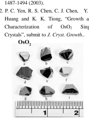
利用化學汽相傳輸法已成功地成長出
大尺寸且具有清晰刻面的 OsO2 單晶。利用
X-ray 粉晶繞射實驗,可定義出金紅石結構的
OsO2 晶體具有的所有可能繞射訊號位置及相
對強度。於 X-ray 光電子發射譜,亦指出 OsO2
單晶內所有對應 Os 及 O 原子之內層電子鍵結 能位置。OsO2單晶所量得之最低室溫電阻率約 為 15 -cm。另一方面,利用有機金屬化學汽 相沈積法,將系統壓力控制於 1 至 50 Torr 的範 圍內,實驗上亦成功地成長出 IrO2多晶薄膜及 具有(002)成長方向之 IrO2奈米柱。此類氧化物 之成長特性與可能機制,亦有深入的探討。透 過 X-ray 繞射與光電子發射譜,拉曼光譜,掃 描式與穿透式電子顯微鏡,電阻率以及場發射 的量測,IrO2薄膜與奈米柱之結構,化學組成,
結晶形貌以及電特性等資訊,皆能有效且深入 地加以探討。
五、參考文獻
1. D. B. Rogers, R. D. Shannon, A. W. Sleight and J. L. Gillson, Inorg. Chem. 8 (1969) 841.
1487-1494 (2003).
2. P. C. Yen, R. S. Chen, C. J. Chen, Y. S.
Huang and K. K. Tiong, “Growth and Characterization of OsO2 Single Crystals”, submit to J. Cryst. Growth..
Figure 1. Some representative crystals of OsO2
grown by chemical vapor transport method in our laboratory.
Figure 2. X-ray diffraction pattern of OsO2.
2. D. D. Sarma and C. N. R. Rao, J. Electron
Spectrosc. Relat. Phenom. 20 (1980) 25.
3. B. R. Chalamala, Y. Wei, R. H. Reuss, S.
Aggarwal, B. E. Gnade, R. Ramesh, J. M.
Bernhard, E. D. Sosa, D. E. Golden, Appl.
Phys. Lett. 74 (1999) 1394.
4. M. H. Huang, S. Mao, H. Feick, H. Yan, Y.
Wu, H. Kind, E. Weber, R. Russo, Y. Yang,
Science 292 (2001) 1897.
Figure 3. The temperature dependence of the resistivity in the range of 4.2 to 300 K for OsO2
singlecrystal.
Figure 5. FESEM images of the deposited Ir thin film (a, b) and the IrO2 thin film (c, d), showing both surface view and tilt-view of 45.
Figure 6. The resistivity as a function of temperature in the range between 16 and 300 K for the as-deposited Ir and IrO2 thin films deposited at Td =
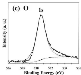
Figure 4. (a) The XPS spectrum of OsO2 single crystal. (b) Os 4f and 5p spectrum of OsO2 (solid line). The dot line shows the fitted 4f7/2 and 4f5/2 doublet components and 5p3/2
feature. (c) O1s spectrum of OsO2 (solid line) and the fitted curve (dot line).
Figure 8. FESEM images of the IrO2 nanorods grown on the Ti-coated-Si substrate: (a) top view; (b) 45 cross sectional view; (c) and (d) views of the nanorod with larger spiral-shaped tip.
400 C and Pd = 1 and 30 torr, respectively.
Figure 7. FESEM images of the IrO2 nanorods grown on the Si(100) substrate, taken from a tilting angle of 30 and with magnifications 20,000.
Figure 9. (a) The schematic diagram of a typical IrO2
nanorod. (b) TEM image focused on the tip of a nanorod and (c) its corresponding electron diffraction pattern taken along [010] zone axis.