國立臺灣大學電機資訊學院電信工程學研究所 碩士論文
Graduate Institute of Communication Engineering College of Electrical Engineering and Computer Science
National Taiwan University Master Thesis
應用於天文接收機之寬頻差動低雜訊放大器與應用於第五代 行動通訊之寬頻功率放大器設計
Design of Broadband Differential LNA for Radio Astronomy Receiver and Broadband PA for 5G Communication
范庭瑄
Ting-Hsuan Fan
指導教授:王暉 博士 Advisor: Huei Wang, Ph.D.
中華民國 110 年 2 月 February, 2021
誌謝
時光飛碩,兩年多的碩士生涯結束了,在電波這個領域,從懵懂無知的菜鳥 學習成長,如今得以完成這本論文、研究成果順利發表國際期刊,首先最感謝的 是指導教授—王暉博士,老師嚴謹的態度、優秀的數學能力、清晰的邏輯和論文 寫作上的精闢的提點,帶領著我走向老師一生輝煌、遙不可及的成就。同時,感 謝我的口試委員,黃天偉教授、林坤佑教授、蔡作敏教授、及天文所章朝盛博士,
感謝您們在口試上提供許多珍貴的意見,使本論文能更加完整。同時,特別感謝 章朝盛博士在每周的開會時與我討論研究上的方向、協助量測環境,碩士論文更 是逐字看過,給予我相當大的幫助,希望研究成果能順利發表在國際研討會。
在實驗室裡,感謝博士班學長陳俊年、王雲衫、林文傑、林宜賢、鍾杰穎,
不管在學業上或是生活上都給予許多經驗和無微不至的關心,使離鄉背井的我感 到溫暖。感謝助理陳淑貞小姐,在行政與會計事務的協助,使實驗室順利運作,
準時報帳領薪水,不會為了生計擔心,也要感謝碩士班學長陳穎、張洋、姜智穎、
唐子兼、黃煒程、李凱皇、呂伯澤、郭岱宥、許清閔、林彥廷、江坤展、徐浩翔、
陳育群、及學姊黎欣怡,在學時提點研究方向或畢業後找工作上,都持續關心、
帶領著我,使我屢屢突破難關。而實驗室的同學們,王子豪、陳毓閔,黃碧玲、
盧彥廷、張彥瑋、黃幕召、王婕葦,在這些日子裡一起互相學習幫助、一起度過 了無數壓力大趕下線的夜晚,課外舉辦相當多的活動使實驗室的生活不再陳悶,
給予我歡笑和動力。碩士班學弟妹中,謝謝梓洋,牧恆、煒智、楷懏、荷青、凱 傑、有東、傳立、育成、健平、家頤、羚毓、瑋軒、愛晨、俊嘉,即使相處的時 間不長,能帶給你們的東西不多,希望你們能繼續加油,讓實驗室再創高峰。
感謝我的朋友們,勸說我挑戰考取第一學府台大,並在我迷惘低潮時提供了 安慰與陪伴,感謝我的家人,總是支持我的選擇,還有好多好多要感謝的人,無 法一一提名,但每個人的關心、鼓勵,我都看在眼裡,更放在心中,謝謝你們。
最後感謝自己在每個挫折失眠、快要放棄的夜晚,持續堅持下去,在二十五 歲的今天許下願望,願往後未來在工作上或任何事都能努力不懈、勇往直前。
庭瑄 2021/02/01
中文摘要
低雜訊放大器在接收機系統中扮演重要角色。在射頻天文應用中,需要高靈 敏度的接收器。對於平方公里陣列,射頻望遠鏡的工作頻率範圍很寬。平方千米 陣列計畫中頻覆蓋 0.35 到 25 GHz 的頻率範圍,需要寬帶高增益低雜訊放大器。
這個頻帶被分成幾個子頻帶,其中一個子頻帶覆蓋 4.6 到 8.5 GHz 的頻率範圍。
此外,隨著第五代行動通訊的發展,毫米波的研究與應用已經成為現在的趨勢。
然而,對於頻寬及更高的傳輸速率需求與日俱增,其中,28 及 39 GHz 為第五代
行動通訊主要潛在發展頻段。
本篇論文主要分成兩個部分: 第一部分為接收器前端電路之低雜訊放大器相
關研究。藉由準確地選擇電路架構,在晶片上使用主動式寬頻巴倫來做系統整合,
此低雜訊放大器在 4.6 到 8.5 GHz 系統規格之頻帶內提供足夠增益(28 ± 1 dB)及 雜訊指數(1 ± 0.2 dB)。這個低雜訊放大器實現了差動輸入-單端輸出的架構。因此 它適用於下一代前端射頻天文接收器系統。
第二部分介紹了採用65nm CMOS 製造的 Ka 頻段寬頻功率放大器,其中設計
頻段是未來的5G 可行通信頻段(24 至 43GHz)。單級功率放大器提供26 至 41 GHz
的3-dB 頻寬和 24 至 41 GHz 的 52.3% 1-dB 飽和功率比例頻寬的大訊號性能,25
到37 GHz 的 38.2% 1-dB 增益壓縮點的比例頻寬和從 26 GHz 到 38 GHz 功率附加
效率皆超過20%。該功率放大器利用寬頻匹配技術來提供更好的頻寬表現。
關鍵字:平方公里陣列、高速電子遷移率電晶體、低雜訊放大器、第五代行動通 訊、互補式金氧半導體、功率放大器。
ABSTRACT
Array (SKA), the radio telescope has a wide operating frequency range. The SKA-mid array covering the frequency range of 0.35 to 25 GHz and requires a broadband high gain LNA. This band is divided into several sub-bands, where one of SKA band covers the frequency range of 4.6 to 8.5 GHz. Besides, with the development of the fifth-generation mobile communication (5G), the demand for bandwidth and higher transmission rates is increasing day by day. Among them, 28 and 38 GHz are the main potential development bands for the fifth-generation mobile communication.
This dissertation is divided into two parts. The first part is the research of low noise amplifier. By accurately selecting the circuit architecture, the fully on-chip broadband active balun is used for advanced system integration. This low noise amplifier provides peak gain (28 ± 1 dB) and noise figure (1 ± 0.2 dB) in the 4.6 to 8.5 GHz. This low noise amplifier achieves the differential input to single-ended output architecture. Hence, it is suitable for next-generation radio astronomical receiver system.
The second part presents a wideband power amplifier, where the design band is the future 5G feasible communication band (24 to 43GHz). The one-stage power amplifier provides 3-dB bandwidth from 26 to 41 GHz and wideband large-signal performance of 52.3% 1-dB Psat fractional bandwidth from 24 to 41 GHz, 38.2% OP1dB fractional bandwidth from 25 to 37 GHz, and a PAE above 20% from 26 to 38 GHz. This power amplifier utilizes a broadband matching technique to provide better bandwidth performance.
Keywords – Square Kilometre Array (SKA), pHEMT, Low Noise Amplifier, Fifth-Generation Communication, CMOS, Power Amplifier.
CONTENTS
口試委員會審定書 ... #
誌謝 ... ii
中文摘要 ...iv
ABSTRACT ...vi
CONTENTS ... viii
LIST OF FIGURES ...xi
LIST OF TABLES ... xvii
Chapter 1 Introduction ... 1
1.1 Background and Motivation ... 1
1.2 Literature Survey ... 3
1.2.1 LNAs and baluns around C-band to Ku-band ... 3
1.2.2 Ka-band PAs in CMOS Process ... 5
1.3 Contributions ... 7
1.3.1 Broadband High Gain DLNA ... 7
1.3.2 Broadband High Output Power PA ... 8
1.4 Thesis Organization ... 9
Chapter 2 A Broadband DLNA in 0.15-μm GaAs pHEMT Process for Radio Astronomical Receiver ... 10
2.1 Introduction ... 10
2.1.1 Square Kilometre Array Project ... 10
2.1.2 Noise Figure of the Entire System ... 13
2.1.3 Effects of CMRR on Noise Figure. ... 14
2.2 Circuit Design ... 18
2.2.1 Circuit Architecture ... 18
2.2.2 Device Size and Bias Point Selection ... 20
2.2.3 Inductive Source Degeneration ... 25
2.2.4 R-L-C Feedback Technique ... 28
2.2.5 The Proposed Broadband Active Balun ... 35
2.2.6 Overall Circuit Schematic and Simulation ... 46
2.3 Experimental Results and Discussions ... 53
2.3.1 DC Operating Point ... 53
2.3.2 3-port and 2-port S-parameter Measurement ... 55
2.3.3 Noise Figure Measurement ... 59
2.3.4 Large-Signal Measurement ... 60
2.4 Summary ... 60
Chapter 3 A Broadband Transformer-Based Power Amplifier in 65-nm CMOS Process for 5G Communication ... 62
3.1 Introduction ... 62
3.1.1 Distributed Amplifiers ... 63
3.1.2 Balance Amplifiers ... 64
3.1.3 Wideband Matching Networks ... 65
3.1.4 Summary of Wideband Matching Topologies ... 65
3.2 Circuit Design ... 66
3.2.1 Block Diagram and power budget ... 66
3.2.2 Device Size and Bias Selection ... 67
3.2.3 Neutralization Technique ... 69
3.2.4 Load-pull Simulation for Wideband Operation ... 71
3.2.6 Overall Wideband High Output Power PA... 81
3.3 Experimental Results and Discussions ... 86
3.3.1 DC Operating Point ... 86
3.3.2 S-parameters Measurements ... 87
3.3.3 Large-signal Measurements ... 88
3.3.4 Digital Modulation Measurement ... 90
3.4 Summary ... 95
Chapter 4 Conclusion ... 98
REFERENCE ... 99
LIST OF FIGURES
Fig. 2.1 The composition of the SKA1-mid telescope [1]. ... 11
Fig. 2.2 The dipole antenna with built-in passive balun and single-ended LNA. ... 16
Fig. 2.3 The simulated CMRR versus the phase imbalance of ideal LNA. ... 17
Fig. 2.4 The simulated CMRR versus the gain imbalance of ideal LNA. ... 17
Fig. 2.5 The simulated noise figure versus CMRR of ideal DLNA. ... 17
Fig. 2.6 Overall circuit architecture of the differential LNA. ... 19
Fig. 2.7 Maximum gain and minimum noise figure of transistor with total gate width of 200 μm under 1-V drain supply voltage. ... 21
Fig. 2.8 Maximum gain and minimum noise figure of transistor with different gate width under 1-V drain supply voltage. ... 21
Fig. 2.9 DC-IV curves of an 8-finger transistor with total gate width of 200 μm. ... 23
Fig. 2.10 Transconductance and drain current versus gate bias voltage with 1-V drain supply voltage. ... 23
Fig. 2.11 Maximum gain and minimum noise figure versus drain bias voltage under -1-V gate bias voltage. ... 24
Fig. 2.12 Maximum gain and minimum noise figure versus gate bias voltage under 1-V drain supply voltage. ... 24
Fig. 2.13 The circuit topology of the transistor with the source degeneration technique and its equivalent small-signal model. ... 26
Fig. 2.14 Sopt and S11* of the transistor of 8-finger with total gate width of 200 μm with different inductance of source degeneration from 0 to 500 pH. ... 26 Fig. 2.15 The simulated maximum gain and NFmin of the transistor of 4-fingers with total gate with of 200 μm with different inductance of source degeneration.27
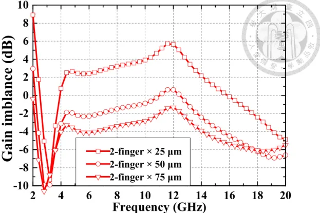
Fig. 2.16 The simulated stability factor of the transistor of 8-fingers with total gate with of 200 μm with different inductance of source degeneration. ... 27 Fig. 2.17 The circuit schematic and equivalent small-signal model of the transistor with the R-L-C feedback technique. ... 28 Fig. 2.18 The circuit schematic and equivalent small-signal model with Lf. ... 29 Fig. 2.19 The maximum gain and stability factor of the transistor of 4 fingers 25-μm gate width versus feedback inductance Lf at 6 GHz. ... 30 Fig. 2.20 The maximum gain of the transistor of 4 fingers and 25-μm gate width at different Lf value. ... 30 Fig. 2.21 The circuit schematic and equivalent small-signal model with Lf and CF. ... 31 Fig. 2.22 The maximum gain of the transistor of 4-fingers 200-μm total gate width with 3.5-nH Lf and different Cf. ... 32 Fig. 2.23 The stability factor of the transistor of 4-fingers 200-μm total gate width with 3.5-nH Lf and different Cf. ... 32 Fig. 2.24 The maximum gain of the transistor of 4 fingers 200-μm total gate width with feedback components which contains 3.5-nH Lf, 1-pF Cf and different Rf. . 33 Fig. 2.25 The stability factor of the transistor of 4 fingers 200-μm total gate width with feedback components which contains 3.5-nH Lf, 1-pF Cf and different Rf. . 34 Fig. 2.26 The pre-simulation of the concept of gain slope with each stage. ... 34 Fig. 2.27 The circuit schematic of the broadband matrix balun. ... 36 Fig. 2.28 Definition of the chain matrices used for calculating the S-parameters of the matrix balun [40]. ... 36 Fig. 2.29 The simulated gain imbalance of proposed matrix balun at different device
size of M2. ... 41 Fig. 2.30 The simulated phase imbalance of proposed matrix balun at different device
size of M2. ... 41
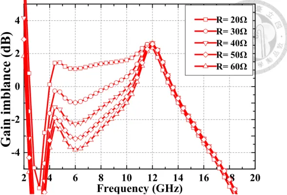
Fig. 2.31 The simulated gain imbalance of proposed matrix balun at different termination resistors R1. ... 42
Fig. 2.32 The simulated phase imbalance of proposed matrix balun at different termination resistors R1. ... 42
Fig. 2.33 The simulated gain imbalance of proposed matrix balun at different length of transmission line between M1 transistors. ... 43
Fig. 2.34 The simulated gain imbalance of proposed matrix balun at different length of transmission line between M1 transistors. ... 43
Fig. 2.35 The simulated S-parameters of the proposed broadband matrix balun. ... 44
Fig. 2.36 The simulated isolation of the proposed broadband matrix balun. ... 44
Fig. 2.37 The simulated gain and phase imbalance of matrix balun and passive L-C balun. ... 45
Fig. 2.38 Circuit schematic of the proposed broadband DLNA. ... 47
Fig. 2.39 The simulated mix-mode S-parameters of proposed DLNA with two different process. ... 47
Fig. 2.40 The simulated noise figure of proposed DLNA with two different process. ... 48
Fig. 2.41 3-port S-parameter simulation result of the DLNA. ... 48
Fig. 2.42 2-port S-parameter simulation result of the DLNA. ... 49
Fig. 2.43 Simulated noise figure and phase difference of the proposed DLNA. ... 49
Fig. 2.44 Simulated common-mode gain and CMRR of the proposed DLNA. ... 50
Fig. 2.45 The simulated stability factor (K) of the proposed DLNA. ... 51
Fig. 2.46 The post-layout time-domain simulation result of the DLNA. ... 52
Fig. 2.47 Chip layout of the proposed differential LNA with chip size 2 × 3 mm2. ... 52
Fig. 2.49 Measured and simulated 3-port S-parameters of the proposed DLNA. ... 56
Fig. 2.50 Measured and simulated 2-port differential mixed-mode S-parameters of the proposed DLNA. ... 56
Fig. 2.51 Measured phase imbalance of the proposed DLNA at different control voltage of matrix balun. ... 57
Fig. 2.52 Measured gain imbalance of the proposed DLNA at different control voltage of matrix balun. ... 57
Fig. 2.53 Measured common-mode gain and differential-mode gain of the proposed DLNA at different control voltage of matrix balun. ... 58
Fig. 2.54 Measured CMRR of the proposed DLNA at different control voltage of matrix balun. ... 58
Fig. 2.55 Measured and simulated noise figure of the proposed DLNA. ... 59
Fig. 2.56 The measured 1-dB compression point from 2 to 14 GHz of the proposed DLNA. ... 60
Fig. 3.1 Circuit architecture of conventional distributed amplifier. ... 63
Fig. 3.2 The block diagram of balanced amplifier. ... 64
Fig. 3.3 The block diagram and initial power budget of the proposed PA. ... 66
Fig. 3.4 ID and gm versus different VGS with the cascode cell... 67
Fig. 3.5 The 3D version of inter-digital compact layout of power cell with neutralization capacitors. ... 70
Fig. 3.6 The simulated stability factor and maximum gain with different neutralization capacitance values versus different frequency. ... 70
Fig. 3.7 Load-pull simulations of the power stage cells at 28 GHz. ... 72
Fig. 3.8 Load-pull simulations of the power stage cells at 38 GHz. ... 72
Fig. 3.9 Simulated optimal impedance on smith chart from 24 to 43 GHz. ... 72
Fig. 3.10 The schematic of transformer-based matching network ... 74
Fig. 3.11 Simulated the transformer impedance with different magnetic coupling coefficient k. ... 75
Fig. 3.12 Simulated insertion loss versus magnetic coupling coefficient at different frequency. ... 75
Fig. 3.13 The EM layout of low-impedance transmission line. ... 77
Fig. 3.14 The simulated impedance of output transformers at different load impedance ZL. ... 77
Fig. 3.15 The setup for checking the return loss of the matching network. ... 78
Fig. 3.16 The simulated impedance versus frequency. ... 78
Fig. 3.17 Return loss of the matching network when Zref equals to Zopt*/Zin. ... 78
Fig. 3.18 The layout of (a) no shield (b) floating shield (c) patterned ground shield. .... 79
Fig. 3.19 Simulated maximum gain of transformer with different shield topology. ... 79
Fig. 3.20 The simulated Zopt and small-signal conjugate matching impedance on Smith chart from 24 to 43 GHz at (a) output and (b) input matching network. ... 80
Fig. 3.21 Complete circuit schematic of the proposed power amplifier. ... 82
Fig. 3.22 Simulated S-parameters of the proposed wideband PA... 82
Fig. 3.23 Simulated large-signal performances at 28 GHz of the proposed PA. ... 83
Fig. 3.24 Simulated large-signal performances at 38 GHz of the proposed PA. ... 83
Fig. 3.25 Simulated large-signal performances of the proposed PA at 24 to 42 GHz. .... 84
Fig. 3.26 The simulated stability factor of the proposed PA. ... 84
Fig. 3.27 The post-layout time-domain simulation result of the proposed PA. ... 85
Fig. 3.28 Chip layout with dummy cells of the proposed PA. ... 85
Fig. 3.29 Chip micrograph with the size of 0.56 × 0.62 mm2 excluding all pads. ... 87
Fig. 3.31 Measured and simulated large-signal performances at 28 GHz. ... 88 Fig. 3.32 Measured and simulated large-signal performances at 38 GHz. ... 89 Fig. 3.33 Measured and simulated power performance vs. frequency of the proposed PA.
... 89 Fig. 3.34 The measured (a) constellation and (b) output spectrum of the proposed PA at the carrier frequencies of 28 GHz with 200 MHz channel bandwidth. ... 91 Fig. 3.35 The measured (a) constellation and (b) output spectrum of the proposed PA at the carrier frequencies of 38 GHz with 200 MHz channel bandwidth. ... 91 Fig. 3.36 The measured EVM versus average output power of 64-QAM signals with
0.6/1.2/2.4 Gbps data rates at 28GHz. ... 91 Fig. 3.37 The measured EVM versus average output power of 64-QAM signals with
0.6/1.2/2.4 Gbps data rates at 38GHz. ... 92 Fig. 3.38 The measured average output power under EVM -25 dBc versus RF frequency of 64-QAM signals with 0.6/1.2/2.4 Gbps data rates. ... 92 Fig. 3.39 The measured (a) constellation and (b) output spectrum at 28 GHz. ... 93 Fig. 3.40 The measured (a) constellation and (b) output spectrum at 38 GHz. ... 93 Fig. 3.41 The measured EVM of 64-QAM OFDM signals with 0.1/0.2/0.4/0.8 GHz
channel bandwidth at 28 GHz. ... 94 Fig. 3.42 The measured EVM of 64-QAM OFDM signals with 0.1/0.2/0.4/0.8 GHz
channel bandwidth at 38 GHz. ... 94 Fig. 3.43 The measured average output power under EVM -25 dBc versus RF frequency of 64-QAM OFDM signals with 0.1/0.2/0.4 GHz channel bandwidth. ... 95
LIST OF TABLES
Table 1.1 Summary of previously published LNAs and baluns. ... 4
Table 1.2 Summary of previously published Ka-band CMOS PAs. ... 6
Table 2.1 The three configurations in the SKA1 [1] ... 12
Table 2.2 The seven sub-frequency bands in SKA1-mid [1] ... 12
Table 2.3 Design goals of the proposed differential LNA. ... 19
Table 2.4 The bias conditions of the proposed DLNA. ... 54
Table 2.5 Summary of this work and published single-ended LNAs, DLNAs and Baluns61 Table 3.1 Load-pull simulation results of different conditions of the same device size. 68 Table 3.2 Voltage adjusted situation of the measurement. ... 86
Table 3.3 Comparison of this work and reported Ka-band CMOS PAs. ... 96
Table 3.4 Modulation comparison of this work and reported Ka-band CMOS PAs. ... 97
Chapter 1 Introduction
1.1 Background and Motivation
The international community has been constructed powerful observatories for inspecting unknown areas of the universe in the past few decades. Scientists are unable to explain many of the phenomena in the universe due to the limitations of optical telescopes. Therefore, radio telescopes which can receive radio to gamma-rays is an important tool to probe the universe in depth. The radio telescope with unprecedented high sensitivity, composed by a combination of thousands of radio receivers, allows astronomers to look into the formation and evolution of stars. The completion of the SKA1-mid will extremely enhance the performance of existing telescopes and become the largest telescope in similar frequency [1].
The Square Kilometre Array (SKA) project is a next-generation radio telescope that contains thousands of antennas over a square kilometer of the collecting area. The output signal-to-noise ratio (SNR) is a crucial parameter for radio astronomy receiver system.
The noise figure substantially impacts the overall SNR. Among the components of the receiver, the front-end component called low noise amplifier (LNA) dominates the noise figure of the entire receiver system. In the SKA project, the LNA in the system is used to supply low noise figure and high gain to improve the entire system SNR [2]. A LNA with differential input to single-ended output can reduce the noise figure. Formerly, it is difficult to achieve fully integrated differential LNA at low-frequency ranges because of the large on-chip passive components. Therefore, LNA with differential input and low noise figure is designed for reaching the requirement of radio astronomical receiver.
The fifth-generation mobile network (5G) is the main development direction of modern communications. The 5G development targets to increase data transmission rate and combine IoT applications. Another feature of 5G technology is the reduction of signal delay, which can develop high-precision applications. The frequency adopted around the world is gradually becoming clearer and can be roughly divided into two types [3]. The first is a band defined by 3GPP, ranging from 450 MHz to 6000 MHz, commonly referred to as the sub-6 GHz band. According to 5G NR standard, the second frequency bands such as n257, n258 and n260 from 24 to 43 GHz are allocated separately to various regions. This raises the need for wideband or multiband 5G transceivers to support international roaming [4].
Millimeter-wave technology can be used to meet the data transmission rate requirements, but must overcome the millimeter wave defects, including large air loss, and weak diffraction ability, which is easily blocked by obstacles. There have been several phased array designs to be realistically implemented for 5G applications which allow for a larger number of elements [5], [6], [7]. In a form-factor of handheld device, only a small number of elements can be physically integrated, thus dramatically increasing the requirement on the device saturated output power (Psat) to achieve a certain effective isotropic radiated power (EIRP) [8]. The required peak output power is estimated in the range of 18 to 24 dBm with an estimated required efficiency greater than 20%. Moreover, most of reported power amplifiers focused on pursuing high output power and high peak efficiency to present superior performances and overcame the disadvantage of poor air loss at millimeter-wave frequency. Therefore, power amplifiers with high power density, high efficiency, and wider bandwidth are desired for high speed 5G application in order to compete with the published state-of-the-arts PA and reach the requirements of the 5G application.
1.2 Literature Survey
The literature surveys include C-to-Ku band LNAs, baluns in GaAs process and Ka-band PAs in CMOS Process.
1.2.1 LNAs and baluns around C-band to Ku-band
The previously LNAs and baluns published around C-band to Ku-band are listed in Table 1.1. Comparing to differential-input to single-ended output low noise amplifier (DLNA) fabricated in CMOS process [10] [11], MMICs fabricated in III-V semiconductors are commonly used for radio astronomy receiver due to their superior performance to meet the requirement on low noise and high gain amplifiers. The fully-integrated DLNA is targeted on extremely wide bandwidth due to high sensitivity detection of the weak signals from the universe in the radio astronomy receiver system. Design of the wideband amplifiers, the negative feedback technique is commonly used for extending the bandwidth.
The inductive source degeneration is one of the negative feedback techniques for the common-source amplifier design [9]. Moreover, the resistive shunt feedback technique such as the R-L-C feedback technique is also utilized for wideband design. There are only two published DLNA fabricated in GaAs process at low-frequency range [12], [13]. A passive lumped LC balun which constructed by directly combining a 90° high-pass phase shifter with a 90° low-pass phase shifter is adopted. But, the disadvantages of on-chip passive baluns are high loss, enormous imbalances and limited bandwidth [14], [15]. Active baluns using matrix amplifiers topology demonstrate broad bandwidth with small gain variation [16]. On the other hand, it required large power consumption. However, in the design of DLNA, differential-mode gain and common-mode rejection ratio (CMRR) are important parameter to decide which is good or not and shows the competitiveness. Both of differential-mode gain and CMRR degrade due to the phase and gain imbalance of on-chip
balun and the phase error of the input differential signal. Therefore, to satisfy the need of radio receiver system, a high gain broadband fully-integrated DLNA with low imbalance balun is desired.
Table 1.1 Summary of previously published LNAs and baluns.
Ref. Process Topology 3-dB freq.
(GHz)
BW (%) Gain (dB) Pdc
(mW)
Noise Figure
(dB)
Amp.
Imbalance (dB)
Phase Imbalance
(°)
Area (mm2) RFIT [9]
2015
0.15-μm GaAs
pHEMT SE-LNA 3.2-14.7 127 31.7 45 1.3 - - 3.75 [10]
RFIC 2009
0.13-μm
CMOS DLNA 22.9-26.
4# 14.2 14.7 20.2 4.3 0.6 10* 0.82 [11]
TCASI 2018
0.18-μm SiGe
BiCMOS DLNA 17.5-25# 35.2 19.2 73.8 4 1 10.4 0.69 [12]
RFIT 2018
0.15-μm GaAs
pHEMT DLNA 1.5-3.7# 85 31.8 25 0.73 3.5* 48* 5 [13]
2019 IMS
0.15-μm GaAs
pHEMT DLNA 4.3-16.3# 116 35.4 90 1.05 0.5* 30* 5 [14]
2015 IMS
0.15-μm GaAs
pHEMT Balun 4.7-6.1 48 -2 0 - 0.63 3.7 1
[15]
EUMC 2018
0.1-μm GaAs
pHEMT Balun 9-20 75.8 -1.2 0 - 0.2 0.7 0.24
[16]
2011 IMS
0.15-μm GaAs
mHEMT Balun 4-40 163 3.5 53 - 2 20 1.08
*estimated from the date shown in paper or dissertation, #3-dB bandwidth of differential-mode gain
1.2.2 Ka-band PAs in CMOS Process
The previously PAs published Ka-band are listed in Table 1.2. The literatures of Ka-band power amplifier design reported in [22] and [25] show that the saturated output power (Psat) can be achieved up to 26 dBm in CMOS processes but narrow bandwidth. The stacked-PA topology overcame the low break-down voltage of the device and increased the optimum load impedance [20], [23]. However, the parasitic capacitance from intermediate node becomes significant. Thus, the phase of voltage swing at the drain of each stacked-transistor could not align, causes to degrading the power performance and the drain-source voltage swing possibly exceeds the breakdown voltage. The transformer-based power combining can be categorized into voltage-type and current-type. Some PAs designed with voltage-type combiner such as the distributed active transformer (DAT) [17]. However, different input impedances at each port of the DAT causes the serious imbalance problem which reduces the power combing efficiency. PAs used current-type combiner [17] [21]
have low voltage and phase imbalances, but the layout area and insertion loss of current-type combiners are often larger than that of voltage-type combiners. The combiner used in [24] is based on synthesis methodology which performs the necessary impedance modulation, matching to desired output load impedance and lower loss compared to the combiner of conventional Doherty PAs. However, the load modulation of Doherty PAs is complex and a wider bandwidth is hard to achieve in the Doherty PAs. The technique of increasing transistor-size is the intuitive way to improve Psat, but the drawback is that the parasitic capacitance will also be increased proportionally which causes the optimal impedance lower. The matching network requires a high impedance transformation ratio to match the impedance ZL, and this often results in high passive loss. Therefore, to achieve a wideband high output power PA, the main challenge is to design the low loss broadband matching networks.
Table 1.2 Summary of previously published Ka-band CMOS PAs.
Ref. Process
3-dB (GHzBW.
)
Gain (dB) Psat
(dB) OP1dB
(dBm) PAEMAX
(%)
1-dB Psat
BW (%) 1-dB
P1dB
BW (%)
P.D.**
(mW/mm2) Area (mm2) [17]
ISSCC 2020
45-nm
CMOS SOI 26-43 20.5 20.4 19.1 45 51 51 77.8 1.35
[18]
JSSC 2018
28-nm
CMOS 29-57 20.8 16.6 13.4 24.2 56.
6 32.
3 95.2 0.48 [19]
TMTT 2015
65-nm
CMOS 33-46 19.4 26.8 - 10 32.9* - 115.1 4.16 [20]
JSSC 2016
45-nm
CMOS SOI 24-35 13 24.8 21 26 31.6* - 1006.6 0.3
[21]
2017 IMS
90-nm
CMOS 14-24 14.1 24.4 21.7 28 26.1* 18.2* 523.6 0.526 [22]
TMTT 2019
90-nm
CMOS 21-31 16.3 26 23.2 34.1 30.8* 35.3* 992.8 0.401 [23]
2019 IMS
65-nm
CMOS 33-42 17.5 24.8 21.2 24.3 21.9* 23.4* 816.2 0.37*
[24]
PAWR 2019
45-nm
CMOS SOI 24-29 10 25 24.2 31 18.8* - 683.8 0.63
[25]
RFIC 2019
28-nm
CMOS 37-39 38 26 21.5 26.6 14 - 419.1 0.95 [26]
2020 IMS
28-nm
CMOS 21-41.6 20.4 15.5 12.7 35.3 50.4 18.2 98.5 0.36*
*estimated from the date shown in paper
1.3 Contributions
This dissertation presents a broadband high gain DLNA for SKA application, and a broadband high output power PA for 5G application. The contribution of these works will be introduced as following.
1.3.1 Broadband High Gain DLNA
In the first part, a DLNA using 0.15-μm GaAs pHEMT process designed for the SKA band from 4.6 to 8.5 GHz will be presented. In previously published works, it is a challenge to achieve low noise and compact layout at such wide bandwidth designed with differential input to single-ended output structure. If the isolation, gain imbalance and phase imbalance between two input ports are poor, accompanying the common-mode rejection ratio (CMRR) degrades which will affect the overall circuit performance. In this work, in order to achieve better performance, the inductive source degeneration is adopted in the first and second stage for the lower noise figure, and the R-L-C feedback technique is used in the third stage for wideband design. For the differential input to single-ended output design, a broadband active balun is firstly proposed to adjust gain and phase imbalance for better CMRR and resolve the disadvantages of on-chip passive balun such as high loss, enormous imbalance and limited bandwidth.
The proposed DLNA shows 3-dB small-signal gain bandwidth from 3.3 to 11.3 GHz and 28.3-dB peak gain, average noise figure of 1.4 dB with dc power consumption of 85 mW. Compared to publish C-band to Ku-band HEMT-based LNAs [8] - [15], this DLNA demonstrates the best CMRR in the near frequency range.
1.3.2 Broadband High Output Power PA
A wideband high output power PA fabricated in 65-nm CMOS is demonstrated. In this work, the studies are focused on the wideband matching technique through the transformer-based matching network. In order to alleviate a very high impedance transformation ratio caused by a larger transistor-size, the slotted low impedance transmission line is adopted which has a feature to lower the magnitude of load impedance. Hence, it will be easier for the output combiner to transform the load impedance to the optimum impedance required for each power stage cells. Besides, most reported wideband PAs at millimeter-wave frequencies only support wideband small-signal gain, not actual wideband operation at large-signal region [46], [47], [48]. In this work, by changing the second resonant frequency of the transformers, the lower variation of load impedance of transformer versus frequency can be reached. Therefore, the optimum impedance can be obtained with the broadband matching network without extra lumped elements to avoid additional passive loss. Due to the high output power, this work possesses a large voltage swing which then facilitates the electric field of transformers. The floating shields diminish the eddy current by preventing the electric field leaking to the substrate and also limit parasitic magnetic coupling effects between two transformers.
These design features facilitate the proposed wideband power amplifier to achieve 3-dB bandwidth from 26 to 41 GHz and wideband large-signal performance of 52.3%
1-dB Psat fractional bandwidth from 24 to 41 GHz, 38.2% OP1dB BW from 25 to 37 GHz, and PAE above 20% from 26 to 38 GHz. Among the published Ka-band PAs [16] - [24], this work offers a superior output power bandwidth performance. This work has been published in 2020 MWCL [57].
1.4 Thesis Organization
The organization of this thesis is shown as follows.
In chapter 2, a broadband high-gain DLNA in 0.15-μm GaAs pHEMT process is designed and measured. The design procedures including device size selection, source degeneration technique, R-L-C feedback technique and broadband active balun are demonstrates. The simulated and measured results are shown. And a short conclusion is presented at the end of this chapter.
In chapter 3, a wideband high output power PA with a broadband matching network is demonstrated and measured. The design procedures including neutralization technique, broadband matching technique, patterned floating shield structure and overall simulation are described. The simulated and measured results are shown. And a short conclusion is presented at the end of this chapter.
Finally, a conclusion of this thesis is given in Chapter 4.
Chapter 2 A Broadband DLNA in 0.15-μm GaAs pHEMT Process for Radio Astronomical Receiver
In this chapter, a fully-integrated DLNA with differential input and single-ended output using broadband active balun is presented in this chapter. The proposed DLNA used inductive source degeneration to lower the noise figure and R-L-C feedback to implement wideband design. The fully on-chip broadband active balun is used for wider differential-to-single conversion bandwidth. This work utilizes the method of noise figure measurement for the 3-port differential-input-to-single-ended output amplifiers [12]. The 3-dB small-signal gain bandwidth covers from 3.3 to 11.3 GHz. The measurement results show 28.3-dB peak gain and average noise figure of 1.4 dB with dc power consumption of 85 mW.
Equation Chapter 2 Section 1
2.1 Introduction
2.1.1 Square Kilometre Array Project
The Square Kilometre Array (SKA) project is an on-going project to devise and implement a new radio telescope array receiver for many years. SKA project is not only a telescope, but a group of telescopes called arrays that can spread to long distances. The SKA project is going to construct a huge antenna array, including approximately 130,000 antennas between 500 stations in Australia and South Africa. Furthermore, there are other projects proceed in Mexico and Arizona State in the northern hemisphere to simulate enormous telescopes as large as Earth. The central control room composes the universe data received by each antenna into more manageable information. It will have higher sensitivity and instantaneous field of view than any current telescopes. These advantages
will ensure that SKA project has a great influence on solving nowadays major astrophysics and cosmology problems. The composition of the entire SKA antenna array is shown in Fig. 2.1. The location of the antennas is located in the core and in the three spiral arms which has different arm lengths and angles. The shaped spiral arms arrangement of this antenna enables high resolution imaging capabilities of the entire radio observatory. The development of SKA project is carried out through cooperation on a global scale. For radio astronomy receiving system, the dipole antennas are commonly used for their simplicity [27]. It is suitable for large array project requiring millions of antennas such as SKA project which can be mass-produced [1]. In addition, both polarizations of the incoming signal from the sky are received and processed to increase the detection sensitivity, also a useful tool to mitigate artificial radio frequency interference (RFI) and to derive magnetic field information toward the source.
Fig. 2.1 The composition of the SKA1-mid telescope [1].
In the beginning, the first phase of SKA project divides the total bandwidth of the receiver into three parts, SKA1-low covers from 50 to 350 MHz, SKA1-mid covers from 350 to 13800 MHz, and SKA1-survey covers from 650 to 1670 MHz [1], [2]. The three configurations of the first phase the telescope (SKA1) is shown in Table 2.1.
Nowadays, the higher frequency range of SKA1-mid extended to 25 GHz. Table 2.2 shows the seven sub-frequency bands in SKA1-mid [1].
Table 2.1 The three configurations in the SKA1 [1]
SKA1-low SKA1-mid SKA1-survey
Frequency (MHz) 50-350 350-13800 650-1670
Location Australia South Africa Australia
Table 2.2 The seven sub-frequency bands in SKA1-mid [1]
SKA1-mid
Band Frequency range (GHz) Bandwidth (%)
Band-1 0.35-1.05 100
Band-2 0.95-1.76 59.8
Band-3 1.65-3.05 59.6
Band-4 2.8-5.18 59.6
Band-5a 4.6-8.5 55.3
Band-5b 8.3-15.4 59.9
Band-6 13.5-25 59.7
2.1.2 Noise Figure of the Entire System
Because the signal received from the universe is rather weak, the sensitivity (Si) of the radio astronomy receiver is important. The sensitivity of the receiver is highly correlated with the receiving capability of the signal power which can be expressed as following [28]:
Si 0 o
o
kT B S NF N
= × ×
(2.1) where k represents the Boltzmann constant, T0 represents the absolute temperature, B represents the bandwidth of the receiver system, NF represents the noise figure, and SNRmin represents the minimum signal-to-noise ratio required by the receiver output port to process the signal. The kT0B can be calculated as the input noise floor of the receiver.
The receiver has good noise floor and sensitivity performance at lower temperatures in the system. For the reason that radio astronomy receivers commonly operate in cryogenic temperature environment. According to (2.1), the lower the system noise figure, the better the sensitivity of the receiver. The noise figure of a total system can be defined as following [29]:
( )
3 1 2
1 1 2 1 1
1 1
1 ... n
total
A A A A A n
NF NF
NF NF NF
G G G G G −
− −
= + − + + + (2.2)
where NFi represents the noise figure of each stage, and GAi represents the gain of each stage. According to (2.2), the noise figure of the entire system will be dominated by the noise figure of the forward stages.
2.1.3 Effects of CMRR on Noise Figure
In general, dipole antennas and built-in passive baluns are usually designed together as shown in Fig. 2.2. However, if there is a passive component without gain in front of the LNA, the noise figure of entire system will be severely increased, thereby reducing the receiver sensitivity. To reduce the noise figure of entire system, it is always desired to place LNA infront of power combiner as close as possible to the antenna feed. Therefore, LNA with differential input and power combining after signal amplification is an effective choice for this type of front-end receiver. Furthermore, differential topology provides better common-mode interference noise rejection and higher dynamic range when compared with single-ended-to-single-ended LNA.
From [42], the time domain output voltage of the LNA in differential-mode (vdiff) with the phase and gain imbalance of balun can be expressed as
diff1( ) A0cos( )0t A0cos( 0t )
v t = ω + ω +θ (2.3)
0
diff2( ) A (1 A)cos 0t
v t = + ω (2.4)
where θ and A denotes as the phase and gain imbalance of balun. By phasor notation, (2.3) and (2.4) can be expressed as
0(1 j ) A eθ
= +
diff 1
V (2.5)
0(1 )
A A
= +
diff2
V (2.6)
(2.5) can be rewritten as
2 2 1 2
0 (1 cos ) sin tan ( sin tan ) 2 2cos 0
1 cos 2
A θ θ θ θ θ A ejθ
θ
= + + ∠ − = = + ×
diff 1 +
V (2.7)
Then, comparing to the ideal case (Vdiff = 2A0), the differential voltage gain degradation
( (imbalance)
(ideal) GDEG = diff
diff
V
V ) in dB due to the phase and gain imbalance can be expressed as
DEG1 20log( 2 2cos )
G = − +2 θ (2.8)
DEG2 20log[(1 )]
G = − +2A (2.9)
However, the common-mode rejection ratio (CMRR) of the DLNA is related to the differential-mode gain and common-mode gain. Ideally, the common-mode gain is eliminated after being combined by 180° balun. On the other hands, the common-mode gain increased due to higher phase or gain imbalance of the DLNA which leads to poor CMRR. The output voltage of the LNA in common-mode (Vcomm) can be expressed as
comm1( ) 0cos( ) 0cos( )
v t =A ωt −A ω θt+ (2.10)
0
comm2( ) A (1 A)cos 0t
v t = − ω (2.11)
By using the phasor notation, (2.12) and (2.13) can be expressed as
0(1 j ) A eθ
= −
comm1
V (2.12)
0(1 )
A A
= −
comm2
V (2.13)
(2.12) can be rewritten as
( )
2 2 1 2 2
0 (1 cos ) sin tan ( sin cot ) 2 2cos 0
1 cos 2
A θ θ θ θ θ A ej π θ
θ
− − +
= − + ∠ = − = − ×
comm1 −
V (2.14)
Following the same derivation procedure of differential mode gain degradation, it can be found that the common-mode voltage gain enhancement (GEN) in dB due to the phase and gain imbalance can be expressed as
EN1 20log( 2 2cos )
G = −2 θ (2.15)
EN2 20log((1 ))
G = −2A (2.16)
Based on (2.8), (2.9), (2.15) and (2.16), CMRR can be expressed as
1 DM- CM 20l 2 2cos
CMRR og
= 2 2
G G cosθ
θ
+
= − (2.17)
2 DM- CM 20log 1
CMR = ( )
R G G 1 A
A
= +
− (2.18)
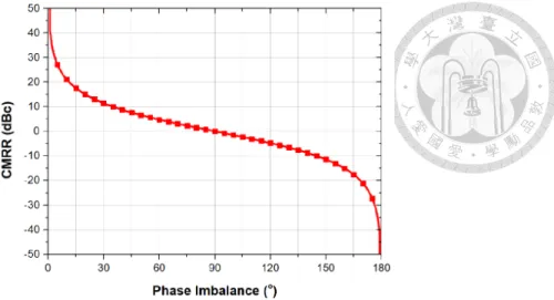
From (2.17) and (2.18), CMRR is affected by both phase imbalance and gain imbalance of DLNA as shown in the Figs. 2.3 and 2.4. It is well known that poor CMRR will reduce the noise performance of the entire system. As the phase and gain imbalance increased, the common-mode gain increased rapidly and the differential-mode gain also reduced in the meantime. In order to reduce the common-mode gain, the required phase and gain imbalance of DLNA must be below 10° and 0.5 dB. Fig. 2.5 shows the simulated noise figure of the DLNA versus CMRR. In conclusion, when the CMRR is greater than 20 dBc, the noise figure is not affected significantly.
Fig. 2.2 The dipole antenna with built-in passive balun and single-ended LNA.
Fig. 2.3 The simulated CMRR versus the phase imbalance of ideal LNA.
0 1 2 3 4 5 6 7 8 9 10
0 10 20 30 40 50
CMRR (dB)
Gain Imbalance (dB)
Fig. 2.4 The simulated CMRR versus the gain imbalance of ideal LNA.
-20 -10 0 10 20 30
0 2 4 6 8 10
Noise Figure (dB)
CMRR (dBc)
Fig. 2.5 The simulated noise figure versus CMRR of ideal DLNA.
2.2 Circuit Design
2.2.1 Circuit Architecture
The overall circuit architecture is shown in Fig. 2.6. The DLNA is composed of two LNAs and a broadband active balun. The LNA is designed for three stages to provide high gain. Theoretically, the design of first stage of the LNA is the most important part.
Because of the noise figure and gain considerations, the common-source structure using inductive source degeneration is adopted which is imposed to the first and second stage to minimize the noise figure. In the third stages, the R-L-C feedback technique is utilized to improve the flatness and width of the overall bandwidth.
There are many topologies to realize the structure of DLNA. Passive baluns are bi-directional converters between differential and single-ended signals. The rat-race coupler is possible to deploy the coupler as a 180° phase-shifted output divider or to combine two 180° phase-shifted signals with low insertion loss. The rat-race coupler provides good return loss at each port and good isolation between each port [30].
However, the bandwidth of rat-race couplers is relatively narrow, and therefore it is not suitable for broadband design. The Marchand balun is another structure that offers outstanding phase imbalance and gain imbalance. However, for operation in target frequency range from 4.6 to 8.5 GHz, the size required for the Marchand balun is large accompanying with huge insertion loss [31]. Hence, active balun is adopted in this work due to a wider bandwidth comparing to passive balun, even if active balun is only for unidirectional conversion. Since the gain provided by the active balun is not high enough to reduce overall noise figure. If the active balun is placed between the first stage and the second stage, it will affect the performance of the noise figure and isolation between two input ports. Therefore, the broadband active balun is place after the third
stage. This way to implement DLNA is suitable for circuits that require wider bandwidth. The design goals of the proposed DLNA are listed in Table 2.3.
RF
outG S G
G S G
RF
in G S3-stage LNA
Active balun
feedbackRLC Source
degeneration Source
degeneration
Fig. 2.6 Overall circuit architecture of the differential LNA.
Table 2.3 Design goals of the proposed differential LNA.
Process WIN 0.15-µm GaAs pHEMT (PP1555)
Frequency 4.6 to 8.5 GHz
Differential-mode Gain > 25 dB Differential-port Isolation > 20 dB
Noise Figure as low as possible
Gain imbalance 0.5 dB
Phase imbalance 10°
DC Power Consumption as low as possible
Gain flatness < 1 dB
OP1dB > 0 dBm
2.2.2 Device Size and Bias Point Selection
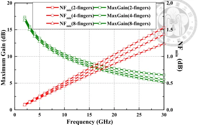
In the design of a low noise amplifier, the transistors size and bias condition should be decided as the first step for optimizing the performance of the LNA. In the HEMT process, the parasitic gate resistance (Rg) of transistors will be decreased when the number of fingers increase under a fixed total gate width. The Rg is inversely related to the minimum noise figure (NFmin). Therefore, it is normally to select multi-fingers transistors to achieve lower noise figure. The amount of gate fingers is compared within a selectable range of WIN GaAs pHEMT process manual. Fig. 2.7 shows the maximum gain and NFmin with the same total gate width of 200 μm under 1-V drain supply voltage.
Considering to the NFmin, the 8-fingers transistor is selected. With a fixed number of fingers, the Rg of the transistor also increases proportionally when increases the gate width of the transistors. Fig. 2.8 shows the maximum gain and NFmin with different gate width of the transistors under 1-V drain supply voltage. In the first and second stage, to get the best NFmin, the coplanar waveguide (CPW) type transistor size of 8-fingers and 25-μm gate width is chosen. The same device size selection procedure is used in the third stage. Because the tradeoff between gain and noise figure, the microstrip (MS) type transistor size of 4-fingers and 50-μm gate width is selected for the third stage.
0 5 10 15 20 25 30 0
5 10 15 20
NF
min(d B)
Maximum Gain (dB)
Frequency (GHz)
0.0 0.5 1.0 1.5 NFmin(2-fingers) MaxGain(2-fingers) 2.0
NFmin(4-fingers) MaxGain(4-fingers) NFmin(8-fingers) MaxGain(8-fingers)
Fig. 2.7 Maximum gain and minimum noise figure of transistor with total gate width of 200 μm under 1-V drain supply voltage.
0 5 10 15 20 25 30
0 5 10 15 20
NF
min(d B)
Maximum Gain (dB)
Frequency (GHz)
0 1 2 3
NFmin (25µm) Maximum Gain(25µm) 4
NFmin (75µm) Maximum Gain(75µm) NFmin (125µm) Maximum Gain(125µm)
Fig. 2.8 Maximum gain and minimum noise figure of transistor with different gate width under 1-V drain supply voltage.
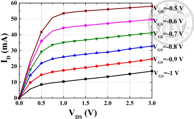
After selecting the transistors size, the DC bias needs to be decided which affects the noise figure and gain performance of the common-source transistor. The DC-IV curves of transistor with 8-fingers and 25-μm gate width is shown in Fig. 2.9.
For the cryogenic operation, the DC power consumption is required as low as possible to minimize heat dissipation. Fig. 2.10 shows the transconductance (gm) and drain current (ID) versus gate bias voltage (VGS). In the HEMT process, the best noise figure performance of the device usually operates from 50% to 70% ID at the peak gm
which means that the gate bias voltage (VGS) should select from -0.8 V to -0.9 V providing the least noise figure with sufficient gain.
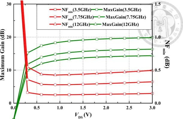
The maximum gain and the minimum noise figure (NFmin) under different bias condition are simulated. The simulation results are shown in Fig. 2.11 and Fig. 2.12.
When drain voltage (VDS) biases more than 1 V, the maximum gain is barely increased.
Therefore, the lower drain voltage can consume less dc consumption without reducing the small-signal gain. Fig. 2.11 shows the MSG and NFmin versus drain voltage of an 8-finger and 25-μm gate width common-source transistor under -1-V gate bias voltage. It demonstrates that the change of MSG and NFmin is not obvious when the drain supply voltage is higher than 1-V. Therefore, in order to reduce the power consumption without degrading the noise figure performance, the drain voltage is selected at 1-V. Fig. 2.12 shows MSG and NFmin versus gate bias of an 8-finger and 25-μm gate width common-source transistor under 1-V drain voltage. It demonstrates that the NFmin
reaches a minimum and the MSG reaches the maximum when VG is -0.8V. The candidate bias condition of measured S-parameters of transistors are -1.25, -1, -0.75 V. When the bias voltage is -1 V, the drain current is about 30% ID at the peak gm. When the bias voltage is -0.75 V, the drain current is about 100% ID at the peak gm. Thus, in order to reduce the power consumption, the gate bias voltage is selected at -1 V.
0.0 0.5 1.0 1.5 2.0 2.5 3.0 0
10 20 30 40 50
60
V
GS=-0.5 V
V
GS=-1 V V
GS=-0.9 V V
GS=-0.8 V V
GS=-0.7 V V
GS=-0.6 V
I
D(mA )
V
DS(V)
Fig. 2.9 DC-IV curves of an 8-finger transistor with total gate width of 200 μm.
-2.0 -1.5 -1.0 -0.5 0.0 0.5 1.0 1.5 0
30 60 90 120 150
I
Dg
mI
D(mA ), g
m(mS )
V
GS(V)
Fig. 2.10 Transconductance and drain current versus gate bias voltage with 1-V drain supply voltage.
0.0 0.5 1.0 1.5 2.0 2.5 3.0 0
10 20 30
NF
min(d B)
Maximum Gain (dB)
VDS (V)
0.0 0.5 1.0 NFmin(3.5GHz) MaxGain(3.5GHz) 1.5
NFmin(7.75GHz) MaxGain(7.75GHz) NFmin(12GHz) MaxGain(12GHz)
Fig. 2.11 Maximum gain and minimum noise figure versus drain bias voltage under -1-V gate bias voltage.
-1.5 -1.4 -1.3 -1.2 -1.1 -1.0 -0.9 -0.8 -0.7 -0.6 -0.5 0
10 20 30
NF
min(d B)
M ax im um G ain (d B)
V
GS(V)
0.0 0.5 1.0 NFmin(3.5GHz) MaxGain(3.5GHz) 1.5
NFmin(7.75GHz) MaxGain(7.75GHz) NFmin(12GHz) MaxGain(12GHz)
Fig. 2.12 Maximum gain and minimum noise figure versus gate bias voltage under 1-V drain supply voltage.
2.2.3 Inductive Source Degeneration
The inductive source degeneration is one of the negative feedback techniques for the low noise amplifier design. By connecting a degenerated inductor in series between the source terminal of the common-source transistor and the ground, the conjugate input impedance (S11*) can be shifted to the optimum source impedance for noise matching (Sopt). The minimum noise figure (NFmin) and stability factor will be improved simultaneously through adding an inductor at source terminal of transistor. The circuit topology of the transistor with the inductive source degeneration technique is shown in Fig. 2.13. Fig. 2.14 demonstrates S11* and Sopt with different source degeneration inductance. From Fig. 2.14, the S11* is shifted to Sopt, which means that the input return loss can be improved when noise matching is applied to the common-source transistor.
However, inductive source degeneration (Ls) degrades the gain. Therefore, Ls cannot be too large; otherwise, the gain will be severely decrease.
Maximum gain and NFmin of the transistor with the different source degeneration inductor are shown in Fig. 2.15. The transistor size is 8-fingers and 25-µm gate width.
As the ideal inductance increases, it can be observed that the maximum gain of the transistor will decrease and the NFmin also decreases slightly. The stability factor with different source degeneration inductance is shown in Fig. 2.16. When the inductance is greater than 400 pH, the stability factor of 9 GHz is almost greater than unity. The common-source transistors have better NFmin, a sharper negative gain slope, higher stability factor by selecting the larger inductance and the noise impedance is easier to matching. Hence, the tradeoff between maximum gain, NFmin and stability factor must be considered. After carefully simulating, the inductance of Ls is selected as 500 pH in the first stage and 250 pH in the second stage.
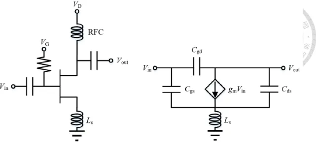
Fig. 2.13 The circuit topology of the transistor with the source degeneration technique and its equivalent small-signal model.
0.2 0.5 1.0 2.0 5.0 -0.2j
0.2j
-0.5j 0.5j
-1.0j 1.0j
-2.0j 2.0j
-5.0j
f H 5.0j L
s=500 pH
S
11* S
optL
s=0 pH
f L
Fig. 2.14 Sopt and S11* of the transistor of 8-finger with total gate width of 200 μm with different inductance of source degeneration from 0 to 500 pH.
Fig. 2.15 The simulated maximum gain and NFmin of the transistor of 4-fingers with total gate with of 200 μm with different inductance of source degeneration.
5 10 15 20
0.0 0.2 0.4 0.6 0.8 1.0
0pH 300pH 100pH 400pH 200pH 500pH
Stability Factor
Frequency (GHz)
Fig. 2.16 The simulated stability factor of the transistor of 8-fingers with total gate with of 200 μm with different inductance of source degeneration.
2.2.4 R-L-C Feedback Technique
The R-L-C negative feedback technique is adopted in this work for compensating the gain at high frequencies and producing a positive gain slope. The feedback resistor (Rf), feedback capacitor (Cf) and feedback inductor (Lf) are connected in series. Fig.
2.17 shows the circuit schematic and equivalent small-signal model of the transistor with the R-L-C feedback. The principle of this technique is that the feedback inductor (Lf) provides large inductance to resonate the gate-to-drain intrinsic capacitor (Cgd) of the transistor and increases the reverse isolation of the transistor. The poor reverse isolation degrades the performance of the maximum gain and destabilizes the transistor.
The reverse isolation directly affects the S12 of the transistor. Cgd can be resonated by selecting the Lf inductor in parallel with Cgd. Therefore, maximum gain and stability will be improved apparently. The feedback capacitor (Cf) is used to block DC current between the drain and the gate of transistors. Through R-L-C feedback, the gain is boosted at high frequencies and reduced at low frequencies which can improve the flatness of the overall bandwidth and make the bandwidth wider.
Fig. 2.17 The circuit schematic and equivalent small-signal model of the transistor with the R-L-C feedback technique.
In order to explain the main concept, the circuit is temporarily simplified, and the effects of Cf and Rf are ignored. Therefore, the circuit schematic and equivalent small-signal model of the transistor with only Lf and ideal DC block are shown in Fig.
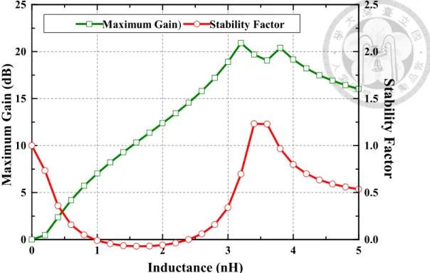
2.18. The ideal blocking capacitor is just used to separate DC level between the drain and the gate of transistors. Fig. 2.19 shows the maximum gain and stability factor of the transistor with different Lf at 6 GHz. When Lf is 3 nH, the peak maximum gain of transistor appears. According to the simulation, the maximum gain of the transistors with Lf is 8-dB higher than the transistors without Lf. The stability factor is about unity.
Fig. 2.20 shows the maximum gain of the transistor of 4 fingers and 50-μm gate width at different Lf value. At each resonant frequency, the maximum gain of each curve is larger than the original. By using a feedback inductor, the maximum gain of the transistor is effectively reduced in the lower frequency. The maximum gain at 4 GHz is reduced by approximately 10 dB with 3.5-nH Lf. Moreover, the resonant frequency becomes lower as the Lf increases. The Lf can be adjusted and optimized for the required maximum gain and gain slope. If Lf approach infinity and maximum gain curve will be the same as the original maximum gain curve, this is a special case.
Fig. 2.18 The circuit schematic and equivalent small-signal model with Lf.