I
行政院國家科學委員會補助專題研究計畫 □ 成 果 報 告
■ 期中進度報告
過渡性金屬氧化物及硫屬化合物之製備、特性研究 及其可能應用之探討(2/3)
Growth, Characterization and Applications of Transition Metal Dioxide and Dichalcogenide Compounds (2/3)
計 畫 類 別 : ■ 個 別 型 計 畫 □ 整 合 型 計 畫 計 畫 編 號 : NSC 92 - 2112 - M - 011 - 001 執行期間: 92 年 8 月 1 日 至 93 年 7 月 31 日
計 畫 主 持 人 : 黃 鶯 聲
計畫參與人員:嚴本嘉、陳瑞山
國立台灣科技大學電子工程所博士班研究生 劉彥堂
國立台灣科技大學電子工程所碩士班研究生 姚清偉、張弘民、蔡宗穎
國立台灣科技大學材料工程所碩士班研究生
成果報告類型(依經費核定清單規定繳交):■精簡報告 □完整報告
本成果報告包括以下應繳交之附件:
□赴國外出差或研習心得報告一份
□出席國際學術會議心得報告及發表之論文各一份
處理方式:除產學合作研究計畫、提升產業技術及人才培育研究計畫、列管計畫 及下列情形者外,得立即公開查詢
□涉及專利或其他智慧財產權,□一年□二年後可公開查詢
執行單位:國立台灣科技大學電子工程所
中 華 民 國 93 年 6 月 15 日
II
行政院國家科學委員會專題研究計畫期中精簡報告
過渡性金屬氧化物及硫屬化合物之製備、特性研究及其可能應用之探討
Growth, Characterization and Applications of Transition Metal Dioxide and Dichalcogenide Compounds
計劃編號:NSC92-2112-M-011-001 執行期限:92 年 8 月 1 日至 93 年 7 月 31 日 主持人:黃鶯聲 國立台灣科技大學電子工程系
計畫參與人員:嚴本嘉、陳瑞山、
劉彥堂、姚清偉、
張弘民、蔡宗穎
一、中文摘要
本計畫目的在從事過 渡 金 屬 硫 屬 化 合 物 單 晶 以 及 過 渡 金 屬 氧 化 物 薄 膜 與 奈 米 材 料 的 製 備 , 特 性 研 究 及 其 可 能 應 用 之 探 討 。 具 層 狀 結 構 的 金 屬 硫 合 物(ReS2, R eSe2, Mo S2, MoS e2, WS2, WSe2) 單 晶 與 傳 統 塊 狀 金 屬 氧 化 物 (Ru O2, IrO2, Os O2)單晶皆採 用化學汽 相傳輸方式成長。金 屬 氧 化 物 (RuO2, IrO2, OsO2) 薄 膜 與 奈 米 材 料 的 製 備 乃 使 用 應 用 性 較 高 的 有 機 金 屬 化 學 汽 相 沈 積 法 。 在 樣 品 特 性 量 測 方 面 , 各 種 調 制 反 射 光 譜 技 術 將 運 用 於 研 究 金 屬 硫 合 物 之 能 帶 結 構 與 載 子 躍 遷 情 形 。 利用 X 光繞射與拉曼散射實驗,可檢 測 單 晶 或 薄 膜 樣 品 之 結 構 特 性 與 結 晶 品 質 。 掃 瞄 式 與 穿 透 式 電 子 顯 微 鏡 影 像 用 以 觀 察 薄 膜 與 奈 米 材 料 表 面 形 貌 與微結構特性。
關鍵詞:過 渡 金 屬 硫 屬 化 合 物 、過 渡 金 屬 氧 化 物 、單晶、薄膜、與 奈 米 材 料、化學汽相傳輸法、有機 金 屬 化學 汽 相 沈 積 法 、 調制 反射式 光 譜、 X 光繞 射、拉曼散射、掃瞄式電子顯微鏡、穿 透式電子顯微鏡
Abstract
Using chemical vapor transport (CVT) and metal-organic chemical vapor deposition (MOCVD) methods, We have grown transition metal dichaclogenides (ReS2, R eSe2, M oS2, MoS e2, WS2, W S e2) an d t ran si t io n m et al di ox id es
(Ru O2, IrO2, OsO2)with pyrite, layered or rutile structure. A detailed characterization for the single crystals, thin films and nanomaterials have been carried out. Various modulation spectroscopy techniques are utilized to investigate the band structure and carrier transition for the as-grown layered semiconductor of metal dichaclogenides.
Structural properties and crystallized quality are examined using X-ray diffraction and Raman scattering method. Surface morphology and microstructure of the samples are observed by scanning and transmission electron microscopy.
Keywords : Transition Metal Dichaclogenide, Transition Metal Oxide, Single Crystal, Thin Film, Nanomaterials, Chemical Vapor Transport, Metal-organic Chemical Vapor Deposition, Modulation Spectroscpoy, X-Ray Diffraction, Raman Scattering, Scanning Electron Microscpopy, Transmission Electron Microscopy
二、計畫緣由與目的
近幾年來,過渡金屬硫屬化合物在光電 化學及能源工業應用方面,頗受重視。其中 MoS2 的用途甚廣,因其本身質軟,潤滑性 佳,對高溫高壓的穩定性好,是其他潤滑劑 所無法比擬的。而用於碳氫化合物中,則是 加氫、去氫的良好催化劑。近年來更被用為 作石油中加氫去硫的主要觸媒。而在照光後 產生 d-d 能帶間的轉換,不須破壞化學鍵,
即不產生光腐蝕的現象,可作為光電化學太 陽電池的理想電極。RuO2,IrO2與 OsO2 雖 為氧化物,但具有金屬般的導電性,是近來 在鐵電薄膜記憶體上極受重視的電極材料。
III
能 源 工 業 應 用 方 面 , 也 頗 受 重 視 。 Motorola 平面顯示器部門目前也試著以 Ir 或 IrO2薄膜來取代目前較為廣用的 Mo 金 屬場發射器。因 IrO2 具有較傳統金屬低 的功函數與較高的熱與化學穩定性,使其 在長時間大電流運作下,會具有較金屬高 的耐用程度。
三、研究方法及計畫成果 研究方法
1. 利 用 化 學 汽 相 傳 輸 法 成 長 ReS2, ReSe2, MoS2, MoS e2, WS2, WSe2
層狀結構單晶。
2. 利 用 有 機 金 屬 化 學 汽 相 沈 積 法 成 長 RuO2與 IrO2一維奈米材料。
3.利用光吸收與壓電調制反射式光譜探討 層狀單晶之半導體特性。
5. 利用 X 光繞射 與 拉曼散射實 驗檢測 RuO2與 IrO2一維奈米材料之結構特 性及方向性。
6.利用掃瞄式電子顯微鏡檢視 RuO2 與 IrO2 一維 奈米 材料之表面形貌與尺寸 大小。
7. 利用穿透式電子顯微鏡檢視 RuO2 與 IrO2一維奈米材料之微結構。
計畫成果:
1. P. C. Yen, Y. S. Huang, and K. K. Tiong,
“The Growth and Characterization of Rhenium-Doped WS2 Single Crystals”, J.
Phys. Condens. Matter, Vol.16, pp.2171- 2180 (2004).
2. P. C. Yen, R. S. Chen, C. J. Chen, Y. S.
Huang and K. K. Tiong, “Growth and Characterization of OsO2 Single Crystals”, J. Cryst. Growth, Vol.262, pp.271-276 (2004).
3. R. S. Chen, Y. C. Chen, Y. S. Huang, Y.
L. Chen, Y. Chi, C. S. Liu, K. K. Tiong and A. J. Carty, “Growth of IrO2 Films and Nanorods by Means of Chemical Vapor Deposition: An Example of Compositional and Morphological Control of Nanostructures”, Chem. Vap.
Deposition, Vol. 9, pp. 301-305 (2003).
4. R. S. Chen, Y. S. Huang, Y. M. Liang, D. S.
Tsai, Y. Chi and J. J. Kai, “Growth control and characterization of vertically aligned IrO2
nanorods”, J. Mater. Chem., Vol.13, pp.2525- 2529 (2003).
5. R. S. Chen, Y. S. Huang, Y. M. Liang, C. S.
Hsieh, D. S. Tsai, and K. K. Tiong, “Field Emission from Vertically Aligned Conductive IrO2 Nanorods”, Appl. Phys. Lett., Vol.84, pp.1552-1554 (2004).
6. R. S. Chen, Y. S. Huang, D. S. Tsai, S.
Chattopadhyay, C. T. Wu, Z. H. Lan, K. H.
Chen, “Growth of Well Aligned IrO2
Nanotubes on LiTaO3(012) Substrate”, Chem.
Mater., Vol.16, No.12, pp.2457-2462 (2004).
四、結果與討論
利用化學汽相傳輸法已成功地成長出 Re 摻雜的 WS2層狀半導體單晶。藉由 Re 摻雜可 發現 WS2之主結構由 2H (hexagonal symmetry) 轉 變 為 3R (rhombohedral symmetry) 。 其 WS2:Re 之電導率相對於本質材料而言亦有 提升。另一方面,利用有機金屬化學汽相沈積 法,實驗上已成功地成長出具有(001)長軸方 向之 IrO2奈米柱與奈米管。利用 sapphire(100) 與 LiNbO3(100)基板,IrO2奈米管可垂直成長 於基板上。利用 sapphire(100)與 LiNbO3(100) 基板,IrO2奈米管可垂直成長於基板上。利用 LiTaO3(012)基板,IrO2 奈米管會以單一且一 致的 35°傾斜角成長於基板上。對於這種具有 明顯基板效應的成長結果,透過 X-ray 繞射,
掃描式與穿透式電子顯微鏡的量測,我們可詳 細地對此類效應有明確的瞭解與提出適當的解 釋。
五、參考文獻
1. P. C. Yen, M. J. Chen, Y. S. Huang, C. H.
Ho, and K. K. Tiong, J. Phys. Condens.
Matter 14 (2002) 4737.
2. K. K. Tiong and T. S. Shou, J. Phys.
Condens. Matter 12 (2000) 5043.
3. Y. Xia, P. Yang, Y. Sun, Y. Wu, B. Mayers, B. Gates, Y. Yin, F. Kim, and H. Yan, Adv.
Mater. 15 (2003) 353.
4. G. R. Patzke, F. Krumeich, and R. Nesper, Angew. Chem. Int. Ed. 41 (2002) 2446.
IV Figure 1. X-ray diffraction patterns of the Re-doped WS2 with x = 0.5%, 1% and undoped WS2. The additional lines (marked by *) were attributed to the presence of the rhombohedral polytype (3R).
Figure 2. The temperature dependent conductivity σ in the range of 10 to 500 K for the W1-xRexS2 single crystals. The slopes of lnσ versus 1000/T yield carrier activation energies for the samples.
Figure 3. The variation of the absorption coefficient for the W1-xRexS2 single crystals with photon energy.
Figure 4. The experimental points of (αhν)1/2, deduced from absorption measurements, versus photon energy for the W1-xRexS2 single crystals. The solid curves are the least- squares fits to equation (3).
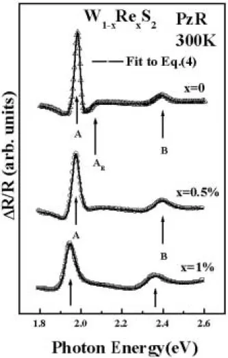
Figure 5. The PzR spectra of the W1-xRexS2 single crystals at 300 K. The solid curves are the least-squares fits using equation (4). Arrows under the curves show the peak positions of the two interband excitonic features, A and B, respectively. The antiresonance feature denoted AR for WS2 is also indicated.
V Figure 6. FESEM images of the vertically aligned IrO2 nanotubes grown on the sapphire(100) substrate.
(a) and (b) top view; (c) perspective view; (d) and (e) cross view.
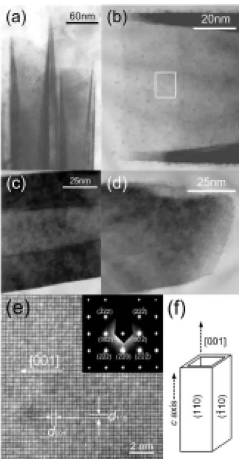
Figure 7. TEM images of the IrO2 nanotubes focused on (a) two individual tubes; (b) the front end; (c) the middle; (d) the bottom. (e) The high-resolution TEM image and its SAD pattern taken from the tube-wall in 5.3(b). (f) A schematic diagram of the IrO2 nanotube.
Figure 8. FESEM images of the well aligned IrO2 nanotubes grown on LiTaO3 (012) substrate. (a) and (b) top view; (c) cross view; (d) focus on a typical IrO2 nanotube.
Figure 9. (a) The cross-sectional TEM image of the IrO2 nanotubes on LiTaO3(012) substrate, and its corresponding SAD patterns taken separately from the regions of (b) IrO2 nanotubes, (c) LiTaO3 substrate and (d) interface along the zone axes of IrO2 [ 111 ] and LiTaO3 [221] . (e) The schematic diagram of the orientation relationship between the nanotube and substerate.
VI