超薄電漿氮化氧化層與高介電常數氧化鉿於閘極介電層之研究
170
0
0
全文
(2) 超薄電漿氮化氧化層與高介電常數氧化鉿於閘極 介電層之研究. Study on Ultrathin Plasma Nitrided Oxide and HfO2 High-κ Gate Dielectrics 研 究 生: 彭 辭 修. Student: Tsu-Hsiu Perng. 指導教授: 張 俊 彥 博士. Advisor: Dr. Chun-Yen Chang. 國 立 交 通 大 學 電子工程學系 電子研究所 博 士 論 文 A Dissertation Submitted to the Institute of Electronics College of Electrical Engineering and Computer Science National Chiao Tung University in Partial Fulfillment of the Requirements for the Degree of Doctor of Philosophy in Electronics Engineering June 2005 Hsinchu, Taiwan, Republic of China. 中 華 民 國. 九 十 四. 年. 六. 月.
(3) 超薄電漿氮化氧化層與高介電常數氧化鉿於閘極 介電層之研究 研 究 生: 彭 辭 修. 指導教授: 張 俊 彥 博士. 國 立 交 通 大 學. 電子工程學系 電子研究所. 摘要. 在以超薄電漿氮化氧化層作為閘極介電層的 N 型金氧半場效電晶體中,由通 道熱電子與基板熱電子注入而引起的元件劣化效應是本論文研究的主題之一。相 較於一般傳統使用的熱氧化層,可以發現超薄氮化閘極介電層比較容易受到通道 熱電子與基板熱電子效應的影響,導致更大的臨界電壓偏移與轉移電導值降低。 劣化增加的嚴重性會隨著在閘極介電層因氮化時間增長所致的氮元素含量增加而 增加。儘管對於傳統的熱氧化層或是電漿氮化氧化層二者而言,由基板熱電子所 引起的劣化是與注入電子的能量強烈相關,但是氮化氧化層表現在臨界電壓偏移 的明顯劣化情況卻是發生於較熱氧化層為低的基板偏壓值。在以電漿氮化氧化層 作為閘極介電層的 N 型金氧半場效電晶體中,這種經由基板負偏壓致使的劣化增 加現象,可歸因於在電漿氮化製程程序中導入的一個較高濃度的順磁性電子陷阱 先驅物。另一方面,在以超薄電漿氮化氧化層作為閘極介電層的 P 型金氧半場效 i.
(4) 電晶體元件中,也可以發現類似的劣化趨勢。在通道熱電子壓迫測試之後,可以 發現更嚴重的臨界電壓偏移與轉導值降低現象。不過,氮化氧化層作為閘極介電 層的 P 型金氧半場效電晶體,會受到相較於傳統熱氧化層為大的負偏壓溫度不穩 定效應。這種由於受偏壓與溫度壓迫測試導致的不穩定現象,在 N 型金氧半場效 電晶體元件中是不顯著的。. 本論文探討的另一個主題是氧化鉿,一個作為金氧半場效電晶體閘極介電層 的最佳高介電常數材料。在金絕半電容器的製作中,採用原子汽相沉積氧化鉿介 電層,搭配以濺鍍方式沉積銅或鋁金屬作為閘極所組成的。為了便於比較,同時 也製作了以二氧化矽介電層所組成的金絕半電容器對照組。利用偏壓溫度壓迫測 試與崩潰電荷測試方法,可以對電容器的穩定性與可靠性進行檢驗。相對於在二 氧化矽介電層中的高漂移速率,銅金屬在氧化鉿介電層的組成中顯得相當穩定。 銅金屬閘極的氧化鉿電容器也具有比鋁金屬閘極較高的電容值,而且沒有可靠性 降低的問題。此實驗結果顯示具有高密度 9.68 g/cm3的氧化鉿是一個很好的阻擋銅 金屬擴散的阻障層。而這也意味著銅金屬在積體電路閘極介電層後續製程整合的 可行性。. 氧化鉿高介電常數材料的另一個重要應用是作為金絕金電容器的絕緣層。利 用一標準的後段金屬層作為下電極,金絕金電容器已經成為微處理器、高頻電路 與混合信號積體電路之一關鍵被動元件。為了增加電路密度與減少晶胞面積與成 本,高電容密度是金絕金電容器一項很重要的考量因素。因此採用高介電常數材 料像是氧化鉿,就是增加電容密度的一個很有效的方式。在金絕金電容器的實驗 結果可以得到約5×10⁻⁹ A/cm2的低漏電流密度與約3.4 fF/µm2的高電容密度,達到很 小的溫度係數與頻散效應。一些不同的金屬電極像是鉭、鋁、銅等也加以比較。 最後氧化鉿金絕金電容器的電性傳導機制可被推導出來並歸類為Frenkel-Poole形 式。. ii.
(5) Study on Ultrathin Plasma Nitrided Oxide and HfO2 High-κ Gate Dielectrics Student: Tsu-Hsiu Perng. Advisor: Dr. Chun-Yen Chang. Department of Electronics Engineering and Institute of Electronics College of Electrical Engineering and Computer Science National Chiao Tung University. Abstract. The degradation induced by channel hot electron (CHE) and substrate hot electron (SHE) injection in nMOSFETs with ultrathin plasma nitrided gate dielectric was studied in this thesis. Compared to the conventional thermal oxide, the ultrathin nitrided gate dielectric is found to be more vulnerable to CHE and SHE stress, resulting in enhanced threshold voltage shift and transconductance reduction. The severity of the enhanced degradation increases with increasing nitrogen content in gate dielectric with prolonged nitridation time. While the SHE-induced degradation is found to strongly relate to the injected electron energy for both conventional oxide and plasma-nitrided oxide, dramatic degradation in threshold voltage shift for nitrided oxide is found to occur at a lower substrate bias magnitude, compared to thermal oxide. This enhanced degradation by negative substrate bias in nMOSFETs with plasma-nitrided gate dielectric is attributed to a higher concentration of paramagnetic electron trap precursors introduced iii.
(6) during plasma nitridation. On the other hand, similar degradation trend was also found in the pMOSFET devices with ultrathin plasma nitrided gate dielectric. Enhanced threshold voltage shift and transconductance reduction were observed after CHE stress for the nitrided devices. Nevertheless, the pMOSFETs with nitrided gate dielectric suffer larger negative bias temperature instability (NBTI), comparing to that with conventional thermal oxide. Such instability owing to bias-temperature stressing is inconspicuous in nMOSFET devices.. The other subject included in this thesis is HfO2, a promising high-k material in gate dielectric of MOSFETs. Metal-insulator-semiconductor (MIS) capacitors were fabricated using atomic vapor deposition (AVD) HfO2 dielectric with sputtered copper and aluminum gate electrodes. The counterparts with SiO2 dielectric were also fabricated for comparison. Bias-temperature stress (BTS) and charge-to-breakdown (QBD) test were conducted to examine the stability and reliability of these capacitors. In contrast with the high Cu drift rate in SiO2 dielectric, Cu in contact with HfO2 seems to be very stable. The HfO2 capacitors with Cu-gate also depict higher capacitance without showing any reliability degradation, compared to the Al-gate counterparts. These results indicate that HfO2 with its considerably high density of 9.68 g/cm3 is acting as a good barrier to Cu diffusion, and it thus appears feasible to integrate Cu metal with the post-gate-dielectric ULSI manufacturing processes.. Another application for HfO2 high-k dielectrics is metal-insulator-metal (MIM) capacitors. MIM capacitors using one of the standard back-end metal layers as bottom electrode have emerged as key passive components for microprocessors, high frequency circuits, and mixed-signal integrated circuits applications. A high capacitance density is important for a MIM capacitor to increase the circuit density and reduce the cell area. iv.
(7) and cost. Therefore, adoption of high-k material like HfO2 is a very efficient way to increase the capacitance density. Experimental results show low leakage current densities of ~5×10⁻⁹ A/cm2 and high capacitance density of ~3.4 fF/µm2 at 100 kHz in the MIM capacitors. The temperature coefficient and frequency dispersion effect for these MIM capacitors were very small. Different metal electrodes like tantalum, aluminum, and copper were also investigated and compared. Finally, the mechanism of electrical transport was extracted for the HfO2 MIM capacitors to be Frenkel-Poole type conduction mechanism.. v.
(8) 誌. 謝. 首先,我要向我的指導教授張俊彥校長致上最高的敬意與謝意。 感謝老師在這些年的學習生涯中給予我極大的研究空間及支持,使我 能順利的完成博士學位,同時從他身上也習得許多待人處世應對進退 之道及其對知識追求的積極態度。老師除了在學術專業上的創新遠見 讓我受益無窮外,不忮不求的學者風範更深深影響我們。老師能夠於 學術上一再受到海內外給予最高榮譽肯定,不啻對於台灣半導體領 域,更對國家高等教育與經營管理上都有卓越的貢獻。 其次,要感謝的人是即將至電子工程學系任教的簡昭欣博士。在 實驗研究方面,受到簡博士非常多的指導與點悟,豐厚的學術涵養是 在無涯學海中引導我的一盞明燈,而在平常生活方面則是敦促我不斷 成長的學長。這些年來受到他在各方面的指導及照顧甚多,儘管凡事 不能盡如人意,但虔誠向佛的他,總是能夠在遇到挫折時以心靈導師 的身分教導以淡然處之,給予適切的鼓勵。 再者一位要特別感謝的是實驗室的學長,陳經緯博士。從一開始 的聯電合作計畫、台積電合作計畫到國家奈米元件實驗室的研究,雖 然不是很順遂,但學長都是以一拓荒先鋒者的姿態,披荊斬棘,克服 萬難,引領學弟向前挺進。孜孜不倦的求學精神與嚴謹的治學態度, 一直是學弟們奉為圭臬的準則。廣博的學識與豐富的人生經驗,是我 vi.
(9) 們時常請益的百科全書。 另外要感謝黃調元教授,其專業素養與謙恭處世的儒者風範是我 等後輩學習景仰的目標。行雲流水般的英文寫作造詣是可望而不可企 及的標竿,不計代價與無私的辛勞幫助我們論文投稿的修改與潤飾。 感謝中山大學物理系的張鼎張教授、交通大學顯示所的劉柏村教授, 於論文投稿方面的諸多建議。 再來要感謝國家奈米元件實驗室的正傑學長、明瑞、世祿等在實 驗樣品與分析的製備協助。很幸運地可以與雅嫃、宇駿、凱立、怡誠、 慶宗、兆欽等快速電子實驗室的學弟妹於此領域中接受簡博士的薰 陶。一同在加州土地上迷路漫遊的宗鳴、紀文等學弟,曾經在飛鳳山 的山徑上汗流浹背的峻豪、聖懿、道諺、立偉等學弟。還有快速電子 實驗室的師道學長,宗熺、宗霖、文政、丁勇、漢譽、永俊、心卉、 武陵、哲育、……等學弟妹以及伊喬等歷任助理們在這些年來,不論 是在日常生活或實驗上的互相砥礪、關懷與扶持。 從一個初踏入交通大學的新鮮人,如今即將邁向人生另一個階 段。感謝父母從小含辛茹苦的扶養與對我教育的重視,無虞匱乏的支 持鼓勵,成就我今天的小小成就,謹將這份成果獻給我摯愛的家人。. vii.
(10) Contents Abstract (Chinese) ............................................................................................................... i Abstract (English) .............................................................................................................. iii Acknowledgement ............................................................................................................. vi Contents ........................................................................................................................... viii Table Captions .................................................................................................................... xi Figure Captions ................................................................................................................. xii. Chapter 1 Introduction 1.1 Overview of Ultrathin Gate Oxide Reliability .................................................... 1 1.2 Challenge of Gate Dielectric Scaling .................................................................. 3 1.3 Scope and Organization of the thesis .................................................................. 6. Chapter 2 Trends in Gate Oxide Scaling 2.1 MOSFET Scaling .............................................................................................. 10 2.2 Recent Gate Oxide Scaling Trends ................................................................... 12 2.2.1 Gate Leakage and Static Power Dissipation ........................................... 12 2.2.2 Scaling Limit of SiO2 ............................................................................. 14 2.3 High-k Gate Dielectrics ..................................................................................... 15 2.3.1 Target Dielectric Constant ...................................................................... 17 2.3.2 Bandgap and Band Offsets ..................................................................... 20 2.3.3 Si Interface Properties ............................................................................ 21 2.4 Zirconium and Hafnium Silicates ..................................................................... 23 2.5 Summary ........................................................................................................... 26 viii.
(11) Chapter 3 Reliability of Ultrathin Plasma Nitrided Gate Oxides for ULSI Devices 3.1 Backgrounds and Motivation ............................................................................ 32 3.2 Experimental Procedure .................................................................................... 33 3.3 Electrical Characteristics of Plasma Nitrided Gate Oxides ............................... 34 3.4 Channel Hot Carrier Degradation ...................................................................... 35 3.5 Enhanced Negative Substrate Bias Degradation ............................................... 38 3.6 Conclusions ....................................................................................................... 40. Chapter 4 Reliability of pMOSFETs with Ultrathin Plasma Nitrided Gate Dielectric 4.1 Backgrounds and Motivation ............................................................................ 61 4.2 Experimental Procedure .................................................................................... 63 4.3 PMOSFETs with Ultrathin Plasma Nitrided Gate Dielectric ............................ 64 4.4 Channel Hot Hole Degradation ......................................................................... 65 4.5 Enhanced Negative Bias Temperature Instability .............................................. 66 4.6 Conclusions ....................................................................................................... 68. Chapter 5 MIS Capacitors with HfO2 Dielectrics 5.1 Background and Motivation .............................................................................. 82 5.2 Sample Preparation ............................................................................................ 83 5.3 Material Analysis of HfO2 Dielectric Film ........................................................ 84 5.3.1 TEM Analysis .......................................................................................... 84 5.3.2 Optical Analysis ...................................................................................... 85 5.3.3 Surface Analysis ...................................................................................... 86 5.4 Electrical Characterization of HfO2 Capacitors with Pt Electrode .................... 87 5.5 HfO2 MIS Capacitor with Copper Gate Electrode ............................................ 88 ix.
(12) 5.5.1 Motivation of Incorporating Copper Gate Electrode .............................. 88 5.5.2 Experimental Procedure ......................................................................... 88 5.5.3 Capacitor Characterization and Bias Temperature Stressing .................. 89 5.5.4 Constant Current Stress and Charge-to-Breakdown ............................... 90 5.6 Conclusions ....................................................................................................... 92. Chapter 6 Investigation of HfO2 Dielectrics for Inter-Poly Dielectrics and Metal-Insulator-Metal Capacitors 6.1 Introduction ..................................................................................................... 107 6.2 Experimental Procedure .................................................................................. 108 6.3 Comparison of Inter-Poly Dielectrics and Metal-Insulator-Metal Capacitors . 110 6.4 Metal-Insulator-Metal Capacitors with HfO2 Dielectric .................................. 111 6.4.1 High-Density MIM Capacitors with HfO2 Dielectric ............................ 111 6.4.2 Thermal Stress on the MIM Capacitors ................................................. 112 6.4.3 Leakage Mechanism of the MIM Capacitors ........................................ 113 6.5 Conclusions ...................................................................................................... 114. Chapter 7 Conclusions and Suggestions for Future Work 7.1 Conclusions of This Study .............................................................................. 124 7.2 Suggestions for Future Work .......................................................................... 126. References ................................................................................................................... 127 Vita ................................................................................................................................ 148 Publication List ......................................................................................................... 149. x.
(13) Table Captions Chapter 2 Table 2.1. Projected transistor parameters for future technology generations.. Table 2.2. Selected excerpts from the 2004 update of the International Technology Roadmap for Semiconductors.. Chapter 6 Table 6.1. Voltage linearity coefficients α (ppm/V2) and β (ppm/V) as a function of frequency for the HfO2 MIM capacitors with Ta, Al, and Cu top electrode.. xi.
(14) Figure Captions Chapter 1 Fig. 1.1. LSTP logic scaling-up of gate leakage current density limit and of simulated gate leakage due to direct tunneling. [ITRS 2003]. Fig. 1.2. Polysilicon depletion effects. Chapter 2 Fig. 2.1. (a) The MOSFET ideally acts as a 3-terminal switch. (b) Practical realization of the MOSFET requires a gate capacitor.. Fig. 2.2. (a) Simplified band diagram of the MOS system. (b) Direct tunneling of carriers through the insulator potential barrier can occur for thin dielectric layers.. Fig. 2.3. Extrapolated gate oxide scaling trend for recent CMOS technologies.. Fig. 2.4. Extrapolated trend of active and leakage power dissipation for state-of-the-art CMOS technologies.. Fig. 2.5. Plot of bandgap versus static dielectric constant for representative high-k gate dielectric materials.. Fig. 2.6. Diagram illustrating a high-k gate dielectric stack with a low-k interfacial layer.. Fig. 2.7. (a) A gate dielectric stack formed of a high-k layer and a low-k interfacial layer. (b) A stack formed of a single, uniform layer with intermediate k-value. Both stacks provide 1.0 nm EOT.. Chapter 3 Fig. 3.1. Typical Id-Vd characteristics for (a) long channel (W/L = 10/10 µm) and (b) xii.
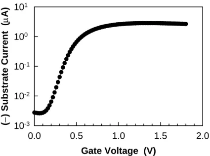
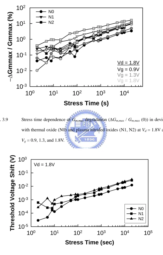
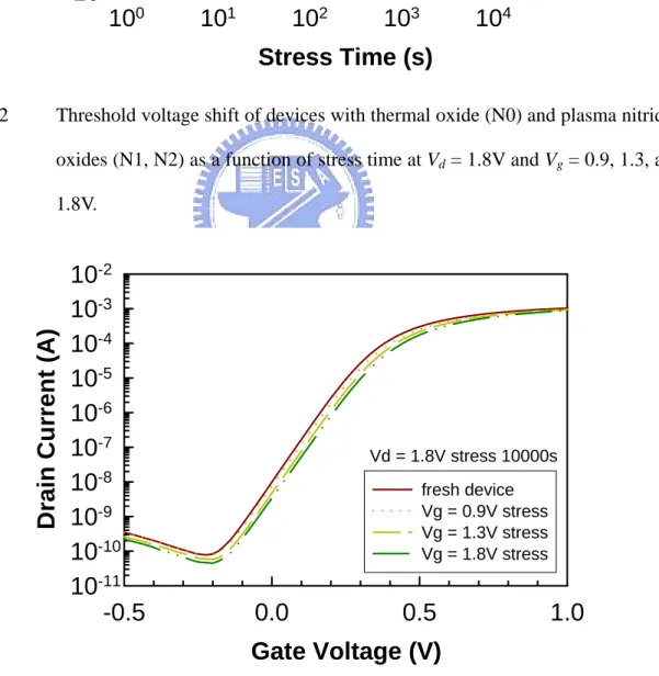
(15) deep submicron (W/L = 10/0.13 µm) devices with thermal oxide (N0) and plasma nitrided oxides (N1, N2). Fig. 3.2. Typical Id-Vg characteristics for (a) long channel (W/L = 10/10 µm) and (b) deep submicron (W/L = 10/0.13 µm) devices with thermal oxide (N0) and plasma nitrided oxides (N1, N2).. Fig. 3.3. Drain current (Id) as a function of effective gate drive (Vg − Vt) for (a) long channel (W/L = 10/10 µm) and (b) deep submicron (W/L = 10/0.13 µm) devices with thermal oxide (N0) and plasma nitrided oxides (N1, N2).. Fig. 3.4. Gm-Vg characteristics for (a) long channel (W/L = 10/10 µm) and (b) deep submicron (W/L = 10/0.13 µm) devices with thermal oxide (N0) and plasma nitrided oxides (N1, N2).. Fig. 3.5. Gm * Tox as a function of effective gate drive (Vg − Vt) for (a) long channel (W/L = 10/10 µm) and (b) deep submicron (W/L = 10/0.13 µm) devices with thermal oxide (N0) and plasma nitrided oxides (N1, N2).. Fig. 3.6. Stress time dependence of Gm,max degradation (∆Gm,max / Gm,max(0)) in devices with thermal oxide (N0) and plasma nitrided oxides (N1, N2) at (a) Vd = 1.8V, Vg = Isub,max, (b) Vd = 2.0V, Vg = Isub,max, and (c) Vd = 2.2V, Vg = Isub,max.. Fig. 3.7. Typical substrate current curve as a function of gate voltage to estimate the stressing condition.. Fig. 3.8. Stress time dependence of Gm,max degradation (∆Gm,max / Gm,max (0)) in devices with thermal oxide (N0) and plasma nitrided oxides (N1, N2) at (a) Vd = 1.8V, Vg = 0.9V and (b) Vd = Vg = 1.8V.. Fig. 3.9. Stress time dependence of Gm,max degradation (∆Gm,max / Gm,max (0)) in devices with thermal oxide (N0) and plasma nitrided oxides (N1, N2) at Vd = 1.8V and Vg = 0.9, 1.3, and 1.8V.. Fig. 3.10. Threshold voltage shift of devices with thermal oxide (N0) and plasma nitrided xiii.
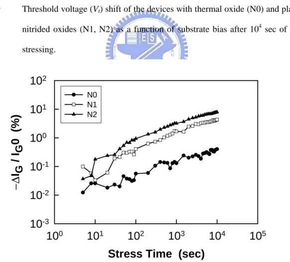
(16) oxides (N1, N2) as a function of stress time at (a) Vd = 1.8V, Vg = Isub,max, (b) Vd = 2.0V, Vg = Isub,max, and (c) Vd = 2.2V, Vg = Isub,max. Fig. 3.11. Threshold voltage shift of devices with thermal oxide (N0) and plasma nitrided oxides (N1, N2) as a function of stress time at (a) Vd = 1.8V, Vg = 0.9V and (b) Vd = Vg = 1.8V.. Fig. 3.12. Threshold voltage shift of devices with thermal oxide (N0) and plasma nitrided oxides (N1, N2) as a function of stress time at Vd = 1.8V and Vg = 0.9, 1.3, and 1.8V.. Fig. 3.13. Id-Vg characteristics of device with plasma nitrided oxide (N2) before and after 10,000 sec stressing at Vd = 1.8V, Vg = 0.9, 1.3, and 1.8V.. Fig. 3.14. Stress time dependence of Gm,max degradation (∆Gm,max / Gm,max (0)) in devices with thermal oxide (N0) and plasma nitrided oxides (N1, N2) at (a) Vg = 1.8V, Vd = Vs = Vb = 0V and (b) Vg = 1.8V, Vb = −2V, Vd = Vs = 0V.. Fig. 3.15. Threshold voltage shift of devices with thermal oxide (N0) and plasma nitrided oxides (N1, N2) as a function of stress time at (a) Vg = 1.8V, Vd = Vs = Vb = 0V and (b) Vg = 1.8V, Vb = −2V, Vd = Vs = 0V.. Fig. 3.16. (a) Gm,max degradation (∆Gm,max / Gm,max (0)) and (b) threshold voltage shift of devices with thermal oxide (N0) and plasma nitrided oxides (N1, N2) as a function of stress time at Vg = 2.2V, Vd = Vs = Vb = 0V.. Fig. 3.17. Stress time dependence of (a) Gm,max degradation (∆Gm,max / Gm,max (0)), (b) threshold voltage shift, and (c) drain current degradation (∆Id / Id(0)) in devices with thermal oxide (N0) and plasma nitrided oxides (N1, N2) at Vg = 2.2V, Vb = −2V, Vd = Vs = 0V.. Fig. 3.18. Substrate hot electron (SHE) stress time dependence of (a) relative Gm degradation and (b) threshold voltage (Vt) shift for devices with thermal oxide (N0) and plasma nitrided oxides (N1 and N2). Substrate biases are 0V xiv.
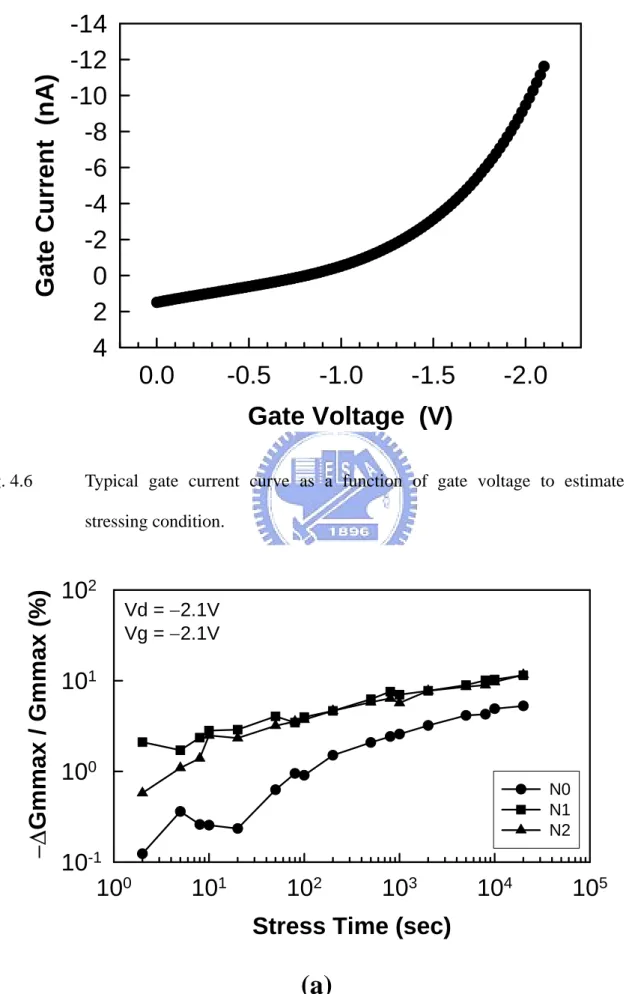
(17) and –2V. Fig. 3.19. Threshold voltage (Vt) shift of the devices with thermal oxide (N0) and plasma nitrided oxides (N1, N2) as a function of substrate bias after 104 sec of SHE stressing.. Fig. 3.20. Relative gate leakage current change as a function of SHE stress time for different samples.. Chapter 4 Fig. 4.1. Typical Id-Vd characteristics for (a) long channel (W/L = 10/10 µm) and (b) deep submicron (W/L = 10/0.13 µm) devices with thermal oxide (N0) and plasma nitrided oxides (N1, N2).. Fig. 4.2. Typical Id-Vg characteristics for (a) long channel (W/L = 10/10 µm) and (b) deep submicron (W/L = 10/0.13 µm) devices with thermal oxide (N0) and plasma nitrided oxides (N1, N2).. Fig. 4.3. Drain current (Id) as a function of effective gate drive (Vg − Vt) for (a) long channel (W/L = 10/10 µm) and (b) deep submicron (W/L = 10/0.13 µm) devices with thermal oxide (N0) and plasma nitrided oxides (N1, N2).. Fig. 4.4. Gm-Vg characteristics for (a) long channel (W/L = 10/10 µm) and (b) deep submicron (W/L = 10/0.13 µm) devices with thermal oxide (N0) and plasma nitrided oxides (N1, N2).. Fig. 4.5. Gm * Tox as a function of effective gate drive (Vg − Vt) for (a) long channel (W/L = 10/10 µm) and (b) deep submicron (W/L = 10/0.13 µm) devices with thermal oxide (N0) and plasma nitrided oxides (N1, N2).. Fig. 4.6. Typical gate current curve as a function of gate voltage to estimate the stressing condition.. Fig. 4.7. Stress time dependence of Gm,max degradation (∆Gm,max / Gm,max (0)) in devices xv.
(18) with thermal oxide (N0) and plasma nitrided oxides (N1, N2) at (a) Vd = Vg = −2.1V, (b) Vd = Vg = −2.3V, and (c) Vd = Vg = −2.5V. Fig. 4.8. Comparison of the gate current curves as a function of gate voltage biasing at Vd = Vg = −2.5 V.. Fig. 4.9. Threshold voltage shift of devices with thermal oxide (N0) and plasma nitrided oxides (N1, N2) as a function of stress time at (a) Vd = Vg = −2.1V, (b) Vd = Vg = −2.3V, and (c) Vd = Vg = −2.5V.. Fig. 4.10. Stress time dependence of Id degradation (∆Id / Id (0)) in devices with thermal oxide (N0) and plasma nitrided oxides (N1, N2) at (a) Vd = Vg = −2.1V, (b) Vd = Vg = −2.3V, and (c) Vd = Vg = −2.5V.. Fig. 4.11. Schematic plot of experimental configuration for NBTI stress.. Fig. 4.12. Threshold voltage shift of devices with thermal oxide (N0) and plasma nitrided oxides (N1, N2) as a function of stress time at (a) under NBTI stress (Vg = −2.5V, T = 125°C) and (b) Vg = −2.5V.. Fig. 4.13. Threshold voltage shift of devices with thermal oxide (N0) and plasma nitrided oxides (N1, N2) as a function of stress time under NBTI stress.. Chapter 5 Fig. 5.1. Thickness of HfO2 film as a function of deposition time before and after O2 and N2 ambient annealing.. Fig. 5.2. TEM picture of HfO2 film deposited by PVD (a) with the power of 100 W for 300 sec, (b) with higher resolution. The PDA condition is 800°C in O2 ambient for 30 sec.. Fig. 5.3. (a) TEM picture of Pt/HfO2/Si deposited by PVD. (b) TEM picture of Pt/HfO2/Si deposited by PVD with higher resolution.. Fig. 5.4. Reflectance spectra of thin HfO2 films on Si. xvi.
(19) Fig. 5.5. (a) XPS spectrum shows a typical HfO2 chemical bonding. (b) XPS spectra show HfO2 chemical bonding after elevated temperature annealing.. Fig. 5.6. AFM image of HfO2 on p-Si, the RMS roughness is about 0.14 nm.. Fig. 5.7. C-V curves of a thin-film HfO2 capacitor with Pt electrode on n-Si substrate.. Fig. 5.8. Schematic representation of an HfO2 capacitor with Pt electrode on n-Si substrate.. Fig. 5.9. 100 kHz curves of both positive and negative C-V sweeps. The hysteresis is less than 110 mV.. Fig. 5.10. I-V curves for the film shown in Fig. 5.9.. Fig. 5.11. C-V curves of (a) Cu/SiO2/Si and Al/SiO2/Si capacitors, (b) Cu/HfO2/Si and Al/HfO2/Si capacitors before and after BTS at 150°C for 1000 sec. The applied field was +1 MV/cm.. Fig. 5.12. (a) Typical I-V curves of Cu/HfO2/Si capacitors before and after BTS at 150°C for 1000 sec. (b) Typical gate current and substrate current variation curves of Cu/HfO2/Si capacitors during BTS. The applied field was +1 MV/cm.. Fig. 5.13. Typical C-V curves of Cu/HfO2/Si capacitors at frequencies varies from 1 kHz to 1 MHz.. Fig. 5.14. VFB shifts of Cu/SiO2/Si, Al/SiO2/Si, Cu/HfO2/Si, and Al/HfO2/Si capacitors after BTS test at +1 MV/cm for 1000 sec. The temperatures were varied from 100 to 200°C.. Fig. 5.15. Typical I-V curves of HfO2 and SiO2 MIS capacitors.. Fig. 5.16. Gate voltage variation of SiO2 and HfO2 capacitors with Cu and Al gate electrodes subjected to CCS as a function of time.. Fig. 5.17. Gate voltage variation of (a) HfO2 and (b) SiO2 capacitors with Cu gate electrodes subjected to CCS as a function of time.. Fig. 5.18. Cumulative QBD plots of Cu/HfO2/Si, Al/HfO2/Si, Cu/SiO2/Si, and Al/SiO2/Si xvii.
(20) capacitors.. Chapter 6 Fig. 6.1. Current-voltage (J-V) characteristics of the IPD and MIM capacitors.. Fig. 6.2. Capacitance density of the MIM capacitor as a function of temperature at frequencies varied from 100Hz to 1MHz.. Fig. 6.3. Capacitance density of the IPD as a function of temperature at frequencies varied from 100Hz to 1MHz.. Fig. 6.4. Capacitance density of the IPD as a function of frequency at temperatures varied from 25°C to 200°C.. Fig. 6.5. Capacitance-voltage (C-V) characteristics of HfO2 MIM capacitors with Ta electrodes at the frequencies from 1 kHz to 1 MHz.. Fig. 6.6. Capacitance-voltage (C-V) characteristics of HfO2 MIM capacitors with Al, Ta, and Cu top electrodes at the frequency of 100 kHz.. Fig. 6.7. Current density-voltage (J-V) characteristics of the HfO2 MIM capacitors with the top electrodes of Al, Ta, and Cu.. Fig. 6.8. Loss tangent as a function of frequency for the MIM capacitors with Al, Ta, and Cu top electrodes.. Fig. 6.9. Capacitance density of the MIM capacitor with Ta top electrode as a function of frequency after thermal stress from 25°C to 125°C.. Fig. 6.10. Capacitance density of the MIM capacitor with Al and Cu top electrode as a function of frequency after thermal stress from 25°C to 125°C.. Fig. 6.11. Poole-Frenkel plot showing the current density versus electric field characteristics at five measurement temperatures from 25°C to 125°C for HfO2 MIM capacitor with (a) Ta, (b) Al, and (c) Cu top electrode.. xviii.
(21) Chapter 1 Introduction. 1.1. Overview of Ultrathin Gate Oxide Reliability The IC industry has been rapidly and consistently scaling the design rule, increasing the. chip and wafer size, and cleverly improving the design of devices and circuits for over 35 years. As a result, the industry has enjoyed exponential increases in chip speed and functional density versus time combined with exponential decreases in power dissipation and cost per function versus time, as projected by Moore’s Law [1]-[3]. As metal-oxide semiconductor field-effect transistors (MOSFETs) are scaled to deep submicron dimensions, the integrated circuit (IC) industry is running into increasing difficulties in continuing to scale at the accustomed rate, owing to the small dimensions and certain key device, material, and process limits that are being approached.. For the past three decades, CMOS technology has powered a revolution and leads the industry to enjoy a great success due to its highly integrated performance in both dimension and density with scaling. The great advances made in ULSI technology in recent years have been underpinned by rapid developments in the design and fabrication of CMOS devices. It is often said that the real magic in silicon technology lies not in the silicon crystalline material but in silicon dioxide, since silicon dioxide is employed as many critical components of silicon devices [4]. Due mainly to formation of nearly perfect interface property of silicon and silicon dioxide, SiO2 has been treated as an ideal gate insulator of MOS devices for several. 1.
(22) generations. However, as CMOS technology scales aggressively into deep submicron regime and beyond, gate oxide reliability becomes of a critical issue. Though physical gate length is the most important factor in scaling CMOS transistor density and performance, aggressive scaling of gate oxide thickness is required. For a MOSFET to behave as a transistor, the gate must exert greater control over the channel than the drain dose, i.e., the gate to channel capacitance must be larger than the drain to channel capacitance [5]. Furthermore, scaling of gate oxide thickness not only benefits the driving capability of transistor but suppresses the short channel effect, which is known as a stumbling stone for CMOS scaling. Therefore, to ensure the continued shrinkage of CMOS technologies down to deep submicron regime and beyond, ultrathin gate dielectric with low defect density and high reliability is indispensable.. Since Momose et al. from Toshiba group first proposed the use of 1.5 nm direct-tunneling gate oxide for nMOSFETs with extremely high device performance in 1994 [6], many aggressive studies regarding direct tunneling gate oxide for sub-quarter micron devices have been carried out [7]-[14]. The application of direct-tunneling gate oxide not only achieves high speed for logic circuits, its use is also essential for high-performance RF applications [13], [14]. In addition, the use of thinner oxides is also critical to meet the demands of lower programming voltage for future nonvolatile memories [15]. However, the application of direct-tunneling gate oxide to ULSI devices faces many challenges. Firstly, the presence of large quantum-mechanical (QM) tunneling current is a serious scaling limitation in terms of standby power consumption [16]. Secondly, breakdown characteristics for ultrathin oxides become even more critical due to the dramatic increase in electric field across the oxide during normal device operation. Whether oxide becomes inherently more robust or more vulnerable to electric stress as it thins down therefore plays a very crucial role for its applications to ULSI devices. Thirdly, poly-gate depletion effects are known to get worse with oxide scaling. This is because the operating gate voltage normally does not scale 2.
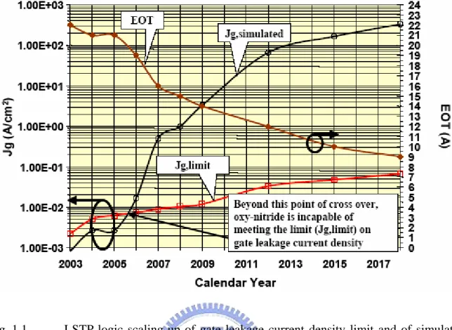
(23) proportionally to the oxide thickness, and therefore the average surface field increases. The additional voltage drop at the poly depletion layer results in undesirable drive current degradation [17]. Since these effects worsen for thinner oxides, it could become a limiting factor for future device scaling.. A number of difficult challenges for MOSFET scaling are pointed out in the 2003 ITRS, and these are exacerbated by the previously mentioned rapid scaling. These challenges include several that are the result of the scaling down of the gate dielectric thickness: excessive gate leakage current, boron penetration from the p+ polysilicon gate electrode into the channel of the MOSFET, and increasing deleterious impact of polysilicon depletion in the polysilicon gate electrodes. Also, with scaling, the mobility of electrons and holes in the inversion layer is projected to become inadequate to meet the transistor performance goals. Finally, the classical planar bulk MOSFET itself will likely eventually become inadequate to meet transistor requirements, mainly because of the inability to adequately control short-channel and quantum effects and statistical variability for very small transistors.. 1.2. Challenge of Gate Dielectric Scaling As discussed in the previous section, the challenge inherent is associated with the rapid. scaling of the gate dielectric thickness, Td for high-performance and low-power logic technologies. The first difficulty is a susceptibility to boron penetration, which is the uncontrolled diffusion of boron from the heavily doped p+ poly gate of the pMOSFETs through the thin gate dielectric and into the MOSFET channel. The result is an uncontrollable but positive shift in the pMOSFET Vt. Lightly doping the gate oxide with nitrogen to form oxy-nitride generally controls this problem [18] and is the standard approach for current 3.
(24) leading-edge IC technologies. The other major difficulty is excessive gate leakage current, as the oxy-nitride becomes very thin with scaling. The predominant conduction mode for very thin dielectrics is direct tunneling, where the gate leakage current increases exponentially with decreasing dielectric thickness. In Figure 1.1 [2], the 2003 ITRS projections for EOT and Jg, limit. are plotted for low-standby-power (LSTP) logic. Also plotted are simulations of the. expected gate leakage current density assuming the gate dielectric is oxy-nitride. As indicated in the figure, by 2006 oxy-nitride is incapable of satisfying the limit (Jg, limit) on gate leakage current density. Carrying out a similar analysis for low-operating-power (LOP) and high-performance logic, oxy-nitride is incapable of satisfying the limit on gate leakage current density by 2006 for LOP logic also, and by 2007 for high-performance logic [2].. In 2006 or 2007, when oxy-nitride gate dielectric becomes incapable of meeting the maximum gate leakage limit, the preferred approach to reducing gate leakage in order to satisfy the limit is to replace the oxy-nitride with a “high-κ” dielectric. Such a dielectric has a significantly higher relative dielectric constant k than the kox = 3.9 value of silicon dioxide (the k for lightly nitrogen doped oxy-nitride is also close to 3.9). For a dielectric of thickness Td, the equivalent oxide thickness, EOT, is:. EOT = Td / (k / kox) = Td / (k / 3.9).. (1.1). To first order, a transistor with such a gate dielectric has a gate capacitance per unit area,. Cg, area = kε0 / Td = koxε0 / EOT,. (1.2). where ε0 is the dielectric constant of vacuum. koxε0/EOT is also the value of the gate capacitance per unit area for an otherwise identical transistor with a silicon dioxide gate dielectric of thickness EOT. Hence, to first order, the major electrical characteristics such as. 4.
(25) Ion should be the same for both transistors (except the gate leakage current, which should be significantly reduced for the transistor with high-κ gate dielectric). For silicon dioxide, with k = 3.9, EOT = Td, while for high-κ gate dielectric, where k > 3.9, Td is significantly larger than EOT. Since direct tunneling is strongly dependent on Td, the gate leakage current density will generally be significantly smaller for the high-κ gate dielectric, if the energy barrier between the dielectric and silicon is large enough [19]. Extending current approaches using lightly nitrogen-doped oxy-nitride with k ~ 3.9, heavily nitrogen doped oxy-nitride has been shown to have k > 5, and as a result, gate leakage current reduced by more than an order of magnitude relative to silicon dioxide [20]. In simulating the gate leakage of oxy-nitride dielectric, as in Figure 1.1, such extended, heavily nitrogen doped oxy-nitride is assumed. Per the analysis above, high-κ gate dielectric is projected to be needed for low-power logic in 2006 and for high-performance logic in 2007. Very active research and development is being carried out on high-κ materials for the gate dielectric, and the current leading candidates are hafnium oxide, hafnium silicate, and hafnium oxy-nitride [21].. Another major front-end issue is polysilicon depletion in the gate electrode. When gate voltage is applied to turn on a MOSFET, a depletion region of thickness Wd forms adjacent to the polysilicon-oxide interface (see Figure 1.2). This depletion region increases the effective electrical thickness of the gate dielectric in inversion, EOTelec:. EOTelec = EOT + ∆poly = EOT + (kox / kSi)Wd ~ EOT + Wd / 3,. (1.3). where kSi = 11.9 is the relative dielectric constant of silicon and ∆poly encapsulates the impact of polysilicon depletion. According to Wilk et al. [19], ∆poly can be as much as 0.4 nm. As a result of the polysilicon depletion, EOT is replaced by EOTelec in (1.2) for the gate capacitance per unit area, reducing the capacitance. Consequently, for any given gate voltage, the inversion layer charge and Ion are reduced. The impact of polysilicon depletion becomes more 5.
(26) severe with the smaller EOT in succeeding technology generations. Increased doping of the polysilicon reduces the depletion, since Wd is inversely proportional to the square root of the polysilicon doping. However, with the limited solubility of the dopants, particularly boron for the p+ polysilicon gate of the pMOSFET, this solution will eventually become inadequate, even if germanium-doped polysilicon, which has higher solid solubility for boron, is used [22]. The preferred solution is metal-gate electrodes, since with metal gates there is virtually no depletion, no boron penetration, and sheet resistance is very low. According to 2003 ITRS projections, metal-gate electrodes will need to be implemented for high-performance logic by 2007 [2]. However, CMOS optimization requires a work function ~ 5.0 eV (near the silicon valence band edge) for pMOSFETs and ~ 4.1 eV (near the silicon conduction band edge) for nMOSFETs [23] to set the desired symmetric threshold voltages of 0.2 to 0.5 V for NMOS and −0.2 to −0.5 V for PMOS. One approach involves utilizing different metals with different work functions, one for the pMOSFET [24], [25], and one for the nMOSFET [26], [27] device. This would present difficult process integration problems and would tend to increase the chip processing complexity and cost. An alternative approach that aims to reduce the process complexity and cost is to utilize one material system for both metal electrodes, and use doping or alloy composition to vary the work function as necessary [25], [28].. 1.3. Scope and Organization of the thesis This thesis investigates promising candidates of alternative gate dielectrics containing. nitrided oxide and hafnium oxide.. The thesis is organized as follows:. 6.
(27) Chapter 2 reviews recent trends in gate oxide scaling to show that further scaling of SiO2 is limited by static power dissipation and other fundamental considerations. As an alternative to continuing to scale SiO2, the use of alternative high-k gate dielectrics is discussed. Several of the most important material properties for such high-k dielectrics are also reviewed.. Chapter 3 investigates the hot carrier injection reliability of nMOSFET’s with ultrathin plasma nitrided gate oxide. The devices with plasma nitrided oxide suffer more transconductance reduction and threshold voltage shift. The degradation is direct proportional to the plasma nitridation time. We report, for the first time, an enhanced degradation under negative substrate bias in nMOSFETs with ultrathin plasma nitrided gate dielectric. The enhanced degradation is attributed to the introduction of paramagnetic electron trap precursors during plasma nitridation.. Chapter 4 investigates the hot carrier injection reliability and negative bias temperature instability of pMOSFET’s with ultrathin plasma nitrided gate oxide. For channel hot-carrier stressing, the most efficient stressing condition is located corresponding to the region of maximum gate current. The negative threshold voltage shift indicates a positive charge build-up in the gate dielectric. For negative bias temperature stressing, appreciable enhancement of the threshold voltage shift can be observed through the raising of temperature. The enhanced device degradation is attributed to the H-related species and the interface trap generated during NBT stressing. NBTI is an important issue for pMOSFETs from the reliability point of view.. Chapter 5 presents the hafnium oxide film as alternative material to replace SiO2 for gate dielectric in complementary metal-oxide-semiconductor technology. AVDTM-deposited HfO2 capacitors using Cu and Al as the gate electrode have been fabricated and investigated for the first time. Our results clearly show that HfO2 dielectric depicts superior resistance against Cu 7.
(28) diffusion after BTS test, compared to SiO2. Moreover, the presence of Cu metal in direct contact with HfO2 has negligible impact on the reliability of the HfO2 capacitor. The fact that HfO2 can behave as a good barrier against Cu diffusion is attributed to its considerably high density. This finding is important as it suggests the feasibility of a Cu integration process from the gate electrode to BEOL interconnect.. Chapter 6 investigates HfO2 MIM capacitors with different metal electrodes. The MIM capacitor with Al top electrode exhibits the lowest capacitance density, while that with Cu top electrode exhibits the highest capacitance value. Due to the Al2O3 layer formed between Al and HfO2, the capacitance density and the leakage current density were reduced. On the other hand, the successful fabrication of the Cu top electrode capacitor implies the possibility of integrating Cu with HfO2 dielectrics.. Chapter 7 describes the conclusions of the thesis and the suggestions for future work.. 8.
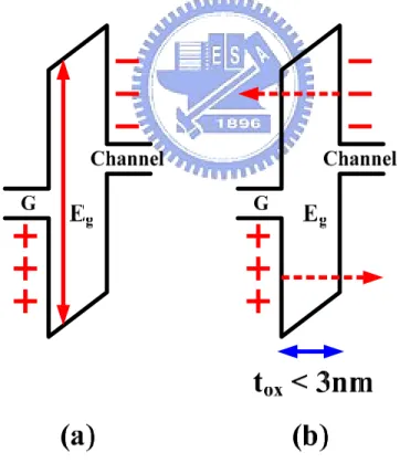
(29) Fig. 1.1. LSTP logic scaling-up of gate leakage current density limit and of simulated gate leakage due to direct tunneling. [ITRS 2003]. Fig. 1.2. Polysilicon depletion effects. 9.
(30) Chapter 2 Trends in Gate Oxide Scaling. 2.1. MOSFET Scaling Recall that a MOSFET ideally acts as a three-terminal switch, either connecting or. isolating the drain (D) and source (S) terminals based on the voltage applied to the controlling gate (G) terminal, as illustrated in Figure 2.1(a). In practice, this switching action is achieved through the use of a gate capacitor, as illustrated in Figure 2.1(b). Depending on the polarity of the voltage applied to the gate terminal, either positive or negative charge is induced in the channel region along the bottom plate of the gate capacitor. The channel charge either connects or isolates the drain and source nodes depending on the type of carrier contained in those regions.. The operation of the MOSFET depends critically on several properties of the gate dielectric material, SiO2. The wide insulating bandgap (Eg) of SiO2 electrically isolates charges in the gate and channel regions, so that the controlling gate terminal does not interfere with the flow of current in the channel region, as illustrated in Figure 2.2(a). Also, the interface between SiO2 and the underlying Si substrate is electrically of very high quality, allowing electric field lines originating at the gate electrode to penetrate into the channel region to accumulate or invert the surface charge. Prior to the development of the Si/SiO2 system, attempts to realize a field-effect transistor (FET) were hampered by the abundance of electrically active defects at the dielectric/semiconductor interface.. 10.
(31) The amount of charge (Q) induced in the channel region is given by the product of the gate oxide capacitance per unit area (Cox) and the voltage drop across the gate capacitor (V), Q = C oxV .. (2.1). Since Cox can be modeled as a parallel-plate capacitor, its value is given by. C ox =. k ox ε 0 , t ox. (2.2). where kox is the relative dielectric constant, ε0 is the permittivity of free space, and tox is the physical thickness of the dielectric material. Based on these relations, the drain-source current for a long-channel MOSFET operating in the saturation region can be expressed as. I ds =. 1 W µC ox (V gs − Vt ) 2 , L 2. (2.3). where µ is the channel mobility, W and L are the width and length of the channel region, respectively, Vgs is the gate-source potential, and Vt is the threshold voltage. Equations 2.2 and 2.3 reveal that reducing the lateral (L) and vertical (tox) dimensions of the device increases the current flow between the drain and source. Intuitively, this is because reducing tox increases Cox and hence the amount of channel charge, and reducing L decreases the distance the channel charge must travel to conduct a current. Reducing the gate oxide thickness (tox) along with the channel length (L) also helps to maintain the gate electrode’s control over short channel effects. Increased gate capacitance allows the gate potential to modulate more channel charge and is especially important as the supply voltage scales down. Much of the progress in Si microelectronics has been driven by the ability to continually shrink these and other critical dimensions of the MOSFET to increase performance and decrease die area, a process referred to as scaling [29]. 11.
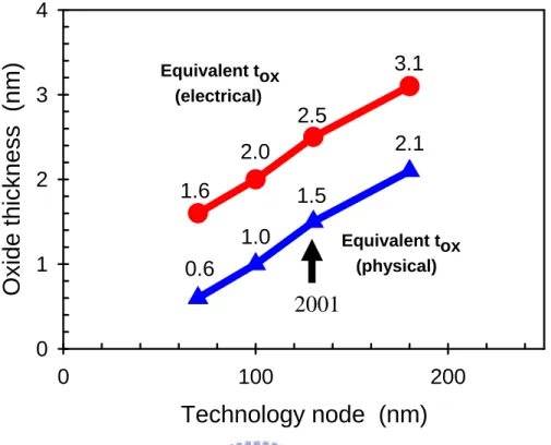
(32) 2.2. Recent Gate Oxide Scaling Trends The gate oxide has been aggressively scaled in recent generations. Figure 2.3 shows. extrapolated gate oxide scaling targets based on published data from recent Intel technologies [30]. The technology node refers to the smallest poly-Si gate length which can be defined by photolithography and roughly corresponds to the minimum channel length for a given process technology. A more complete list of projected transistor parameters is given in Table 2.1. The predictions are based on extrapolations of published state-of-the-art 180 nm technologies assuming channel length, supply voltage, and gate oxide thickness scaling factors of 0.7, 0.8, and 0.8, respectively [31]-[33]. These projections, representative of the current targets for high-performance logic technology, aggressively outpace those compiled in the 2000 update of the International Technology Roadmap for Semiconductors (ITRS). However, these data have been included and revised in the 2004 update of the ITRS, as shown in Table 2.2.. The two data sets in Figure 2.3 refer to the equivalent electrical and physical thickness of the gate oxide. The equivalent oxide thickness (EOT) refers to how thin a pure SiO2 layer would need to be in order to meet the gate capacitance requirements of a given technology. In a modern MOSFET device, the gate oxide behaves electrically as if it were 0.8−1.0 nm thicker than its physical thickness, because depletion in the poly-Si gate and quantization in the inversion layer each extend the centroids of charge modulated by the gate voltage by 0.4−0.5 nm [34].. 2.2.1. Gate Leakage and Static Power Dissipation. 12.
(33) A significant consequence of aggressively scaling the gate oxide is the resulting direct tunneling of carriers through the potential barrier presented by the insulator layer. As illustrated in Figure 2.2(b), when the thickness of the potential barrier becomes less than approximately 3.0 nm, substantial tunneling currents can flow through the gate oxide, leading to large static power dissipation. In addition, the gate and channel regions are no longer isolated from each other when tunneling occurs. Recent studies have shown that gate leakage can significantly impact circuit performance as a consequence, especially for analog and dynamic logic circuits.. Figure 2.4 shows extrapolated trends in power dissipation for high-performance CMOS logic based on published data from recent Intel technologies [30], [35]. Both active and static power components are shown. Traditionally, the main source of power dissipation in CMOS circuits has been active switching, which depends on the rate at which node capacitances are charged and discharged,. Pactive = NCV 2 f .. (2.4). N is the number of switching transistors, C is the total switched capacitance, V is the supply voltage, and f is the frequency of operation. The observed increase in active power with each generation reflects the trend towards higher levels of integration and higher frequency of operation, which more than offsets the reduction in device capacitance and supply voltage. Much more alarming is the rapid increase in static (i.e. standby) power dissipation beyond the 180 nm technology node. Static power is primarily due to subthreshold (Ioff) and gate (Igate) leakage currents. The extrapolation of the Igate component is based on quantum mechanical modeling of gate tunneling currents through ultrathin SiO2 layers by Lo et al. [34], [36]. As shown in Figure 2.4, standby power has been increasing much more rapidly than active power. 13.
(34) in recent generations, and if current trends continue, standby power will actually surpass active power beyond the 65 nm generation. Clearly, the exponential increase in the gate leakage, which arises from direct tunneling of carriers through the gate oxide, presents a serious limit to future CMOS scaling.. 2.2.2. Scaling Limit of SiO2. In addition to limitations arising from static power dissipation, there has recently been great interest in determining if a more fundamental limit to scaling SiO2 exists. One of the most convincing experiments which demonstrated that such a fundamental limit indeed exists is the work of Muller et al. from Bell Labs [37], [38]. Using a scanning transmission electron microscope (STEM) probe with 0.2 nm resolution, they studied the chemical composition and electronic structure of oxide layers as thin as 0.7−1.2 nm through detailed electron-energyloss spectroscopy (EELS) measurements. By moving the probe site-by-site through the ultrathin SiO2 layers, they mapped the local unoccupied density of electronic states, which provides insight into the local energy gap of the material, as a function of the probe position. In their work, the local energy gap was given by the separation between the highest occupied and lowest unoccupied states. They found that three to four monolayers of SiO2 were needed to ensure that at least one monolayer maintained a fully bulk-like bonding environment, giving rise to the wide, insulating bandgap of SiO2. Since the first and last monolayers form interfaces with Si and poly-Si respectively, they have bonding arrangements intermediate to those of bulk Si and bulk SiO2 and hence have energy gaps smaller than that of bulk SiO2. Based on these insights, Muller et al. concluded that the fundamental scaling limit of SiO2 is likely to be in the range of 0.7 to 1.2 nm. Another important insight from their study was that for a 1.0 nm oxide, a 0.1 nm increase in the root-mean-square (RMS) interface roughness can 14.
(35) lead to a factor of 10 increase in the gate leakage current, showing that the growth of such thin layers must be precisely controlled on atomic scales.. There has been remarkable agreement between experiment and theory regarding the scaling limit of SiO2. Theoretical studies by Tang et al. employing a Si/SiO2 interface model based on the β-cristobalite form of SiO2 showed that the band offset at the interface degraded substantially when the SiO2 layer was scaled to less than three monolayers [39]. The large reduction in the band offset was attributed to a reduction in the SiO2 bandgap and also suggested 0.7 nm as the scaling limit of SiO2. A more recent study by Kaneta et al. using a Si/SiO2 interface model based on β-quartz SiO2 directly computed the local energy gap as a function of position through the interface [40]. While the transition from bulk Si to bulk SiO2 in their model was structurally abrupt, it was found that the full bandgap of SiO2 was not obtained until the second monolayer of SiO2 was reached. Again, these calculations suggest that approximately 0.7 nm of SiO2 is the minimum required for substantial band offsets to develop at the interface, indicating the formation of a large bandgap.. Thus, both experiment and theory suggest that the bulk properties of SiO2, including the wide, insulating bandgap needed to isolate the gate and channel regions, cannot be obtained for films less than 0.7 nm thick. Since technology roadmaps predict the need for sub-0.6 nm gate oxides in future generations, it is unlikely that SiO2 will scale beyond the 70 nm generation, both from static power dissipation and fundamental materials science points of view.. 2.3. High-k Gate Dielectrics. 15.
(36) As an alternative to continuing to scale SiO2, recent effort has focused on the development of alternative high-k gate dielectrics. Recall that the traditional approach to scaling the gate dielectric has been to reduce tox to increase Cox,. C ox =. k ox ε 0 , t ox. (2.5). But now that gate leakage currents due to direct tunneling have reached unacceptably high levels, the more recent high-k approach is to increase the physical thickness of the film (thigh-k) to reduce the tunneling currents, yet at the same time obtain higher values of gate capacitance by using a dielectric material with a higher dielectric constant (khigh-k) relative to SiO2,. C high − k =. k high − k ε 0 t high − k. .. (2.6). Over the past several years, a wide variety of high-k dielectrics have been investigated as possible replacements for SiO2. Compared to just five or six years ago, a much shorter list of candidates is still being pursued today, due to the stringent requirements placed on the MOS dielectric material. In considering candidate gate dielectrics, it should be recalled that the dominance of the Si MOSFET over competing technologies has largely been attributed to the high quality of thermally grown SiO2 and the resulting Si/SiO2 interface. Other substrate materials provide higher intrinsic carrier mobilities or concentrations, yet none can match the electrical performance of the Si/SiO2 interface. Not surprisingly then, the most stringent requirements arise from the need to develop an alternative dielectric material whose Si interface properties match the high quality of the Si/SiO2 interface.. In the following sections, some of the important materials properties required of high-k 16.
(37) dielectrics are reviewed. Such considerations lead to the conclusion that only a few basic classes of materials are capable of meeting the requirements for a replacement dielectric material. Several excellent review papers discuss these and other material considerations for high-k dielectric applications in further detail [41]−[43]. A particularly important consideration is that the chosen high-k dielectric be scalable to future technology generations. Because of the immense costs associated with developing a replacement material for SiO2, which benefits from nearly 30 years of research, the industry requires a material which will not only meet the requirements for the upcoming 90 nm or 65 nm technologies, but can also be scaled to end-of-the-roadmap technology nodes.. 2.3.1. Target Dielectric Constant. To first order, a high-k film can be physically thicker than a pure SiO2 layer by the ratio of its dielectric constant to that of SiO2, and still provide the same gate capacitance, since. C ox =. k high − k ε 0 k ox ε 0 = C high − k = t ox t high − k. (2.7). and. ⎛ k high − k t high − k = ⎜⎜ ⎝ k ox. ⎞ ⎟⎟t ox , ⎠. (2.8). thus potentially reducing direct tunneling currents substantially. Equation (2.8) is often expressed in terms of the equivalent oxide thickness (EOT) described in Section 2.2. In the context of high-k dielectrics, EOT is defined as the thickness of a pure SiO2 layer which 17.
(38) provides the same gate capacitance as a high-k layer,. ⎛ k EOT = t ox = ⎜ ox ⎜k ⎝ high − k. ⎞ ⎟t high − k . ⎟ ⎠. (2.9). Recall from Figure 2.3 that the gate capacitance targets for the upcoming 90 nm and 65 nm technologies require dielectrics with physical EOT values of 1.0 nm and 0.6 nm, respectively. At first glance, it would seem that an arbitrarily high k-value would allow a substantially thick dielectric film to meet very small EOT targets. In practice, the extreme gate thickness-length aspect ratio that would result from a very high k-value and hence a very thick insulator leads to fringing field effects which undermine the gate electrode’s ability to maintain control of the channel. Device simulations have explored the impact of large k-values on threshold voltage roll-off and subthreshold swing to determine the upper range of desirable dielectric constants, which generally is believed to be on the order of 30 to 50 [44]. The lower range of acceptable dielectric constants depends on the EOT requirements of a given technology generation. It is generally believed that pure or nitrided SiO2 with dielectric constants close to 4 will provide physical EOTs down to about 1.6 nm; near-term alternatives such as Si3N4 or oxynitride stacks with nitrided SiO2 interfaces with k-values near 7 will provide physical EOTs down to about 1.1 nm; and pure metal oxides or pseudo-binary alloys of metal oxides with dielectric constants in the range of 15 to 25, providing a factor of four to six improvement over SiO2, will provide physical EOTs down to about 0.6 nm.. It should be noted that some of the near-term materials such as Si3N4 and the metal oxide Al2O3 are attractive from the point of view of integration, since substantial experience and equipment infrastructure for processing both materials exist. Due to the relatively low gains in the dielectric constant relative to SiO2, however, these materials are likely to be intermediate solutions at best. It is also worth mentioning that the ferroelectric class of materials which has 18.
(39) been pursued for 1 Gb and beyond dynamic random access memory (DRAM) storage capacitors provide k-values in the range of 100 to 1000, far in excess of the requirements for a gate dielectric [41]. In addition, ferroelectric materials generally require a complex composite structure to promote stability and adhesion to adjoining layers, so that using them as transistor gate dielectrics is not feasible. Hence, substantial new investments in materials research and technology development are needed, above and beyond the existing efforts in the DRAM community, to realize alternative gate dielectrics for logic technologies.. Many high-k materials consist of oxides and alloys of d-electron transition metals. Representative transition metal oxides include: column 3B materials such Y2O3 and La2O3; column 4B materials such as ZrO2 and HfO2; and column 5B materials such as Ta2O5. It is well-known that the static (i.e. low frequency) dielectric constants of such metal oxides have significant electronic and ionic contributions at the frequencies of interest [45]. The electronic contribution arises from the polarization of electrons in response to an applied electric field, whereas the ionic contribution depends on the displacement of the ions themselves in response to an electric field. To first order, the additional shells of electrons in a heavy transition metal compared to a lighter atom allow for greater electronic polarization for a given electric field strength. It has also been observed that the d-electron metal transfers nearly all of its valence electrons to the oxygen atom, resulting in increased ionicity and hence polarization. In addition, the bonding between many d-electron transition metals and oxygen exhibit a softening of the phonon mode. In other words, the natural vibration frequency associated with the metal-oxygen bond is lowered. This allows the relatively low frequency excitation common in microelectronics applications to couple into the vibrational mode, leading to large displacements of the metal atom. The ability to model both the electronic and ionic components of the dielectric response is thus important for investigation of high-k materials. 19.
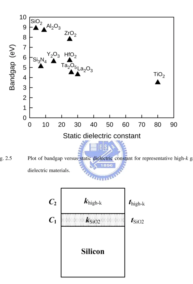
(40) In addition to pure transition metal oxides, there is also considerable interest in pseudo-binary alloys for high-k applications. Representative examples include the silicate system, such as ZrSixOy, which can be thought of as an alloy between the pure metal oxide ZrO2 and SiO2, (ZrO2)x(SiO2)1-x; and the aluminate system, such as LaAlxOy, which is an alloy between La2O3 and Al2O3, (La2O3)x(Al2O3)1-x. The motivation for the use of these alloys over pure metal oxides arises from their interface properties with Si, as described in Section 2.4.. 2.3.2. Bandgap and Band Offsets. Since an important function of the gate dielectric is to isolate the gate terminal from the current-carrying channel region, it needs to be a good insulator. SiO2 provides a wide bandgap on the order of 9 eV, substantially larger than the 1 eV bandgap of Si. A closely related property is the height of the potential barrier presented to tunneling electrons from the conduction band and to tunneling holes from the valence band. At the Si/SiO2 interface, these band offset energies are relatively symmetric, so that barriers on the order of 4 eV are presented to both electrons and holes. Any degradation of the bandgap results in lower band offset energies which compromise the potential tunneling reduction obtained by using a material with a higher dielectric constant and hence a physically thicker film.. It has been observed that most high-k materials have smaller bandgaps relative to SiO2. Figure 2.5 illustrates the approximately inverse relation between bandgap and static dielectric constant obeyed by a number of representative high-k dielectrics. This behavior is expected qualitatively since stronger polarizability implies weaker bonding, and weaker bonding implies a smaller separation between bonding and antibonding energies [46]. The implied 20.
(41) tradeoff between dielectric constant and bandgap severely limits the applicability of candidate materials at the upper range of target dielectric constants. For example, early high-k efforts focused on Ta2O5 and TiO2, since they provided large dielectric constants and substantial processing experience with the materials existed from DRAM applications [47]−[50]. However, their bandgaps are substantially smaller than that of SiO2, with estimated values of 4.5 eV and 3.5 eV for Ta2O5 and TiO2, respectively [42]. Interestingly, Al2O3 presents an exception to this general trend and provides approximately twice the k-value of SiO2 while maintaining a large bandgap.. 2.3.3. Si Interface Properties. The feasibility of any high-k dielectric ultimately depends on the quality of its interface with Si. Two particularly important interface considerations are thermal stability and defect formation. Many of the early metal oxides such as Ta2O5 and TiO2 which were pursued because of their previous use in DRAM processes have been found to be thermally unstable in direct contact with Si [48], [50], [51]. For both materials, reactions have been observed in which thick interfacial layers form between the metal oxide and the Si substrate. Specifically, Alers et al. observed the formation of a 2.0 nm thick interfacial region after Chemical Vapor Deposition (CVD) of Ta2O5 on HF-last-Si at 400°C [48]. Similar observations of interfacial reaction have been made for TiO2 films deposited directly on HF-last-Si [50]. Since the channel transport properties were determined by nominally Si/SiO2-like interfaces for both materials, reasonable channel mobilities were obtained. The Si/SiO2 interface is known to have a very low density of interface states arising from unsaturated surface bonds and other electrically active imperfections. Interface states lead to degradation of on-current, since carrier mobility is limited by scattering at the interface due to the strong vertical electric fields 21.
(42) present in the channel. In the case of the TiO2 device, deliberate efforts to suppress the growth of the interfacial layer led to substantial charging and degradation of peak channel mobility from 150 cm2/V-sec to 60 cm2/V-sec.. For both Ta2O5 and TiO2, the formation of an interfacial oxide layer appears inevitable and necessary to maintain good transport properties at the Si interface. In fact, interfacial reaction is expected for these materials based on analysis of equilibrium phase diagrams [42]. While it is difficult to directly determine the chemical composition of such thin layers, it is generally believed that a SiO2-like layer with a relatively low dielectric constant forms, as illustrated by Figure 2.6. The formation of an interfacial low-k layer between the Si substrate and the high-k film is highly undesirable, since then the gate dielectric appears electrically as a series capacitance whose effective capacitance is less than that of the high-k layer alone,. 1 1 1 = + . C eq C1 C 2. (2.10). Assuming that the interfacial layer has the dielectric properties of SiO2, Equation (2.10) can be re-written in terms of the following relation for the EOT of the dielectric stack.. ⎛ k SiO2 t eq = t SiO2 + ⎜ ⎜k ⎝ high − k. ⎞ ⎟t high − k ⎟ ⎠. (2.11). For a given EOT (teq) target, any non-zero tSiO2 reduces the thickness of the high-k film which can be used, thus increasing the tunneling transmission through the stack. Furthermore, the minimum EOT can never be less than tSiO2, so that the interfacial oxide layer limits the maximum achievable capacitance of the gate stack.. 22.
(43) 2.4. Zirconium and Hafnium Silicates Zirconium (Zr) and hafnium (Hf) silicates are promising high-k dielectrics developed. largely to overcome the interface stability issues suffered by many high-k binary metal oxides [52]−[54]. Ternary phase diagrams of the Zr-Si-O system reveal that the binary metal oxide ZrO2 as well as the compound silicate ZrSiO4 should be thermodynamically stable in direct contact with Si. Since Zr and Hf are isoelectronic elements, it is expected that HfO2 and HfSiO4 should also be stable on Si.. In practice, interface reactions, much like those described in the previous section for other metal oxides, have been observed for nearly all ZrO2 and HfO2 films deposited directly on Si [50], [55], [56]. High resolution transmission electron microscope (HRTEM) measurements by Campbell et al. revealed that interfacial layers of 0.9 nm and 1.2 nm thickness were formed when depositing ZrO2 and HfO2 directly on Si, respectively [50]. Medium energy ion spectroscopy (MEIS) and x-ray photoelectron spectroscopy (XPS) analysis showed that the interfacial layer was SiO2-like, not a silicate. In contrast, Lee et al. found that ZrO2 and HfO2 films deposited directly on Si using a magnetron sputtering technique gave rise to a silicate interfacial layer [55]. Copel et al. also found that ZrO2 deposition by atomic layer chemical vapor deposition (ALCVD) on HF-last-Si led to discontinuous nucleation with islands of ZrO2 interspersed along the Si interface [56]. Atomic force microscopy also revealed a large RMS roughness of 0.57 nm along the interface.. The variability in the interfacial layer following ZrO2 and HfO2 deposition leads to the conclusion that the growth of such layers is difficult to control. Instead, recent efforts toward integrating ZrO2 and HfO2 films have focused on first growing a high quality, well controlled, ultrathin SiO2 layer prior to ZrO2 deposition. Perkins et al. deposited ALCVD ZrO2 films on chemically grown oxides and obtained EOT < 1.4 nm [57]. Having an underlying SiO2 layer 23.
(44) also leads to the desirable electrical properties of a Si/SiO2 interface which helps to maintain high channel carrier mobility. Of course, the minimum EOT is still limited by the extent of the interfacial SiO2 layer as described previously.. Another potential problem with ZrO2 and HfO2 is that they have been observed to crystallize at relatively low temperatures. Polycrystalline films may exhibit high leakage paths along grain boundaries which act as trapping centers. Thus, in general, amorphous dielectrics which resist recrystallization up to relatively high temperature are desirable for gate dielectric applications.. To overcome the challenges of pure ZrO2 and HfO2 films, Wilk and Wallace proposed the use of Zr and Hf silicates as promising high-k gate dielectrics [42], [52]−[54]. By alloying two different oxides, such as ZrO2 and SiO2 in the case of Zr silicate, (ZrO2)x(SiO2)1-x, they believed that it may be possible to retain the desirable properties of both oxides while eliminating the undesirable properties of each. By explicitly incorporating SiO2 during deposition of ZrO2 precursors, the driving force for reaction between the dielectric and the Si substrate is reduced, so that the interface is more likely to behave like the desirable Si/SiO2 interface. This allows better control of the Si interface properties. It is generally believed that silicate deposition results in a single, uniform high-k layer in direct contact with Si. Combining a poly-crystalline film like ZrO2 with an amorphous one like SiO2 also leads to an amorphous silicate phase.. At the same time, by incorporating some amount of ZrO2 into the SiO2 film, the enhanced polarizability of Zr-O bonds relative to Si-O bonds leads on average to a higher dielectric constant for material. While many different silicate systems are possible, column IVB elements such as Zr and Hf are expected to substitute well for Si atoms, thus reducing the possibility of forming dangling (i.e. unsaturated) bonds at the Si interface. The notion of 24.
(45) doping SiO2 with Zr or Hf also leads to a natural scaling scenario for the silicate system. By progressively increasing the Zr or Hf concentration, the k-value can be steadily increased, up to a limit, to meet the gate capacitance requirements for future technology generations.. The increased control over interface properties comes at the expense of a lower dielectric constant relative to pure ZrO2 or HfO2. Depending on the metal concentration, the dielectric constant is believed to scale between 4, corresponding to pure SiO2, and approximately 15 to 20 for stoichiometric ZrSiO4 or HfSiO4, since pure ZrO2 and HfO2 are thought to have dielectric constants close to 25 and 35, respectively [54]. Si-rich compositions are preferred to maintain thermal stability with the Si substrate. Preliminary theoretical work by Jun et al. suggests that both ZrSiO4 and HfSiO4 have dielectric constants near 12, toward the lower end of the above range.. The lower dielectric constant of the silicates relative to the pure metal oxides does not necessarily imply a smaller gate capacitance. To illustrate this point, Figure 2.7 shows two possible gate stack structures. Figure 2.7(a) depicts a pure metal oxide (e.g. ZrO2 with k = 25) which requires a 0.5 nm interfacial SiO2 layer with k = 4. Figure 2.7(b) shows a silicate layer (e.g. Zr silicate with k = 16) which forms a single, uniform high-k layer in direct contact with Si. Using Equations (2.9) and (2.11), it is straightforward to show that both gate stack structures achieve the same equivalent gate capacitance, corresponding to EOT values of 1.0 nm. Surprisingly, the lower-k silicate layer can be physically thicker than the higher-k ZrO2 layer, so that less tunneling is expected for the silicate stack. This is due to the fact that the silicate is believed to form a single, uniform high-k layer, thus avoiding the formation of a low-k interfacial region.. 25.
(46) 2.5. Summary This chapter has reviewed recent trends in gate oxide scaling. The aggressive scaling. requirements for upcoming technologies suggest that SiO2 cannot be scaled beyond the 65 nm generation. The desirable properties of alternative high-k dielectric materials have also been described. An important consideration is that the chosen dielectric material be scalable to future technology nodes. Of the various requirements, it is likely that achieving a high quality interface with the underlying Si substrate will be the most stringent. This requirement has motivated the development of the silicate system, which is believed to form a high quality Si/SiO2-like interface while eliminating the need for an explicit interfacial oxide layer, which limits the achievable EOT values of gate stacks employing pure metal oxides.. 26.
(47) Table 2.1. Projected transistor parameters for future technology generations.. Generation (nm). 180. 130. 100. 70. Scaling factor. Lgate (nm). 100. 70. 50. 35. 0.7x. Vdd (V). 1.5. 1.2. 1.0. 0.8. 0.8x. 3.1. 2.5. 2. 1.6. 0.8x. 2.1. 15. 1.0. 0.6. 0.8x. 20. 40. 80. 160. 2x. Tox, electrical (nm) Tox, physical (nm) Ioff at 25°C (nA/µm). Table 2.2. Selected excerpts from the 2004 update of the International Technology Roadmap for Semiconductors.. Year. 2001. Technology Node 130nm. 2004. 2007. 2010. 2013. 2016. 90nm. 65nm. 45nm. 32nm. 22nm. Lgate (nm). 65. 37. 25. 18. 13. 9. Vdd (V). 1.2. 1.2. 1.1. 1. 0.9. 0.8. Tox,physical (nm). 1.5. 1.2. 0.9. 0.7. 0.6. 0.5. Gate leakage at 100°C (µA/µm). 0.01. 0.17. 0.23. 0.33. 1. 1.67. Solutions unknown. 27.
(48) Fig. 2.1. (a) The MOSFET ideally acts as a 3-terminal switch. (b) Practical realization of the MOSFET requires a gate capacitor.. Fig. 2.2. (a) Simplified band diagram of the MOS system. (b) Direct tunneling of carriers through the insulator potential barrier can occur for thin dielectric layers.. 28.
(49) Oxide thickness (nm). 4 3.1. Equivalent tox (electrical). 3. 2.5 2.1. 2.0 2. 1.6. 1.5 1.0. 1. Equivalent tox (physical). 0.6. 2001 0 0. 100. 200. Technology node (nm) Fig. 2.3. Extrapolated gate oxide scaling trend for recent CMOS technologies.. Fig. 2.4. Extrapolated trend of active and leakage power dissipation for state-of-the-art CMOS technologies. 29.
數據
+7
Outline
Challenge of Gate Dielectric Scaling
Scope and Organization of the thesis
Recent Gate Oxide Scaling Trends
Zirconium and Hafnium Silicates
Conclusions
Enhanced Negative Bias Temperature Instability
Constant Current Stress and Charge-to-Breakdown
Leakage Mechanism of the MIM Capacitors
Suggestions for Future Work
相關文件
Valor acrescentado bruto : Receitas do jogo e dos serviços relacionados menos compras de bens e serviços para venda, menos comissões pagas menos despesas de ofertas a clientes
The prepared nanostructured titania were applied for the photoanodes of dye-sensitized solar cell.. The photoanodes were prepared by the doctor blade technique and the area
◦ 金屬介電層 (inter-metal dielectric, IMD) 是介於兩 個金屬層中間,就像兩個導電的金屬或是兩條鄰 近的金屬線之間的絕緣薄膜,並以階梯覆蓋 (step
It’s not chocolate that causes problems, but the highly processed nature of the products containing chocolate and high levels of sugar and fat.. While it’s great that chocolate
• When the coherence bandwidth is low, but we need to use high data rate (high signal bandwidth). • Channel is unknown
• When the coherence bandwidth is low, but we need to use high data rate (high signal bandwidth). • Channel is unknown
To reduce the leakage current related higher power consumption in highly integrated circuit and overcome the physical thickness limitation of silicon dioxide, the conventional SiO
To reduce the leakage current related higher power consumption in highly integrated circuit and overcome the physical thickness limitation of silicon dioxide, the conventional SiO 2
