損耗基板模型建立與高頻雜訊模擬射頻場效電晶體與探針墊結構之研究
94
0
0
全文
(2) 損耗基板模型建立與高頻雜訊模擬 射頻場效電晶體與探針墊架構之研究 The Lossy Substrate Model for RF MOSFET High Frequency Noise Simulation under Various Pad Structures 研究生:蔡依修. Student : Yi-Hsiu Tsai. 指導教授:郭治群 博士. Advisor : Dr. Jyh-Chyurn Guo. 國 立 交 通 大 學 電子工程學系 電子研究所 碩 士 論 文. A Thesis Submitted to Department of Electronics Engineering & Institute of Electronics College of Electrical and Computer Engineering National Chiao Tung University in partial Fulfillment of the Requirements for the Degree of Master In Electronics Engineering August 2007 Hsinchu, Taiwan, Republic of China. 中華民國九十六年八月.
(3) 損耗基板模型建立與高頻雜訊模擬 射頻場效電晶體與探針墊結構之研究 研究生:蔡依修. 指導教授:郭治群 博士. 國立交通大學 電子工程學系 電子研究所. 摘要 在本論文中,首先對金氧半場效電晶體的雜訊理論與原理、各種不同雜訊模型的 介紹與雜訊量測的原理及架構做基本的介紹其中包括熱雜訊(高頻)與閃爍雜訊(低 頻)。接下來進入本論文的核心部分,利用 130nm 製程研製之射頻互補式金氧半場效 電晶體來建立並驗證一個寬頻且可調性的矽基板損耗模型。在第三章,利用開路探針 墊的量測結果建立一個可以適用於包括:損耗(lossy)、標準(normal)、小型(small)等 三種不同探針墊架構的改良型損耗矽基板模型。在第四章,藉由量測電晶體的電流電壓特性、轉導與導納參數來校正電晶體的本質特性模型,其中包跨電流-電壓、電容 -電壓模型。在第五章,探討不同的探針墊架構其矽基板損耗效應所貢獻的額外雜訊的 影響。藉由將探針墊的等效電路搭配經過準確校正的本質元件模型構成的完整電路來 進一步驗證改良型矽基板損耗模型。已完成的可調性矽基板模型可以準確的預測損耗 型探針墊 (lossy pad)在雜訊參數上所表現的異常閘極指叉數(gate finger number)相關 性與對頻率的非線性關係。更進一步的,可以有效分析探針墊架構,如金屬堆疉層次 與形狀大小,以及連線佈局之影響,得以準確模擬矽基板損耗經由傳輸線與探針墊所 貢獻的額外雜訊。最後,改良型損耗矽基板模型提供了一個適當且能有效降低由傳輸 線與探針墊所貢獻的額外雜訊的佈局方法。本論文中,小型(small) 探針墊可以很明顯 的降低由探針墊所貢獻的外在雜訊,使直接量測到的雜訊特性幾乎接近元件的本質雜 訊特性。. i.
(4) A Lossy Substrate Model for RF MOSFET High Frequency Noise Simulation under Various Pad Structures Student : Yi-Hsiu Tsai. Advisor : Dr. Jyh-Chyurn Guo. Department of Electronics Engineering and Institute of Electronics National Chiao Tung University. ABSTRACT In this thesis, the basic noise theory, noise models, noise measurement principles and the equipment configuration will be introduced at the first place. Both thermal noises at high frequency and flicker noise dominant at low frequency will be covered. Then a broadband and scalable lossy substrate model is developed and validated for nanoscale RF MOSFET, which were fabricated by 130nm 1.2V CMOS technology. In chapter 3, an enhanced lossy substrate model adopting various pad structures, such as lossy, normal, and small pads was developed based on open pad S-parameters at high frequency up to 40 GHz. In chapter 4, the intrinsic MOSFET model through extensive calibration on I-V and C-V models will be presented. The model calibration was done based on the measured I-V, transconductance, and admittance from Y-parameters. In chapter 5, a detailed discussion on the pad structures effect on RF noise will be provided. The enhanced lossy substrate model is verified by integration with the intrinsic devices model for full circuit model. The scalable lossy substrate model can consistently predict the abnormally strong finger number dependence and nonlinear frequency dependence of noise figure (NFmin) revealed by the devices with lossy pads. Furthermore, the scalable model can precisely distribute the substrate loss between the transmission line (TML) and pad with various metal topologies and the resulted excess noises. Finally, the enhanced model provides useful guideline for appropriate layout of pads and TML to effectively reduce the excess noises. The remarkably suppressed noise figure to ideally intrinsic performance can be approached by the small pad in this thesis. ii.
(5) 誌謝. 時間過的很快,兩年的碩士班生涯過去了,雖然我加入高頻奈米元件實驗室的時 間不過一年多,不過這一年來,不管是研究上或是做人處世上所學到的都很多,也進 步很多,首先我要感謝我的指導老師 郭治群教授,在研究方法與態度上的指導與鞭 策,以及不斷的替實驗室尋求研究資源與實驗設備,讓我們能有最好的研究環境,並 且時常給予學生專業知識上的傳授與建議,是我的研究能有成果最重要的關鍵之一; 也感謝老師不斷的鼓勵我繼續深造,並提供良好之進修機會,讓我可以無後顧之憂的 繼續攻讀博士學位。此外特別要感謝林益民學長在我剛進來實驗室的時候,不遺餘力 的悉心指導,讓我能再最短的時間內踏入這個陌生的領域。另外要感謝 NDL 的研究 員 黃國威博士 在研究設備上的支持,讓我能夠學習到高頻量測,也感謝 RFTC 的工 程師們,邱佳松、王生圳等學長在量測過程上的建議與指導,讓我在量測的過程中受 益匪淺。也感謝在高頻奈米實驗室的成員們,仁嘉、冠旭、國良,因為你們的陪伴, 在做研究的過程中,不至於太苦悶。當然還要感謝陪伴我兩年的室友,書維、政鴻、 祥倫、承德,謝謝你們這兩年來的照顧以及陪伴我度過無數次的狂歡與低潮。最後要 感謝默默在背後支持我的家人,感謝你們的養育之恩與教導我做人處世的道理,使我 能有積極上進的求學態度,讓我可以順利的完成碩士學位。. iii.
(6) Contents. Chinese Abstract ……………………………………………………………...…………i English Abstract……………………………………………..……………………….….ii Acknowledgement………………………………………………………………….......iii Contents…………………………………………………………………………….…......iv Figure Captions……..……………………………….………………………….………vi Table Captions…………..……………….…………………………..…………….........ix Chapter 1 Introduction 1.1 Motivation…………………………………………………………………...1 1.2 Overview…………………………………………………………………….2. Chapter 2 Noise Theory and Noise Measurement Technique 2.1 Noise Source………………………………………………………….……..4 2.1.1 Flicker Noise…………………………………………..………...……..5 2.1.2 Thermal Noise…………………………………………..………...……6 2.1.3 Thermal Noise in MOSFETs…………………………..….............……7 2.2 Two-Port Noise Theory…………………………...…………………….....10 2.2.1 Noise Figure……………………………………..…………………....10 2.2.2 Noise Parameters…...………………………...……...…………....…..11 2.3 Thermal Noise Model……………………………………..……….……...13 2.4 Flicker Noise Model……………………………………….…...……….…16 2.5 High Frequency Noise Measurement…………………….…...………….20 2.5.1 System Configuration…………………………...……….……….…..21 2.5.2 System Calibration and Measurement………………....……….…….22. Chapter 3 Scalable Lossy Substrate Model for Various Pad Structures iv.
(7) 3.1 GSG Pad Layout Structures…………..……………………..……………27 3.2 Lossy Substrate Model Development For Various Pad Structures.........28. Chapter 4 RF MOSFET Intrinsic I-V and C-V Model Calibration 4.1 I-V and C-V Modeling Theory Valid for Sub-100nm MOSEFT……….38 4.2 DC I-V Model Development……………….……………………………...39 4.3 Intrinsic C-V Model Development…………………..…...……............…41. Chapter 5 Lossy Substrate Model to Predict Pad Structure Effect on RF Noise-Broadband Accuracy & Scalability 5.1 Equivalent Circuit Model Verification…………….....…………………..51 5.2 Pad Structures Effect On RF Noise ……………...…………..…......……55. Chapter 6 Conclusion 6.1 Summary……………………………………………………….………......73 6.2 Future Work…………………………………………………………….…73 6.2.1 Low Noise Measurement and Modeling………..……….…….……...73 6.2.2 Ultra Low Power Design………………………………...…………...74. Bibliography………………………………………………………………………….....75 Appendix A The Y-Factor Method and Noise Figure Correction…….........78 Appendix B Modified Open-Short De-embedding……………………….…....80 Vita…………………………………………………………………………………….…..83. v.
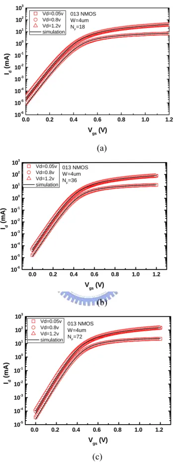
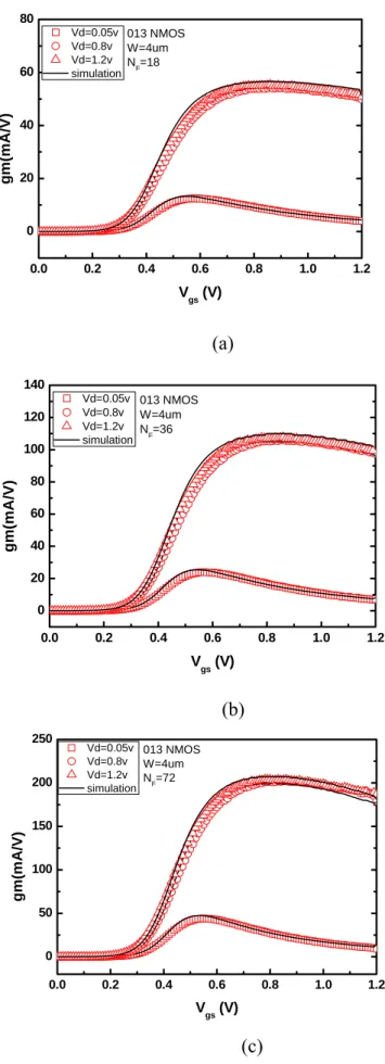
(8) Figure Captions Chapter 2 page Fig. 2.1. (a)Equivalent network for computing thermal noise of a resistor…….......... 25. Fig. 2.1. (b)(c)Thermal noise model for a resistor………………………………….... 25. Fig. 2.2. Schematic diagram of a MOSFET operated in saturation condition….......... 25. Fig. 2.3. Schematic for BSIM4 channel thermal noise modeling (a) tnoiMod=0 (b) tnoiMod=1…………………………………………………………………. Block diagram of ATN NP5B noise figure measurement system configuration…………………………………………………………………. Fig. 2.4. 26 26. Chapter 3 Fig. 3.1. Fig. 3.2 Fig. 3.3 Fig. 3.4 Fig. 3.5. Fig. 3.6. 3D schematics of GSG pads (a) lossy pad scheme:S-pads of stacked metals from M2 to M8 (b) normal pad:S pads of top metal (M8) only…………………………………………………………….…………… The equivalent circuit schematics of enhanced lossy substrate open pad model……………………………………………………………………….. (a) Equivalent circuit model derivation by circuit analysis………………... (b) Pad model parameter extraction flow…………………………………... Pad model parameters scalability for various pad structure……………….. Comparison of open pad S-parameters between measurement and lossy substrate model for three pad schemes, lossy, normal, and small (a) mag(S11) (b) phase(S11) (c) mag(S22) (d) phase(S22)……………………….. Comparison of open pad Y-parameters for three pad structures (a) re(Y11) (b) imag(Y11) (c) re(Y22) (d) imag(Y22)…………………………………….. 31 32 33 34 36. 36 37. Chapter 4 Fig. 4.1 Fig. 4.2 Fig. 4.3 Fig. 4.4. Modeling results of DC Id-Vd for Vg=0~1.2V with 0.2 Vg step. (a)NF=18 (b)NF=36 (c)NF=72………………………………………………………… Modeling results of DC Id-Vg for Vd=0.05, 0.8, 1.2V (a)NF=18 (b)NF=36 (c)NF=72……………………………………………………………………. Modeling results of DC log scale Id-Vg for Vd=0.05, 0.8, 1.2V (a)NF=18 (b)NF=36 (c)NF=72………………………………………………………… Modeling results of gm-Vg for Vd=0.05, 0.8, 1.2V (a)NF=18 (b)NF=36 (c)NF=72……………………………………………………………………. vi. 45 46 47 48.
(9) Fig. 4.5. Category diagram of gate capacitances in MOSFETs..……………………. 49. Fig. 4.6. Gate capacitances modeling results under various Vg (a)NF=18, (b) NF=36, (c)NF=72………………………………………………………….... 50. Chapter 5 Fig. 5.1. MOSFET device modeling flow…………………………............................ 59. Fig. 5.2. Full circuit model includes intrinsic MOSFET device and pad model…......................................................................................................... Intrinsic MOSFET modeling results with good match in terms of (a)gm, (b)fT (c)Cgg, (d)Cgd, and over wide range of biases or currents………………….............................................................................. Comparison of measured and simulated S11 by full circuit model for 100nm NMOS (NF=18,36,72) adopting 3 different pads, (a)lossy pad (b)normal pad (c)small pad (d)intrinsic S11 by pad de-embedding…….….. Comparison of measured and simulated S22 by full circuit model for 100nm NMOS (NF=18,36,72) adopting 3 different pads, (a)lossy pad. 60. (b)normal pad (c)small pad (d)intrinsic S22 by pad de-embedding……....... Comparison of measured and simulated S21 by full circuit model for 100nm NMOS (NF=18,36,72) adopting 3 different pads, (a)lossy pad (b)normal pad (c)small pad (d)intrinsic S21 by pad de-embedding………... Comparison of measured and simulated S12 by full circuit model for 100nm NMOS (NF=18,36,72) adopting 3 different pads, (a)lossy pad (b)normal pad (c)small pad (d)intrinsic S12 by pad de-embedding............... Comparison of measured and simulated Y11 by full circuit model for 100nm NMOS (NF=18, 36, 72) adopting 3 different pads, (a)lossy pad (b)normal pad (c)small pad (d)intrinsic Y11 by pad de-embedding……….. .Comparison of measured and simulated Y12 by full circuit model for 100nm NMOS (NF=18,36,72) adopting 3 different pads, (a)lossy pad (b)normal pad (c)small pad (d)intrinsic Y12 by pad de-embedding……….. Comparison of measured and simulated Y21 by full circuit model for 100nm NMOS (NF=18,36,72) adopting 3 different pads, (a)lossy pad (b)normal pad (c)small pad (d)intrinsic Y21 by pad de-embedding….......... Comparison of measured and simulated Y22 by full circuit model for 100nm NMOS (NF=18,36,72) adopting 3 different pads, (a)lossy pad (b)normal pad (c)small pad (d)intrinsic Y22 by pad de-embedding……….. Comparison of measured and simulated NFmin by full circuit model for 100nm NMOS (NF=18, 36, 72) adopting 3 different pads, (a) lossy pad (b) normal pad (c)small pad (d)intrinsic NFmin by lossy substrate de-embedding………………………………………………………………. 62. Fig. 5.3. Fig. 5.4. Fig. 5.5. Fig. 5.6. Fig. 5.7. Fig. 5.8. Fig. 5.9. Fig.5.10. Fig.5.11. Fig.5.12. vii. 60. 61. 63. 64. 65. 66. 67. 68. 69.
(10) Fig.5.13. Fig.5.14. Fig.5.15. Fig.5.16. Fig.5.17. Fig.5.18. Comparison of measured and simulated Rn by full circuit model for 100nm NMOS (NF=18,36,72) adopting 3 different pads, (a)lossy pad (b)normal pad (c)small pad (d)intrinsic Rn by lossy substrate de-embedding................................................................................................ Comparison of measured and simulated Re(Yopt) by full circuit model for 100nm NMOS(NF=18,36,72) adopting 3 different pads,(a)lossy pad (b)normal pad (c)small pad (d)intrinsic Re(Yopt) by lossy substrate de-embedding……………………………………………………………… Comparison of measured and simulated Im(Yopt) by full circuit model for 100nm NMOS (NF=18,36,72) adopting 3 different pads, (a)lossy pad (b)normal pad (c)small pad (d)intrinsic Im(Yopt) by lossy substrate de-embedding……………………………………………………………… Measured and simulated four noise parameters for 100nm NMOS by full circuit model of lossy,normal,small pads and comparison with intrinsic ones after lossy substrate de-embedding,NF=18 (a) NFmin, (b)Rn, (c)Re(Yopt), (d)Im(Yopt)................................................................................. Measured and simulated four noise parameters for 100nm NMOS by full circuit model of lossy,normal,small pads and comparison with intrinsic ones after lossy substrate de-embedding,NF=36 (a) NFmin, (b)Rn, (c)Re(Yopt), (d)Im(Yopt) …………………………………………………… Measured and simulated four noise parameters for 100nm NMOS by full circuit model of lossy,normal,small pads and comparison with intrinsic ones after lossy substrate de-embedding,NF=72(a) NFmin, (b)Rn, (c)Re(Yopt), (d)Im(Yopt)…………………...……….….................................. 69. 70. 70. 71. 71. 72. Appendix B Fig. B.1. Equivalent circuit of test structure with DUT…………………………….... 81. Fig. B.2. Equivalent circuit of open pad…………………………………………….... 82. Fig. B.3. Equivalent circuit of short pad……………………………………………... 82. viii.
(11) Table Captions Chapter 3 Table 3.1. Pad model parameters for various pad structures………………………. 35. Model parameters for gate capacitances modeling…………………….. 44. (a)Intrinsic MOSFET model parameters for various NF……………………............... (b)Pad model parameters for various pad structures………………….......... 54. Chapter 4 Table 4.1. Chapter 5 Table 5.1. ix.
(12) Chapter 1 Introduction The aggressive CMOS device scaling to sub-100-nm regime has driven dramatic reduction of gate delay to approach 10 ps (1p=10-12) and the remarkable increase of the unit current gain cut-off frequency to well beyond 100 GHz. Compact MOSFET model with broadband accuracy and scalability is recognized as a critical engine to facilitate the success of RF CMOS circuit design. The increasing demand on low power and low noise for wireless communication escalates the importance of noise characterization and. modeling. However,. the complicated noise coupling through the lossy pads, lossy substrate, and transmission lines (TML) will contribute excess noises and make the high frequency noise measurement and simulation a dramatic challenge.. 1.1 Motivation It is a difficult task to extract RF CMOS noise accurately while its scalability with device scaling is quite important for low noise RF circuit design. The challenges arise from the strong dependence of RF noise on the parasitic and coupling effect associated with the gate, lossy substrate, TML, and lossy pads. Regarding the lossy pad rendered through pad-to-substrate coupling, the impact is increasing for miniaturized devices and particularly worse for sub-100-nm Si RF CMOS. The extrinsic minimum noise figure (NFmin) before de-embedding may be dominated by the lossy substrate , TML, and lossy pad effect. However, a reliable noise de-embedding method to assure accurate extraction of intrinsic noise remains a difficult subject and is particularly challenging for nanoscale devices. A noise correlation matrix method [1] was proposed to deembed these effects but the complicated matrices calculation sometimes suffers fluctuation at very low noise level and poor accuracy in frequency dependence [2-3]. In our previous work, a lossy substrate model was developed to 1.
(13) predict the measured noise and a lossy substrate de-embedding method can be easily performed through circuit simulation for precise extraction of intrinsic noise [4-6]. The accuracy has been proven by sub-100 nm NMOS with various finger numbers and operation under varying frequencies and biases. Furthermore, a scalable lossy substrate model is desirable to enable prediction for on-chip devices. This demand triggers our motivation of this study on the excess noise coupling from lossy substrate, (TML and pads with various metal topologies. The enhanced lossy substrate model and lossy substrate de-embedding method have been extensively verified and justified by nanoscale devices adopting various pad structures.. 1.2 Overview A broadband and scalable lossy substrate model has been developed and validated for nanoscale RF MOSFETs with different finger numbers and adopting various pad structures such as lossy, normal and small pads. Chapter 2 gives an introduction to the classification and physical mechanism of noises in MOSFETs. The noise measurement theory and measurement system configuration are also covered. In chapter 3, we purpose an enhanced lossy substrate pad model to precisely distribute the substrate loss between the TML and pads with various metal topologies and the resulted excess noises. In chapter 4, the intrinsic MOSFET model with relevant calibration on I-V and C-V models will be presented. The key model parameters in BSIM3 I-V and C-V models will be compared before and after calibration. In chapter 5, we will describe a full equivalent circuit model, which include the pads, 2.
(14) TML, and intrinsic MOSFET. The high frequency simulation using this full circuit can realized good agreement with measured S- and Y-parameters up to 40GHz. Furthermore, the proposed lossy substrate model is scalable to fit various pad structures. The measured noise parameters (NFmin, Rn, and Yopt or Γopt) corresponding to various pad structures can be accurately simulated up to 18 GHz. This scalable lossy substrate model can consistently predict the abnormally strong finger number dependence and nonlinear frequency response of minimum noise figure (NFmin) revealed by the devices with lossy pad. Chapter 6 will wrap up the summary for this thesis and suggestions for future work. Appendices A and B provide more detailed explanation of certain contents. Appendix A addresses the Y-factor method for noise figure measurement. Appendix B describes the modified open and short de-embedding method.. 3.
(15) Chapter 2 Noise Theory and Noise Measurement Technique Noise can be defined as a kind of undesired signal for a device, circuit, or system. It is generally caused by the small current and voltage fluctuations generated within the devices themselves or from external coupling paths. Noise represents a lower limit to the electrical signal that can be amplified by a circuit without significant deterioration in signal quality. Also, noise sets an upper limit to the useful gain of an amplifier. It is because that the gain at output stage will be self limited by the amplified noise. In this chapter, various sources of electronic noise are considered, and high frequency noise in MOSFET is of major focus that is dominated by the thermal noise. Noise theory for noise behavior analysis of two-port network will be covered. Noise models available for existing simulation tools like BSIM3 will be addressed. To the end of this chapter, noise measurement with system configuration and calibration methods will be described.. 2.1 Noise Sources The most important sources of noise in electronic devices are shot noise, generation-recombination noise, flicker noise and thermal noise. Shot noise is always associated with a direct-current flow, which generated when carriers in device cross barriers independently and randomly. It is an eminent noise source for diodes and bipolar transistors. For MOSFETs, only DC gate leakage current contributes shot noise. However, gate leakage is normally controlled to be very small. Generation and recombination noise occurs in semiconductors in which traps and recombination centers are always involved. Fluctuation of carrier number due to random trapping and de-trapping process contributes this noise.. 4.
(16) 2.1.1 Flicker Noise In the low frequency domain (≦100 KHz), the noise in MOSFETs is dominated by Flicker noise. The physical mechanisms responsible for Flicker noise are generally classified as carrier fluctuation model and mobility fluctuation model. In the following, three popular models in existing literature [7] will be reviewed. 1) Carrier number fluctuation model : For carrier fluctuation model, the channel noise is originated from the random capture and emission of charge carriers through trapping and detrapping in the interface states residing at Si-SiO2. The carrier number fluctuation theory has been successful in modeling 1/f noise in n-channel devices. The equation proposed for the carrier fluctuation model is described as follow [8] .. SID g m 2 q 2 kT λ Nt = 2 IDS 2 ID WLCox 2f. ⎛ ID ⎞ ⎟ ⎜ 1 + αμeff Cox gm ⎠ ⎝. 2. (2-1). where Nt is the interface trap density, Cox is the gate oxide capacitance, f is the operating frequency, μeff is the effective carrier mobility, and αis the scattering parameter. 2) Mobility fluctuation model : As for mobility fluctuation model, the channel noise is generated due to mobility variation induced channel current fluctuation. Hooge’s empirical formula was proposed to account for the mobility fluctuation model. This model, as compared with the carrier fluctuation is more appropriate to simulating the 1/f noise in p-channel devices. 3) Unified 1/f noise model : The unified model has been proposed to cover both n-channel and p-channel devices, in 1/f noise simulation using a single model. The unified model that can be considered as a 5.
(17) combination of the carrier number fluctuation model and the Hooge mobility fluctuation model. It extends the carrier number fluctuation model to include the mobility fluctuation induced by the fluctuating oxide trap charges through coulomb scattering. The carrier number fluctuation and the mobility fluctuation are correlated because not only the charge carriers in the channel, but also their mobility fluctuated. The basic assumption is that trapping and detrapping of charge carriers through the oxide traps constitutes a common origin for both models. The unified model has been adopted in some public-domain compact MOSFET models, such as BSIM3 and BSIM4. Flicker noise is also named as 1/f noise due to its noise power spectral density given by (2-2) in which a frequency dependence with slope n approaching unity is achieved. SI ( f ) = K ⋅. Im fn. (2-2). Flicker noise is important to be considered in RF circuit design such as mixers, oscillators, and frequency dividers that are used to up convert low frequency signals to higher frequency, and may deteriorate the phase noise and signal-to-noise ratio due to simultaneous up conversion of low frequency noise. As for the operation in very high frequencies, Flicker noise generally becomes negligible and thermal noise will emerge as a major concern for RF circuit operation. 2.1.2 Thermal Noise For MOSFET operating in high frequency domain, thermal noise becomes the dominant noise source. It is due to the random thermal motion of the electrons and the current fluctuation caused by collision of lattice. Thermal motion of carriers is ubiquitous in any electronic components as long as its temperature is not absolutely zero. Because of the thermal nature, thermal noise power turns out to be exactly proportional to the absolute temperature. Starting from the quantum theory of a harmonic oscillator, noise power of 6.
(18) thermal noise is given by [9]. 1 hf Pav = [ hf + ( hf / kT ) ] ⋅ Δf 2 e −1. (2-3). where h is Planck constant, k is Boltzmann constant, f is the operating frequency, and Δf is the frequency interval. For hf/kT << 1 (holds for general case) and based on the noisy resistor model shown in Fig. 2.1. the mean-square open circuit noise voltage and noise current can be obtained.. v n2 Pav = kT Δf = 4R. (2-4). v n2 = 4kTRΔf. (2-5). i n2 =. 4kT Δf = 4kTGΔf R. (2-6). Herein, every component with electrical resistivity can be considered as a resistor. With known resistance value or equivalent resistance, noise voltage or noise current can be calculated. 2.1.3 Thermal Noise in MOSFETs In MOSFETs, the thermal noise components include channel noise (or called drain current noise), induced gate noise, and thermal noise due to terminal parasitic resistances (Rg, Rd, and Rs). For thermal noise, the dominant contribution comes from the channel thermal noise. The most broadly accepted noise model for MOSFETs is the van der Zeil model [10]. For a MOSFET under operation, the conducting channel behaves like a voltage-controlled resistor. This resistor contributes thermal noise at the drain terminal. The power spectral density can be derived from the drain current expression. Refer to Fig. 2.2, taking velocity saturation into 7.
(19) consideration, drain current at a certain position along channel direction is given by [9]. ⎛ I (x) ⎞ dV I D (x) = Weff ⋅ QI (x) ⋅ν (x) = ⎜ μeff ⋅ Weff ⋅ Q I (x)- D ⎟ ⋅ E C ⎠ dx ⎝. (2-7). Integrating this current over the effective channel Leff, drain current can be obtained. ID =. 1 Leff. ∫. VD. VS. ⎛ ID ⎞ ⎜ μeff ⋅ Weff ⋅ Q I (V)⎟ ⋅ dV E C ⎠ ⎝. (2-8). The mean square values of a current fluctuation Δid (t) caused by Δv(t) in a unit length segment is 1 (Δi d ) = 2 Leff 2. 2. ⎛ ID ⎞ 2 ⎜ μeff ⋅ Weff ⋅ Q I (V)⎟ ⋅ (Δv) EC ⎠ ⎝. (2-9). where (Δν ) 2 is (Δν ) 2 =. 4kTe ( x i ) ⋅ Δx ⎛ ID ( x i ) ⎞ ⎜ μeff ⋅ Weff ⋅ Q I (x i )⎟ EC ⎠ ⎝. Δf (2-10). Finally, power spectral density of the noise current generated by the channel resistance includes velocity saturation effect and hot-electron effects is given (i d ) 2 4k SId = = 2 Δf Leff ⋅ I D. ∫. VD. VS. ⎛ I ⎞ Te ( x ) ⎜ μeff ⋅ Weff ⋅ Q I (V)- D ⎟ ⋅ dV EC ⎠ ⎝. (2-11). where Te is the effective electron temperature in which hot-electron effect is considered. This is a general expression for the thermal noise in a channel. For simplicity it can be written as. (i d ) 2 SId = =4kTγ g d0 Δf. (2-12). 8.
(20) where gd0 is the drain transconductance at VDS equal to zero. For long channel devices, γ is close to unity in its triode region and decreases to about 2/3 when in saturation (i.e.. 2 ≤ γ ≤ 1 ). In long channel case, gd0 is equal to the gate transconductance gm in 3 saturation region, which leads to a familiar result. (i d ) 2 8 8 SId = = kTg d0 = kTg m Δf 3 3. (2-13). Due to the carrier heating by the large electric fields in short channel devices, γ may become larger than 2 or even larger. Besides the channel current noise, the induced gate noise has gained increasing attention. As the operation frequency increases, contribution of this noise cannot be neglected. Noise model including this terms, thus, become essential. Induced gate noise is, as implied by the name, the noise induced by capacitive coupling from channel region to gate terminal due to the fluctuating potential. This noise can be expressed as [11]. SIg =. (i g ) 2 Δf. (2-14). =4kTγ g g. where gg is given by. gg =. ω 2 Cgs2. (2-15). 5g d0. Because the channel noise and induced gate noise have a common origin, they do have correlation. The correlation coefficient is usually expressed as. c=. i g i*d. (2-16). i g2 i d2. 9.
(21) As for noise contributed from parasitic resistances, following (2-6), three noise terms corresponding to the gate, drain, and source are given by SI,Rg =. 4kT 4kT 4kT ; SI,Rd = ; SI,Rs = Rg Rd Rs. (2-17). Among them, due to the larger sheet resistance of poly-Si, gate resistance (Rg) is typically much larger than drain and source resistances (Rd and Rs). Therefore, Rg is an important noise contributor, which can greatly affect the noise figure of the device. To consider the gate resistance (Rg) impacts on channel thermal noise separately, an additional drain current noise, which is contributed from gate resistance, was shown as follows. ΔSId =4kTR g g m 2. (2-18). The gate resistance also gives rise to gate current noise as shown below. ΔSIG =4kTR gω 2Cgg 2. (2-19). The gate resistance will turn out to be a major contributor to the gate current noise in short channel device. The contributions of the gate resistance to drain current and gate current noise are correlated. The correlation coefficient is purely imaginary, i.e. c=1.0 j. Multi-finger gate structure is widely used in RF MOSFET design to reduce Rg. In addition to high frequency noise, multiple high frequency performance parameters are related to Rg, and the maximum oscillation frequency (fmax) is one relevant example. Multi-finger gate structure can improve mentioned high frequency performance but may suffer the penalty of larger parasitic capacitance.. 2.2 Two-Port Noise Theory 2.2.1 Noise Figure As mentioned above, the overall noise in a device is generally contributed from multiple 10.
(22) sources. An accurate and reliable method to measure noise is indispensable and sometimes challenging. For device characterization and circuit performance evaluation, noise figure or noise factor is the most popular expression. Based on the two-port noisy network model and definition of noise figure (or noise factor), four noise parameters can be derived as follows. Noise factor is defined as the signal-to-noise power ratio at the input port divided by signal-to-noise power ratio at the output port. It can be given by (2-20). F ≡. Si /Ni So /N o. (2-20). Where Si and So are input and output signals and Ni and No are input and output noise power. From this definition, we can understand that noise factor of a network represents the degradation of signal-to-noise ratio as a signal goes through this network. Considering a network with gain G and noise Na, the noise factor can be express as. F ≡. N +GNi Si /Ni Si /Ni = = a So /N o GSi /(N a +GNi ) GNi. (2-21). where Na and G are the noise power and gain of the network. From above expression in (2-21), noise factor can be defined as the ratio of total noise power at the output to the output noise power, which is due to the input noise. In short, the larger noise factor means the noisier for the network. In (2-20), it shows the value of a noise factor is affected by the input noise power, which is generally contributed from the thermal noise of the source, kTΔf. This means that the noise factor depends on the source temperature. For IEEE standard regulation, 290K was specified as a standard temperature, because it makes the value of kT close to around 4 × 10-21 Joule. Generally, we use this measure in the unit of dB, defined as noise figure NF = 10 log F. (2-22). 11.
(23) 2.2.2 Noise Parameters The noise factor (or noise figure) is primarily affected by two factors - the source impendence at the input port of a two port network and the noise sources within the network itself. The noise factor of a two-port network with various source impedance was derived and given by the expression [12]. F = Fmin +. R n Ys -Yopt. 2. (2-23). Gs. where Ys = G s +j Bs. (2-24). Yopt = G opt +j Bopt. (2-25). herein, Ys is the source admittance, Gs is the real part of Ys, Yopt is the optimum source admittance resulting in the minimum noise figure (NFmin), and Fmin is the minimum noise factor achieved in the network when the source admittance Ys is equal to Yopt. Rn is defined as the equivalent noise resistance, which determines the sensitivity of the noise factor with respect to the deviation of Ys from Yopt. Replacing the source admittance with its corresponding reflection coefficient at specific characterization impedance Z0 (50Ω), another common form of noise factor is obtained 2. F = Fmin. Yopt =. Γs -Γopt 4R + n Z0 (1 − Γ 2 ) 1+Γ s opt. 1 1-Γopt Z0 1 + Γopt. 2. (2-26). (2-27). 12.
(24) Ys =. 1 1-Γs Z0 1 + Γ s. (2-28). It is a general practice in high frequency device and circuit design to get a smaller noise factor while keep sufficient gain by varying Ys. The so-called noise parameters are the four parameters NFmin, Rn, Re(Γopt), and Im(Γopt). These parameters are determined purely by the intrinsic noise source of the network, they are unique under a certain operation frequency and bias.. 2.3 Thermal Noise Model There are two channel thermal noise models supported by BSIM3v3.2.2. One is SPICE2 model and the other is BSIM3v3 model. The model selection is accessed by the flag given the name as noiMod in BSIM3v3.2.2 [13].. Through noise model selection by specifying noimod, flicker noise and thermal noise can be calculated using SPICE2 or BSIM3v3 model. Another noise model supported by many simulators is the HSPICE model. In Agilent-ADS, BSIM3 model selected by noimod is valid when NLEV < 1 or HSPICE model will be used by setting NLEV values (NLEV=1, 2 or 3). In the mentioned models, two important physical effects were not considered - the velocity saturation effect and the hot-electron effect, and these effects generally become very significant in sub-100nm modern transistors. SPICE2 Model For noimod = 1 or 3, thermal noise is calculated according to [14] 13.
(25) SId =. 8kT (g m + g ds + g mbs ) 3. (2-29). This model is the modification of old HPSICE model shown below as with NLEV < 3, this equation valid only in the saturation region, and is not suitable in the linear region. BSIM3v3 Model If noimod = 2 or 4, thermal noise power spectral density is calculated by [15]. SId =. 4kT μeff Qinv L2eff. (2-30). where Qinv is the channel inversion charge calculated according to the capacitance models (capMod=0, 1, 2, or 3). This model is only accuracy in long-channel devices because without taking the velocity saturation effect into consideration. This model is not suitable for the noise modeling of modern transistors. HSPICE Model The HSPICE noise model has different equations to calculate the flicker and thermal noises. Equation selection is through a parameter, NLEV. For NLEV smaller than 3, different flicker noise model was used but the same thermal noise equation was implemented which is given by [16]. SId =. 8kT ⋅ g m 3. (2-31). which is an old model and is lack of accuracy for modern devices. If NLEV is set to 3, the noise equation is then given by [14] SId =. 8kT 1 + a + a2 ⋅ β ⋅ (VGS − VT ) ⋅ ⋅ Gdsnoi 3 1+ a. where 14. (2-32).
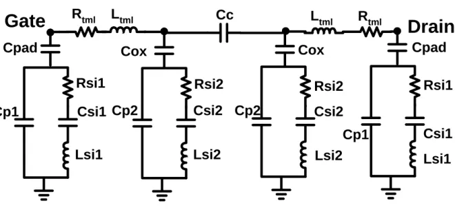
(26) β=. Weff ⋅ μeff ⋅ Cox Leff. a = 1−. VDS , VDSAT. = 0,. (2-33). Linear region. Saturation region. (2-34). and Gdsnoi is the thermal noise coefficient with default value equal to 1. Models mentioned above are integrated into various commercial simulators. Many other models have been proposed to consider velocity saturation effect, hot-electron effect or both [17, 18]. But they are not yet well accepted and verified. Noise simulation result comparison of different models was done in [19]. In this thesis, HSPICE model with NLEV set to 3 was used. BSIM4 Model There are two channel thermal noise model in BSIM4. One is a charge based model similar to that used in BSIM3v3.2 and the other is called the holistic model. These two model can be selected by setting the parameter tnoiMod [13]. The schematic for BSIM4 channel thermal noise model is shown in Fig. 2.3.. If tnoiMod =0 (charge based model) The noise current is given by. SId =. 4kT Δf .NTNOI L2eff Rds (V ) + μeff Qinv. (2-35). Where Rds(V) is the bias-dependent LDD source/drain resistance, and the parameter NTNOI is introduced to improve accuracy for fitting to short-channel devices.. If tnoiMod =1 (holistic model) 15.
(27) In this thermal noise model, all the short-channel effects and velocity saturation effect incorporated in the I-V model are automatically included and it explain the name given by “holistic” noise model. In this model, the amplification of the channel thermal noise through Gm and Gmbs as well as the induced-gate noise with partial correlation to the channel thermal noise are all captured in the new noise partition model (Fig .2.3). The noise voltage source partitioned to the source side is given by. v d 2 = 4kT θtnoi 2. Vdseff Δf Ids. (2-36). and the noise current source put in the channel region with gate and body amplification is expressed as. i d 2 = 4kT. Vdseff Δf [Gds + βtnoi .(Gm + Gmbs )]2 − v d 2 .(Gm + Gds + Gmbs )2 Ids. (2-37). where. θtnoi = RNOIB[1 + TNOIB.Leff .(. Vgsteff Esat Leff. )2 ]. (2-38). )2 ]. (2-39). and. βtnoi = RNOIA[1 + TNOIA.Leff .(. Vgsteff Esat Leff. where RNOIB and RNOIA are model parameters with default values 0.37 and 0.577 respectively. In the end of this thesis for future work, 90m RF-CMOS technology with BSIM4 model will be adopted and different noise models can be specified by setting tnoiMod. RF-CMOS at 90nm node and beyond will build the technology platform to support our future research work.. 16.
(28) 2.4 Flicker Noise Model BSIM-3 Model [13]. There are two flicker noise models available for selection in BSIM-3. One is SPICE2 flicker noise model and the other is BSIM-3 flicker noise model. The flicker noise model parameters were shown in the following table.. 1) SPICE2 model: K f IDS af SId = Cox Leff 2f ef. (2-40). where f is the frequency, Cox is the gate oxide capacitance. Leff is the effective channel length. 2) BSIM3 model: If |Vg s| > |Vth| + 0.1 (Vg s and Vth are positive for nMOS but negative for pMOS). SId = +. q 2 kT μeff Ids Cox Leff 2f ef .108. ⎡ ⎤ ⎡ N0 + 2 x10¹⁴ ⎤ Noic Noia .log + Noib.(No − N1 ) + (No 2 − N12 )⎥ ⎢ ⎢ 14 ⎥ 2 ⎣ N1 + 2 x10 ⎦ ⎣⎢ ⎦⎥. VtmIds ΔLclm Noia + Noib.N1 + Noic.N12 . Weff Leff 2f ef .108 (N1 + 2 x10¹⁴ )2. (2-41). 17.
(29) where Vtm is the thermal voltage, μeff is the effective mobility at the given bias condition. Leff and Weff are the effective channel length and width, respectively. No is the charge density at the source side given by. N0 =. Cox (Vgs − Vth ) (2-42). q. The parameter N1 is the charge density at the drain end given by. N1 =. Cox (Vgs − Vth − min(Vds ,Vdsat )) q. (2-43). ΔLclm is the channel length reduction due to channel length modulation and calculated by ⎧ ⎡ Vds − Vdsat ⎤ + Em ⎥ ⎪ ⎢ Litl ⎪⎪Litl .log ⎢ ⎥ ΔLclm = ⎨ Esat ⎢ ⎥ (forVds > Vdsat ) ⎢ ⎥ ⎪ ⎣ ⎦ ⎪ ⎪⎩0(otherwise ) (2-44) Esat = Otherwise. 2ν sat. μeff. , Litl = 3 X jTox. (|Vg s| |≦ |Vth| + 0.1) SId =. Slim it xSwi Slim it + Swi. (2-45). where Slimit is the flicker noise calculated at |Vg s| |= |Vth| + 0.1 and Swi is given by Swi =. NoiaV . tm .Ids 2 Weff Leff .f ef .4 x1036. (2-46). BSIM-4 Model [13]. There are two flicker noise models in BSIM-4. The parameter fnoimod is available to 18.
(30) specify which model to use. When fnoimod is set to 0, a simple flicker noise model, i.e. the SPICE2 model is invoked. As fnoimod =1 is specified, a unified physical flicker noise model is used. Basically, these two models follow those implemented in BSIM3v3, but there exist significant improvement on the unified model. For instance, the smooth transition over all bias regions is achieved and the bulk charge effect is considered in the improved model. For fnoiMod=0 (a simple model) KF .IDS AF SId = Coxe Leff 2f EF. (2-47). where f is device operating frequency. This model is the same as SPICE2 flicker noise model in BSIM3. Note that Coxe used in BSIM4 is different from Cox used in BSIM3. This change accounts for the fact that BSIM4 adopts the electrical oxide thickness for most of capacitance calculations, but BSIM3 does not distinguish between the physical and the electrical oxide thicknesses. For fnoiMod=1 (a unified model). This model involve both carrier number fluctuation and mobility fluctuation models, and take into account of the bulk charge effect. In the inversion region , the noise density is expressed as ⎡ ⎤ ⎛ N0 + N * ⎞ NOIC (No 2 − N12 )⎥ + NOIB.(No − N1 ) + ⎢NOIA.log ⎜ * ⎟ Coxe (Leff 2 ⎢⎣ ⎥⎦ ⎝ N1 + N ⎠ 2 2 kTVtmIds ΔLclm NOIA + NOIB.N1 + NOIC.N1 (2-48) . + 2 ef 8 (N1 + N * )2 Weff (Leff − 2.LINTNOI ) f .10. SId =. q 2 kT μeff Ids − 2.LINTNOI )2 Abulk f ef .1010. where Vtm is the thermal voltage, μeff is the effective mobility at the given bias condition, and Leff and Weff are the effective channel length and width, respectively. No is the charge density at the source side given by. 19.
(31) N0 =. CoxVgsteff q. (2-49). The parameter N1 is the charge density at the drain end given by CoxeVgsteff .(1 − N1 =. AbulkVdseff ) Vgsteff + 2v t. q. (2-50). N* is given by N* =. kT .(Coxe + Cd + CIT ) q2. (2-51). where CIT is a model parameter from DC I-V model and Cd is the depletion capacitance. In the subthreshold region, the noise power spectral density (PSD) is written as Sid ,subVt =. NOIA.kT .Ids 2 Weff Leff .f EF .N * .1010. (2-52). The total PSD of flicker noise is SId =. Sid ,inv xSid ,subVt Sid ,inv + Sid ,subVt. (2-53). 2.5 High Frequency Noise Measurement In this work, high frequency noise measurement was supported by Radio Frequency Technology Center of National Nano Device Laboratory (NDL RFTC). On-wafer noise characterization was conducted using NP5 series noise parameter measurement system. The 20.
(32) measurement system is introduced as follows. 2.5.1 System Configuration [20]. The configuration of a high frequency noise measurement system ATN-NP5B is shown with a simple block diagram in Fig. 2.4. This system basically consists of three sub-systems an ATN NP5B wafer probe test set, a vector network analyzer (VNA) - HP8510C, and a noise figure meter (NFA) - HP8970B. The NP5B system works as a switch for switching between the HP8510C for s-parameters measurement and the HP8970B for noise measurement in a two port network. The NP5B is comprised of a main controller unit, which drives the externally connected mismatch noise source (MNS) and remote receiver module (RRM). The MNS is a solid state electronic tuner with a built-in bias-T and RF switches, which serve to switch the connection between the DUT (device under test) to VNA and the noise source to the DUT. The DUT’s output is connected through RRM unit to either a VNA (8510C) or a NFA (HP8970B). Note that the RRM contains a bias-T, a low noise amplifier (LNA), and switches. The LNA adopted in RRM can drive the second stage to a lower noise and lower system noise figure. In this way, he noise measurement accuracy can be improved. Noise source is the noise power supply connected at port 1 defined by ENR (excess noise ratio) value, which contains a diode on under reverse bias. It can be operated at a hot or a cold state. When operating at a cold state, the diode was free from the external bias. At this time the noise is the room temperature noise and defined by a noise temperature Tc. When working at a hot state, the diode is subject to a reverse bias and contributes a higher noise defined by a noise temperature Th. The ENR of noise source can be calculated as. ENR(dB ) = 10 log(. Th − Tc ),T0 = 290K T0. 21. (2-54).
(33) 2.5.2 System Calibration and Measurement [21]. As high frequency characterization was conducted on the devices (DUT), the applied signals with short wavelength are comparable to the probe, cables, adapters, bonding wires, and DUT. Thus, losses caused by the mentioned connecting elements will seriously degrade the measurement accuracy and resolution, and the impact becomes particularly critical with increasing frequency.. On the other hand, a measurement system has its own system error. Consequently, a system calibration should be performed to take those losses into consideration. The standard procedure is to calibrate the system errors and then shift the measurement signal reference plane to the DUT plane. The validity and accuracy of the calibration results depend on the calibration method used. The calibration procedure is conducted through the following six steps. Following the system calibration, the RF probe must be probed on short, open, load, and thru dummy pad; in other calibration steps, the RF probe is probed on the same thru dummy pad. 1. Short, open, and load (SOL) calibration : Connected with a short, open, load in the place of the noise source on MNS to perform S22 measurement. This raw data will be combined with the data achieved through full two-port calibration to determine the s-parameters of the MNS. 2. Noise source calibration : First, connect the noise source to the MNS, which have established a reference plane from the SOL calibration. Then, make S-parameters measurement with the noise source at hot/cold to calculated the corresponding reflection coefficients and noise power for the noise source. This noise power measurement is used later to establish the gain and noise figure for the receiver. 3. S-parameters calibration : This step is a standard s-parameters calibration. There are many calibration. methods. like. short-open-load-thru. (SOLT),. line-reflect-match. (LRM),. thru-reflect-line (TRL). In this thesis, we used the SOLT calibration method. This calibration 22.
(34) step was conducted in order to shift the reference plane to the DUT plane, and later for the noise figure calculation. 4. Thru-delay calibration : Once the S-parameter calibration is finished, then system will check the thru delay automatically. For our currently measurement, the thru delay approximates 1ps. 5. RRM and MNS calibration : For MNS calibration, S22 measurement was carried out by changing the impedance states of the solid state tuner to calibrate the source reflection coefficients. These impedances are then referred to the S-parameters port 1 reference plan. For RRM calibration, S11 measurement was performed to determinate the input reflection coefficient of the receiver. This information is referred to the S-parameter port 2 reference plan. 6: System noise parameter calibration : In the last step, the noise power with varied source impedance is measured and the receiver noise parameters are stored at the port 2 reference plan. After calibration, noise measurement reference plane is then established. Before noise measurement, we can measure the noise figure on the thru pad to verify the calibration result. Theoretically, the thru pad didn’t contribute the noise. Therefore, the noise figure we measured must be less than 0.1dB. In the beginning of noise measurement, S-parameters measurement at the DUT reference plane should be done first. These S-parameters are necessary information for calculating noise parameters in next step. In the following, the electronic tuner (MNS) will vary the impedance to change the source reflection coefficient (Γs) around the Smith chart. Then the output noise power of DUT via the receiver as a function of Γs was measured. As a result, each individual Γs and its corresponding noise power construct a set of equations. Basically, Only four input states are needed for noise parameters characterization because the noise parameters calculation equation has only four unknown 23.
(35) parameters. In practice, in order to reduce the random system error, we usually measured more than four states, in our experience, we generally collect data from 24 or 32 states. Then a proper fitting procedure was performed to extract these four parameters. Finally, the four noise parameters: NFmin, Rn, Re(Γopt) or Re(Yopt) and Im (Γopt) or Im(Yopt) are obtained. In the measurement process, the overall noise figure was calculated by Y-factor method technique. The overall noise figure is then under a noise figure correction step to determine the noise figure of the DUT. Details of Y-factor method and noise figure correction are included in Appendix A.. 24.
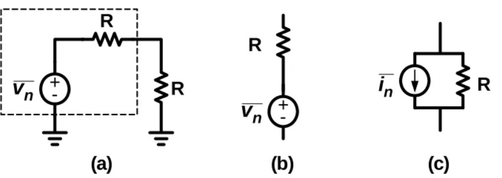
(36) R R. vn +-. R. vn +-. (a). in. (b). R. (c). Fig. 2.1 (a) Equivalent network for computing thermal noise of a resistor. (b)(c) Thermal noise model for a resistor.. W Gate L. QI (x). Source. Drain. v(x). E, lateral field. P-substrate. 0. x x+dx. Leff. Fig. 2.2 Schematic diagram of a MOSFET operated in saturation condition.. 25.
(37) (a). (b). Fig .2.3 Schematic for BSIM4 channel thermal noise modeling (a) tnoiMod=0 (b) tnoiMod=1. NP5 controller Noise figure meter HP8970 Noise figure test set Network analyzer HP8510 DC power supply HP4142. Noise source. Mismatch Noise Source (MNS). DUT. Remote Receiver Module (RRM). MNS: A solid state electronic tuner with embedded bias-T and switching circuit. RRM: A low noise amplifier with embedded bias-T and switching circuit. Fig. 2.4 Block diagram of ATN NP5B noise figure measurement system configuration.. 26.
(38) Chapter 3 Scalable Lossy Substrate Model for Various Pad Structures The original lossy substrate model proved the mechanism of excess noises caused by substrate loss coupled through the lossy pads [4-6]. In this chapter, an enhanced lossy substrate model is developed to accurately simulate RF noise for on-chip devices with freedom in pad and TML (transmission line) layouts. This new lossy substrate model is composed of two parallel and series RLC networks in series with Cpad and Cox to model the capacitive coupling through the GSG pads and TML from the low resistivity silicon substrate. The precise distribution of lossy substrate effect between that through the pads and the remaining portion through TML realizes accurate prediction of S-parameters and noise parameters for miniaturized devices over broadband regime.. 3.1 GSG Pad Layout Structures In order to study lossy substrate effect on high frequency noise and the excess noise induced through pad and TML, various GSG pad structures such as lossy, normal, and small pads with different metal topologies or pad sizes were fabricated by 0.13um Cu/FSG BEOL (Back-End-Of-Line) process to investigate the resulted lossy substrate effect. Fig. 3.1.(a) and (b) illustrate the 3D schematics for lossy and normal pads in which the ground pads (G) were constructed with stacked metals from the bottom (M1) to the top (M8) while the signal pads (S) were built with two different schemes. For lossy pad scheme in Fig. 3.1.(a), the S pad are composed of stacked metals from M2 to M8, whereas for normal pad scheme in Fig. 3.1.(b), they are consisted of top metal (M8) only and excluding all lower metals. As for small pad scheme, its signal pads just follow that of normal pad scheme but with smaller size of 50umx35um w.r.t. 50umx50um for normal and lossy ones. All three pad structures adopt exactly the same G pad scheme. 27.
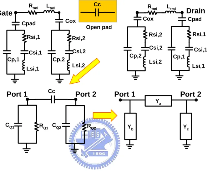
(39) 3.2 Lossy Substrate Model Development for Various Pad Structures Before we study lossy substrate effect on high frequency noise and the excess noises, which were introduced through pad and TML, the open pad equivalent circuit model should be developed first. Fig. 3.2. depicts the equivalent circuit schematics of the enhanced lossy substrate model to incorporate various pad structures. This new RLC network was created to accurately capture the frequency response with varying pad structures associated with the lossy substrate. The primary enhancement to the original model is a modification on the substrate RLC network in conjunction with TML by adopting a Cox representing the TML to substrate coupling capacitance. The resulted enhanced model is composed of two substrate RLC networks in series with Cpad and Cox to simulate substrate loss through the pads and TML from silicon substrate, respectively. These capacitances are mainly governed by the signal pad or TML area and metal stack underneath. In this work, these two capacitances are physical parameters calculated based on layout and BEOL process parameters (metal thickness, IMD thickness and dielectric constants) rather than from extraction. Csi and Lsi in series with Rsi make this RLC network different from the conventional substrate network by a simple shunt RC. Capacitances Cp and Csi account for the capacitive coupling while substrate resistance Rsi and inductance Lsi were proposed to model the semi-conducting nature of silicon substrate under high frequency operation. Coupling capacitance Cc connecting the two-ports is required to model S12 and S21 of the open pads and it should be removed from the pad model when a device is attached through the two-ports to simulate S-parameters and noise parameters of a full structure before de-embedding. Regarding the resistance (Rtml) and inductance (Ltml) associated with transmission line, they can be extracted from Z-parameters of a short pad after modified open de-embedding. A complete extraction flow assisted by equivalent circuit analysis can be referred to our original work [4-5]. Fig. 3.3. illustrates the schematic block diagram derived by circuit analysis theory to extract the circuit elements (Rsi, Csi, Lsi, Cp, RTML, and LTML). Note that this model parameters extraction method just serves as the initial 28.
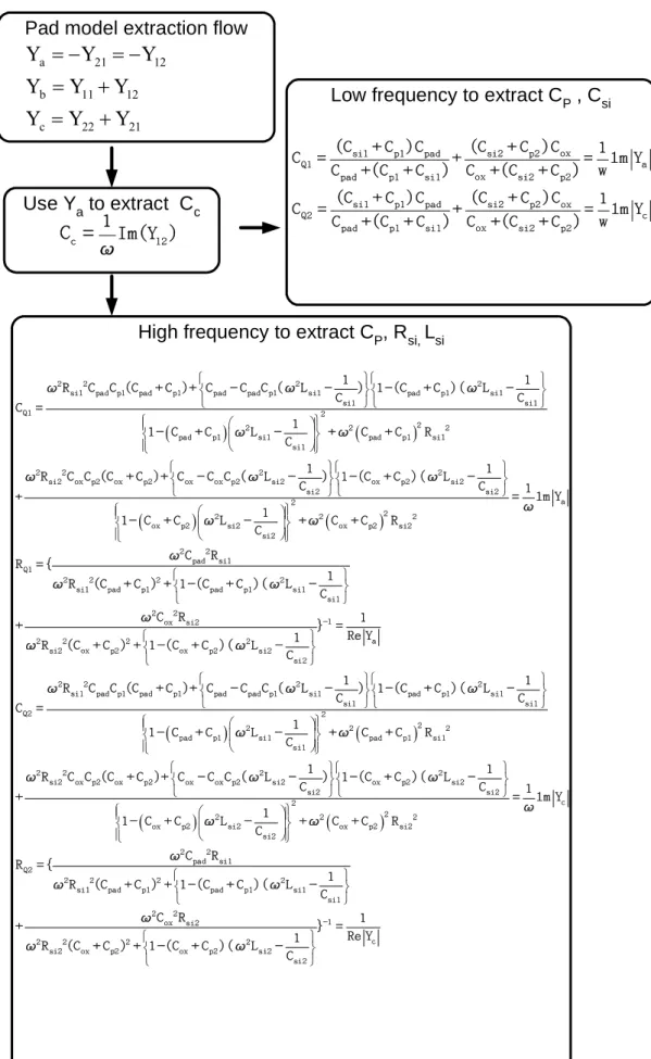
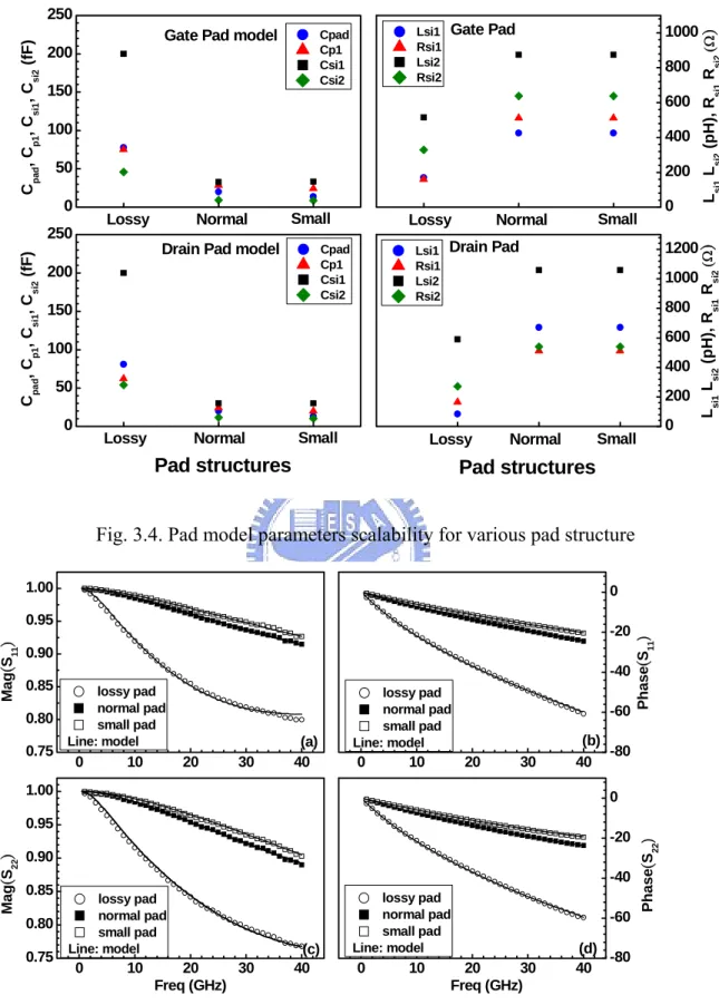
(40) values for further optimization. Parameters optimization was done by Agilent IC-CAP and Agilent Advance Design System (ADS) to get the best fit to S- and Y-parameters. The table 3.1 lists full set of model parameters through optimization for lossy, normal, and small pads respectively. We could observed something interesting from the parameters of lossy substrate model for various pad structures. The category of lossy pad reveals apparently larger capacitances for all three elements(Cpad, Cp1, Csi1) and lower resistance (Rsi1) and inductance (Lsi1) in the first RLC network under pad and larger Csi2 and lower Rsi2, Lsi2 under the second RLC network under TML. As shown in Fig. 3.4. The large capacitances indicated the much coupled effect from the lossy substrate, and the lower resistances and inductances implied that the low resistivity Si substrate effect. Note that Cox is kept at similar value for all three kinds of pad due to the same metal layout and topology for TML from the pads to intrinsic device. On the other hand, Cpad presents significant difference among the three pad structures in which the scaling factors of around 3.9~4 for lossy versus normal and 0.82~0.85 for small versus normal just approach the theoretical values of 4.04 and 0.75 calculated by layout and process parameters. The accuracy of optimized lossy substrate model was verified and justified by good match with measured S11 and S22 (mag. and phase ) for lossy, normal, and small pads together in Fig. 3.5. Good prediction was achieved for Y-parameters simultaneously (real and imagine part of Y11 and Y22 ) as shown in Fig. 3.6. We could observed something interesting that the lossy pad reveals remarkably smaller magnitudes and more negative phase for both S11 and S22,extraordinary shift in magnitude and phase away from 1.0 and 0° under increasing frequency. We have been known that the purely capacitive plot on Smith chart was trended to along the side of smith chart and kept the constant R circle (kept the same magnitudes), which started form the point of Γ=1 on smith chart. The lossy pad revealed remarkably smaller magnitudes indicated there were not only capacitances but also some parasitic components like resistances and inductances in lossy substrate model to characterize this lossy effect, and the more negative phase indicated the larger capacitances. We could observed these effects 29.
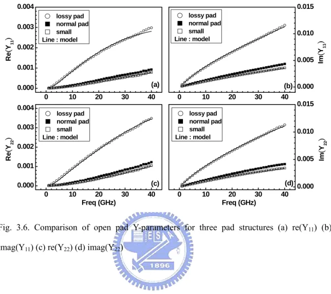
(41) obviously from Y-parameters which larger Im(Y11) indicated larger capacitances in the lossy pad. The difference between normal and small pads is much smaller. As a result, the enhanced lossy substrate model can accurately simulate the pad structure effects in terms of layout and metal topologies with predictable scaling factors.. 30.
(42) G. S. G. M8. M8. M8. Rtml, Ltml Cpad M7~M2 Cox. M7~M2. M1 DUT Substrate Rsi Csi r. Cp. Lsi. (a). G. S. G. M8. M8. M8. Rtml, Ltml M7~M3 M7~M2 Cox M2 DUT. M7~M2 M1. Cpad Substrate Rsi Csi r. Cp. Lsi. (b) Fig .3.1. 3D schematics of GSG pads (a) lossy pad scheme : S-pads with stacked metals from M2 to M8 (b) normal pad:S pads with top metal (M8) only. 31.
(43) Rtml. Gate Cpad. Ltml. Cc. Rtml. r. Drain Cpad. Cox. Cox. Cp1. Ltml. r. Rsi1. Rsi2. Rsi2. Csi1 Cp2. Csi2 Cp2. Csi2. Rsi1. Csi1. Lsi2. r. Lsi2. r. Lsi1. r. r. Cp1. Lsi1. Fig. 3.2. The equivalent circuit schematics of enhanced lossy substrate open pad model. 32.
(44) Rtml. Cc. Ltml. Drain. r. Cpad. Open pad. Csi,2. Csi,2. Csi,1. Cp,2. r. r. r. Cp,2 Lsi,1. Cc. Rsi,1. Rsi,2. Rsi,2. Lsi,2. Port 2. Lsi,2. Csi,1 Cp,1. Port 1. r. Rsi,1. Port 1. Ltml. Cox. Cox. Cpad. Cp,1. Rtml. r. Gate. Lsi,1. Port 2 Ya. CQ1. RQ1 CQ2. RQ2. Yb. Fig. 3.3 (a) Equivalent circuit model derivation by circuit analysis. 33. Yc.
(45) Pad model extraction flow. Ya = −Y21 = −Y12 Yb = Y11 + Y12. Low frequency to extract CP , Csi. Yc = Y22 + Y21. Use Ya to extract Cc 1 Cc = Im(Y12 ) ω. C Q1 =. (Csi1 + C p1 )C pad (C + C )C 1 + si2 p2 ox = lm Ya C pad +(C p1 + Csi1 ) Cox +(Csi2 + C p2 ) w. C Q2 =. (Csi1 + Cp1 )C pad (C + C )C 1 + si2 p2 ox = lm Yc C pad +(Cp1 + Csi1 ) Cox +(Csi2 + C p2 ) w. High frequency to extract CP, Rsi, Lsi ⎧. ω2 R si12 C pad C p1(C pad + C p1 )+ ⎨C pad - CpadC p1(ω2 L si1 C Q1 =. ⎩ 2 ⎧⎪ ⎛ 2 2 1 ⎞ ⎫⎪ 2 2 ⎨1 - ( C pad + C p1 ) ⎜ω L si1 ⎟ ⎬ +ω ( C pad + Cp1 ) R si1 C si1 ⎠ ⎭ ⎪ ⎝ ⎩⎪ ⎧. ω2 R si22 C ox Cp2(C ox + C p2 )+ ⎨C ox - Cox Cp2(ω2 Lsi2 ⎩. +. 1 ⎫⎧ 1 ⎫ )⎬ ⎨1 -(C pad + C p1 )(ω2 L si1 ⎬ Csi1 ⎭ ⎩ Csi1 ⎭. ⎛ 2 1 ⎪⎧ ⎨1- ( C ox + C p2 ) ⎜ω L si2 Csi2 ⎪⎩ ⎝. 2. 1 ⎫⎧ 1 ⎫ )⎬ ⎨1 -(C ox + C p2 )(ω2 Lsi2 ⎬ Csi2 ⎭ ⎩ Csi2 ⎭. ⎞ ⎪⎫ 2 2 2 ⎟ ⎬ +ω ( C ox + C p2 ) R si2 ⎠ ⎪⎭. =. 1 lm Ya ω. ω2 C pad2 R si1 R Q1 = { ⎧ 1 ⎫ ω2 R si12(C pad + C p1 )2 + ⎨1 -(C pad + C p1 )(ω2 Lsi1 ⎬ Csi1 ⎭ ⎩ +. ω2C ox2 Rsi2 ⎧ 1 ⎫ ω2 R si2 2(Cox + C p2 )2 + ⎨1 -(Cox + C p2 )(ω2 Lsi2 ⎬ C si2 ⎭ ⎩. }-1 =. ⎧. ω2 R si12 C pad C p1(C pad + C p1 )+ ⎨Cpad - Cpad C p1(ω2 L si1 C Q2 =. ⎩. 2. 1 ⎫⎧ 1 ⎫ )⎬ ⎨1 -(C pad + C p1 )(ω2 Lsi1 ⎬ Csi1 ⎭ ⎩ Csi1 ⎭. ⎧⎪ ⎛ 2 2 1 ⎞ ⎫⎪ 2 2 ⎨1 - ( C pad + C p1 ) ⎜ω L si1 ⎟ ⎬ +ω ( C pad + C p1 ) R si1 C si1 ⎠ ⎭ ⎪ ⎝ ⎩⎪ ⎧. ω2 R si22 C ox Cp2(Cox + C p2 )+ ⎨C ox - Cox C p2(ω2 L si2 +. 1 Re Ya. ⎩. 2. 1 ⎫⎧ 1 ⎫ )⎬ ⎨1 -(Cox + C p2 )(ω2 L si2 ⎬ C si2 ⎭ ⎩ Csi2 ⎭. ⎛ 2 2 1 ⎞ ⎪⎫ ⎪⎧ 2 2 ⎨1 - ( Cox + C p2 ) ⎜ω L si2 ⎟ ⎬ +ω ( Cox + C p2 ) R si2 C si2 ⎠ ⎪ ⎝ ⎩⎪ ⎭. =. ω2 C pad2 R si1 R Q2 = { ⎧ 1 ⎫ ω2 R si12(C pad + C p1 )2 + ⎨1 -(Cpad + C p1 )(ω2 Lsi1 ⎬ Csi1 ⎭ ⎩ +. ω2 C ox2 Rsi2 ⎧ 1 ⎫ ω2 R si22(Cox + C p2 )2 + ⎨1 -(Cox + C p2 )(ω2 Lsi2 ⎬ C si2 ⎭ ⎩. }-1 =. 1 Re Yc. Fig. 3.3 (b) Pad model parameter extraction flow 34. 1 lm Yc ω.
(46) Table 3.1 Pad model parameters for various pad structures Gate Pad RLC model parameters Pad layout Cpad (fF) Cp1 (fF) CSi1 (fF) LSi1 (pH) Lossy 77.87 74.97 200 170.7 20 28.55 32.68 425.3 Normal 13.89 24.43 33.4 425.3 Small Cp2 (fF) CSi2 (fF) LSi2 (pH) Pad layout Cox (fF) 10.78 1.629 Lossy 45.98 515.4 9.932 2.553 9.316 874.3 Normal 9.913 2.635 8.741 874.3 Small. RSi1 (Ω) 159.9 511.7 511.7 RSi2 (Ω) 328.8 638.3 638.3. Ltml (pH). Rtml (Ω). 50. 0.2. Drain Pad RLC model parameters Pad layout Cpad (fF) Cp1 (fF) CSi1 (fF) LSi1 (pH) Lossy 80.99 62 200 83.72 20.17 24.05 30 671.3 Normal 12.84 19.72 30 671.3 Small Cp2 (fF) CSi2 (fF) LSi2 (pH) Pad layout Cox (fF) 11.07 2 Lossy 54.15 590.6 10.21 2.887 11.73 1059 Normal 9.932 2.635 10.29 1059 Small. RSi1 (Ω) 164.3 511.7 511.7 RSi2 (Ω) 270.9 540.3 540.3. Ltml (pH). Rtml (Ω). 50. 0.2. 35. Cc (fF) 1.103.
(47) 150. Gate Pad. 1000 800 600. 100. 400. 50. 200. 0. Normal. Lossy. 250 Cpad, Cp1, Csi1, Csi2 (fF). Lsi1 Rsi1 Lsi2 Rsi2. Cpad Cp1 Csi1 Csi2. Small. Drain Pad model. Cpad Cp1 Csi1 Csi2. 200. Lsi1 Rsi1 Lsi2 Rsi2. 0. Small. Normal. Lossy. Drain Pad. 1200 1000 800. 150. 600. 100. 400 50. 200. 0. Normal. Lossy. Small. Lsi1 Lsi2 (pH), Rsi1 Rsi2 (Ω). Gate Pad model 200. Lsi1 Lsi2 (pH), Rsi1 Rsi2 (Ω). Cpad, Cp1, Csi1, Csi2 (fF). 250. Lossy. Pad structures. 0. Small. Normal. Pad structures. Fig. 3.4. Pad model parameters scalability for various pad structure 1.00. -20. 0.90 -40 0.85 0.80 0.75. lossy pad normal pad small pad Line: model. 0. 10. 20. 30. (a) 40. lossy pad normal pad small pad Line: model. 0. 10. -60 20. 30. 1.00. 0. 0.95 Mag(S22). (b) -80 40. -20. 0.90 0.85 0.80 0.75. -40 lossy pad normal pad small pad Line: model. 0. 10. 20 30 Freq (GHz). (c) 40. lossy pad normal pad small pad Line: model. 0. 10. 20 30 Freq (GHz). -60. Phase(S22). Mag(S11). 0.95. Phase(S11). 0. (d) -80 40. Fig. 3.5. Comparison of open pad S-parameters between measurement and lossy substrate model for three pad schemes, lossy normal, and small (a) mag(S11) (b) phase(S11) (c) mag(S22) (d) phase(S22) 36.
(48) 0.004. 0.010. 0.002 0.005. Im(Y11). Re(Y11). 0.003. 0.015 lossy pad normal pad small Line : model. lossy pad normal pad small Line : model. 0.001 (a) 0 0.004. Re(Y22). 0.003. 10. 20. 30. 40. 0. 10. 20. 30. lossy pad normal pad small Line : model. lossy pad normal pad small Line : model. (b) 0.000 40 0.015. 0.010. 0.002 0.005. Im(Y22). 0.000. 0.001 (c). 0.000 0. 10. 20 30 Freq (GHz). 0. 40. 10. 20 30 Freq (GHz). (d) 0.000 40. Fig. 3.6. Comparison of open pad Y-parameters for three pad structures (a) re(Y11) (b) imag(Y11) (c) re(Y22) (d) imag(Y22). 37.
(49) Chapter 4. RF MOSFET Intrinsic I-V and C-V Model Calibration 4.1 I-V and C-V Modeling Theory Valid for Sub-100nm MOSFETs It is very important and required pre-works to create an accurate current-voltage (I-V) and capacitance-voltage (C-V) model for RF MOSFET model development. A complete model of I-V characteristic over a wide bias range is important for nowadays circuit design, especially for analog and RF circuit design, where a variety of bias conditions will be used. Also with the rapidly increases demand for ultra-low power circuit design in recent year, an accurate model near subthreshold region is also necessary. An accurate capacitance model is also required to predict the devices or circuit speed and AC performance. In conclusion, correct I-V and C-V models are essentials to provide us trustworthy DC and AC characteristics for further study of high frequency performance. In our research, Bsim3v3 model [13] is used which releases by foundry, TSMC for 0.13um MS/RF CMOS general purpose 1P8M 1.2V technology. In this thesis, there are three dimension of devices which keep width with 4um and length with 0.13um by various finger numbers of NF=18, 36, 72, were adopted for I-V , C-V and S-parameters model calibration and extended to high frequency noise model development. Multi-finger structure was employed to reduced gate resistance and the induced excess noise, and then further to investigate the impact on high frequency and noise performance as well as model scalability to fit various device geometries. The model calibration work was started by modifying the model parameters in Bsim3v3 model. Before this work, DC I-V and two port S-parameters were measured by Agilent vector network analyzer up to 40GHz. Y- and H- parameters can be derived from S-parameters for extraction of gate capacitances (Cgg, Cgs, Cgd) and current gain 38.
(50) cut-off frequency fT. The ultimate goal is to build a accurate model by Bsim3v3 model calibration which can be correspond to the measured results on I-V, C-V, S-parameters, and noise performance. Before starting the model parameters calibration and optimization, we must be known some process related model parameters are specified and fixed at their known values, such as some important geometry or process parameters, Lint (channel length offset), Wint (channel width offset), Tox (oxide thickness), Nch (channel doping concentration), Xj. (junction depth) and so forth. For sub-100nm MOSFET, the following important mechanisms are considered in Bsim3v3 model (1) short channel and narrow width effects on threshold voltage, (2) mobility reduction due to vertical field, (3) velocity saturation, (4) drain-induced barrier lowering (DIBL), and (5) Substrate current induced body effect (SCBE). It is assumed that most of the I-V and C-V parameters were fairly modeled in the original model and only minor modification is needed to improve the model accuracy.. 4.2 DC I-V Model Development For RF MOSFET, 3–terminal test structure is usually implemented with common source configuration in which source and body terminals are tied together and grounded. To measure its high frequency characteristic (both S parameter and NFmin), two sets of probing pad with G-S-G structures are implemented and connected to the gate and drain terminals. The parasitic resistances associated with MOSFET’s terminals such as Rg_ext, Rd_ext, Rs_ext, and Rb_ext contributed from the interconnection lines and probing pads will affect I-V characteristic of DUT. In I-V model development, these parasitic resistances can not be moved out. Extraction of these parasitic resistances should be done and added to the original intrinsic MOSFET model (BSIM3). These parasitic resistances such as Rd_ext and Rs_ext will cause the measured drain current degradation. Rd_ext at drain terminal will affect the rising slope between linear and saturation region, and Rs_ext at source terminal will affect the drain current at saturation region and also cause the transconductance (gm) degradation. Rg_ext at 39.
數據
+7
相關文件
Hence on occupation category, total manpower requirement for managers and administrators, professionals and associate professionals taken together is projected to grow at an
“More Joel on Software : Further Thoughts on Diverse and Occasionally Related Matters That Will Prove of Interest to Software Developers, Designers, and Managers, and to Those
When renaming a file without changing file systems, the actual contents of the file need not be movedall that needs to be done is to add a new directory entry that points to
The major testing circuit is for RF transceiver basic testing items, especially for LNA Noise Figure and LTE EVM test method implement on ATE.. The ATE testing is different from
To explore and improve accuracy of the existing biaxial rectangular robot, the research uses two linear scales to measure the positioning errors of the two axes.. After that,
在軟體的使用方面,使用 Simulink 來進行。Simulink 是一種分析與模擬動態
我們分別以兩種不同作法來進行模擬,再將模擬結果分別以圖 3.11 與圖 3.12 來 表示,其中,圖 3.11 之模擬結果是按照 IEEE 802.11a 中正交分頻多工符碼(OFDM symbol)的安排,以
針對 WPAN 802.15.3 系統之適應性柵狀碼調變/解調,我們以此 DSP/FPGA 硬體實現與模擬測試平台進行效能模擬、以及硬體電路設計、實現與測試,其測 試平台如圖 5.1、圖
