國
立
交
通
大
學
電子工程學系 電子研究所
碩 士 論 文
應用於射頻/類比電路的三氧化二鑭
金屬-絕緣層-金屬電容之特性研究
Study on Lanthanum Oxide Metal-Insulator-Metal
Capacitor for Radio-Frequency/Analog Applications
研 究 生:吳 杼 樺
指導教授:邱 碧 秀 博士
應用於射頻/類比電路的三氧化二鑭
金屬-絕緣層-金屬電容之特性研究
Study on Lanthanum Oxide Metal-Insulator-Metal
Capacitor for Radio-Frequency/Analog Applications
研 究 生:吳 杼 樺 Student:Shu-Hua Wu
指導教授:邱 碧 秀 博士 Advisor:Dr. Bi-Shiou Chiou
國 立 交 通 大 學
電子工程學系 電子研究所
碩 士 論 文
A Thesis
Submitted to Department of Electronics Engineering and Institute of Electronics
College of Electrical and Computer Engineering National Chiao Tung University
in Partial Fulfillment of the Requirements for the Degree of Master
in
Electronics Engineering
September 2009
Hsinchu, Taiwan, Republic of China
應用於射頻/類比電路的三氧化二鑭
金屬-絕緣層-金屬電容之特性研究
研 究 生: 吳 杼 樺 指導教授: 邱 碧 秀 博士
國 立 交 通 大 學
電子工程學系 電子研究所
摘 要
在本篇論文中,我們使用高介電常數的三氧化二鑭絕緣層,來製作應用於高頻或類 比電路的低溫金屬-絕緣層-金屬(金氧金)電容。然後深入探究其操作原理,和實際應用 面上所產生的問題,包含漏電流和其傳導機制、類比特性和其訊號失真機制、受電應力 行為和劣化過程,以及介電絕緣層崩潰和可靠度特性探討等。 首先,就三氧化二鑭絕緣層電流的傳導機制而言,它不像傳統二氧化矽絕緣層般, 有這麼明確的載子傳輸行為。因為此三氧化二鑭介電質屬於低溫製備,擁有許多的缺陷 密度和介面態在能隙中,致使其傳導機制較複雜且需要被修正。第二,此三氧化二鑭金 氧金電容的電容密度與外加電壓、溫度和頻率之間的關係亦在此論文中詳加探討。有鑑 於過往研究對描述這些關係之背後成因的論點分歧,我們從高介電常數絕緣層最根本的 介電行為:極化與鬆弛的角度來切入。於是歸結出,電容的電壓係數主要受空間電荷的 極化與鬆弛影響,而電容的溫度係數則最主要受控於電偶極的極化和鬆弛行為。而此電 容在定電壓應力測試中,因為電應力會造成缺陷的產生,進而降低空間電荷的遷移率, 導致其電容的電壓係數降低。反之,缺陷引發的電偶極極化效應則促使電容的溫度係數 增加。由此可進一步證實,這兩種機制主宰了高介電常數金氧金電容之類比特性的精確 度。 接下來,我們討論此三氧化二鑭金氧金電容之電應力行為及其時間依存性可靠度的 分析。由實驗結果可歸納得,三氧化二鑭金氧金電容在定電壓應力下的劣化機制是缺陷產生與電荷補捉,這可借由量測低電場中的應力誘生漏電流及偵測出應力貢獻的電容密 度變化來分別確定。我們也觀察到三氧化二鑭金氧金電容在定電壓應力下的二階段時間 依存性崩潰現象,這歸因於金屬與介電質間的界面層先崩潰並導致劇烈的電荷補捉與釋 放效應,爾後介電質本體也隨之崩潰。這層不可避免的界面層是因高介電常數介電薄膜 直接沉積在金屬表面上所形成,由於它原本就具有較高的缺陷密度而易於崩潰,於是當 介電層微縮時因它的不可微縮性就變成一個可靠度的問題。是故,界面層較高的初始缺 陷密度不僅影響金氧金電容的漏電流和類比特性,在元件失效上亦佔有舉足輕重的地 位。 最後,本實驗所製作的低溫十奈米三氧化二鑭金氧金電容,其具有低漏電流(在外 加電壓−1 V時為 9.4 nA/cm2 ),很高的崩潰電場 (在25 °C時大於 7 MV/cm),低的電容 電壓係數(頻率在100 kHz時為 671 ppm/V2),足夠高之電容密度(11.4 fF/μm2),以及高 度穩定性和良好的可靠度等眾多優良特性。因此,鑭系高介電常數絕緣層金氧金電容是 超大型積體電路技術中後段的射頻和類比電路裡最具潛力的被動元件。
Study on Lanthanum Oxide Metal-Insulator-Metal
Capacitor for Radio-Frequency/Analog Applications
Student:Shu-Hua Wu Advisor:Dr. Bi-Shiou Chiou
Department of Electronics Engineering and Institute of Electronics
College of Electrical and Computer Engineering
National Chiao Tung University
Abstract
In this study, the low-temperature metal-insulator-metal (MIM) capacitor with the high dielectric constant (high-k) lanthanum oxide (La2O3) film deposited by electron beam (e-beam)
evaporation was fabricated and characterized for radio frequency (RF) and analog applications. The operational principles and the implementation issues of the high-k La2O3
MIM capacitor are discussed, including leakage current and conduction mechanisms, analog properties and distortion mechanisms, stress behaviors and degradation processes, as well as dielectric breakdown and reliability characteristics.
To begin with, we evaluate the conduction mechanisms for high-k La2O3 MIM
capacitors. Unlike the conventional SiO2 MIM capacitor where the quantum-mechanical
tunneling is pronounced, the trap-related mechanisms are important for high-k MIM capacitors with low temperature fabrication, due to the high trap and interface state density in the high-k dielectric. Secondly, the effects of voltage, temperature, and frequency on the capacitance of high-k La2O3 MIM capacitors are investigated in detail on the basis of
fundamental high-k dielectric behaviors: polarization and relaxation. The space charge polarization and relaxation are principally responsible for the positive voltage coefficient of capacitance (VCC). However, the dipolar polarization and relaxation dominate the positive
temperature coefficient of capacitance (TCC). Interplay of these two effects on analog characteristics is crucial for developing the precise MIM capacitors with high-k dielectrics. The changes in VCC and TCC caused by the constant voltage stress (CVS) also verify the above inferences. VCC decreases since the space charge mobility reduced by stress induced traps, but TCC increases because the quantity of trap induced dipoles grows during stress.
Furthermore, the stress behaviors and the reliability issues of high-k La2O3 MIM
capacitors under various CVS conditions are also studied. The wear-out mechanisms of La2O3
MIM capacitors during electrical stress are trap generation and charge trapping. This could be identified by measuring the stress induced leakage current (SILC) at low field and by detecting the capacitance variation under electrical stress, respectively. Moreover, the very distinct two-step time-dependent dielectric breakdown caused by CVS testing could be observed. It is ascribed to firstly the interfacial layer (IL) breakdown leading to the severe charge trapping/detrapping, followed by the breakdown of the bulk high-k layer. Therefore, the high intrinsic defect density in the IL not only affects the leakage current and analog characteristics of MIM capacitors, but also plays an important role on the device failure rate.
In summary, a highly stable and reliable 10-nm La2O3 MIM capacitor with low leakage
current (9.4 nA/cm2 at −1 V), high breakdown strength (> 7 MV/cm at 25 °C), small VCC (671 ppm/V2 at 100 kHz), low thermal budget (≤ 400 °C), and sufficient high capacitance density (11.4 fF/μm2) has been successfully demonstrated. The results highlight the promise
of the La-based high-k MIM capacitors as the next-generation passive component in RF/analog circuits.
A
CKNOWLEDGEMENTS 研究所兩年的生涯中,首先要感謝我的指導老師邱碧秀教授,老師的諄諄教誨以 及嚴謹認真的專業態度,總讓我受益匪淺。除了在專業知識上給我許多教導,老師的待 人處事更是我學習的典範,讓我一輩子受益良多。還要謝謝口試委員雷添福教授、侯拓 宏教授、吳文發博士的建議與協助,使我的論文更完整。 而我也要感謝實驗室的學長鄧至剛,不但給予我許多機台上的指導與訓練,而且把 他很多寶貴的經驗傳授給我。每當我在實驗上遇到任何困難,他總是先擱置自己的實驗 和研究,耐心與我討論問題並尋求解決。讓我終於得以完成學業。 另外,也要謝謝其他實驗室的學長、同學這兩年來對我的指導與幫助。包括張國 明教授實驗室的黃菘宏學長、林詩帆學長、廖彥凱同學、曾憶雯同學以及其他許多幫忙 我的同學。荊鳳德教授實驗室的張明峰學長與其他學長。羅正忠教授實驗室的陸冠文學 長、李勝凱學長及其他的學長和同學。崔秉鉞教授實驗室的徐曉萱學姐與其他學長。雷 添福教授實驗室的黃俊嘉學長及其他的學長們。材料所的呂佳凌學姐。以及長庚電子的 沙沙同學、阿信同學。逢甲電子的周美媛同學、廖峻偉同學。謝謝你們!也謝謝其他更 多幫助過我的人。 最後,感謝我的家人對我的支持與包容,讓我能夠完成碩士學位。父親吳水欽先生、 母親林郁郁小姐、大姐美瑤、二姐筱娟、大弟本元、二弟本丞,也把這本論文獻給你們, 謝謝!Contents
Abstract (Chinese) --- i
Abstract (English) --- iii
Acknowledgements --- v
Contents --- vi
List of Tables --- ix
Figures Caption --- x
Chapter 1 Introduction --- 1
Chapter 2 General Backgrounds and Literatures Review --- 7
2.1 Conduction Mechanisms in High-k Dielectrics --- 7
2.1-1 Schottky Emission --- 8
2.1-2 Poole-Frenkel Emission --- 9
2.1-3 Space-Charge-limited Current --- 11
2.1-4 High Trap Density Related Conduction --- 14
2.2 Dielectric Polarization and Relaxation of High-k MIM Capacitors --- 15
2.2-1 Dielectric Polarization --- 15
2.2-2 Dielectric Relaxation --- 17
2.3 Stress Behaviors of MIM Capacitors --- 19
2.4 Reliability Characteristics of MIM Capacitors --- 21
2.4-1 A Brief History on Reliability Improvement of Silicon-Related Device 21 2.4-2 Reliability Issues on MIM Capacitors --- 22
Chapter 3 Fabrication and Characterization Methods --- 32
3.1 Fabrication of La2O3 MIM Capacitor --- 32
3.2 Measurement and Parameters Extraction --- 34
3.3 Material Analyses --- 39
Chapter 4 Results and Discussion --- 47
4.1 Basic Properties of the E-beam Evaporated La2O3 Dielectric Films of MIM Capacitors --- 48
4.2 Leakage Current and Conduction Mechanisms of La2O3 MIM Capacitors ---- 49
4.3 Effects of Voltage, Temperature, and Frequency on The Capacitance of La2O3 MIM Capacitors --- 52
4.3-1 Characteristics of Voltage Coefficient of Capacitance --- 53
4.3-2 Characteristics of Temperature Coefficient of Capacitance --- 55
4.3-3 Characteristics of Frequency Coefficient of Capacitance --- 56
4.3-4 Summary--- 57
4.4 Behaviors of La2O3 MIM Capacitors Under Constant Voltage Stress --- 58
4.4-1 The Variation in Leakage Current --- 58
4.4-2 The Variation in Capacitance --- 60
4.4-3 The Variation in α and in TCC --- 61
4.4-4 Summary --- 63
4.5 Breakdown and Reliability Characteristics of La2O3 MIM Capacitors --- 63
4.5-1 Characteristics of Time-Zero Dielectric Breakdown --- 64
4.5-2 Characteristics of Time-Dependent Dielectric Breakdown --- 65
Chapter 5 Conclusions and Future Prospects --- 90
5.1 Conclusions --- 90
5.2 Future Prospects --- 92
References --- 96
List of Tables
Table 1-1 The empirical data about dielectric constant, energy bandgap, and conduction
band offset with respect to the Si of various high-k dielectrics [22]. --- 6
Table 1-2 Requirements for RF MIM capacitors according to ITRS [32]. --- 6
Table 2-1 Theoretical expressions of the bulk-limited conduction processes [44]-[50]. --- 29
Table 2-2 Theoretical expressions of the electrode-limited conduction processes in oxides
[46], [48]-[51] --- 30
Table 2-3 Comparison of Schottky-emission and Poole-Frenkel emission. --- 31
Table 5-1 Some recommendations for improving VCC and TCC without reducing the
capacitance density. --- 94
Table 5-2 Comparison on electrical characteristics of MIM capacitors with various high-k
Figures Caption
Fig. 1-1 The bandgap as a function of dielectric constant for various candidate oxides
[21]. --- 5
Fig. 1-2 Energy bandgap versus various rear-earth metal oxides (REOs) [33]. --- 5
Fig. 2-1 Energy-band diagram between a metal surface and a vacuum. Conduction band
edge means the vacuum energy level which is zero in electron energy. x0 is
introduced due to the singular point of image potential at x=0 [39]. --- 24
Fig. 2-2 Thermionic conduction (Poole-Frenkel conduction ) [39]. --- 24
Fig. 2-3 Restoring force on escaping electron. (a) The Schottky effect. (b) The
Poole-Frenkel effect. [39]. --- 25
Fig. 2-4 Thermal and quasi-thermal equilibrium (steady-state) of electrons in conduction
band Ec and trap level Et. F denotes quasi-Fermi level and the subscript 0 means
the thermal equilibrium [83]. The equilibrium states can be achieved by low injection and low internal emission. --- 25
Fig. 2-5 Mobility of electrons as a function of energy showing mobility gap (amorphous
stste) [84]-[86]. --- 26
Fig. 2-6 Energy diagram illustrating virtual cathode, cathode region, and anode region
under space-charge-limited conduction. λm denotes the position of virtual
cathode in the insulator [83]. The insulator is assumed to be free of surface states and ohmic contacts. --- 26
Fig. 2-7 Typical current by SCLC in (a) logarithmic scale and (b) semi-logarithmic scale. 27
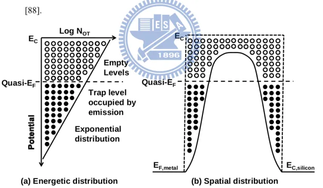
Fig. 2-8 Schematic trap level distribution at 0ok, in the oxide (a) energetically and (b)
spatially. Exponential trap distribution is assumed in (a). Trap levels filled with electrons are apparently separated from the unfilled trap levels on account of
zero Kelvin degree consideration. Solid and hollow circles correspond to the
trap sites with electrons and without electrons, respectively [90]. --- 27
Fig. 2-9 Gate current as a function of oxide trap density Not in arbitrary scale [93]. --- 28
Fig. 2-10 Four kinds of polarization mechanisms [96]. --- 28
Fig. 2-11 The relation of the response frequency and polarization mechanisms [97]. --- 29
Fig. 3-1 (a) The schematic layout of the La2O3 high-k MIM capacitors. (b) The cross-sectional structure along the A-A’ dashed line in the layout shown in (a). -- 41
Fig. 3-2 The main fabrication steps of the MIM capacitor with the La2O3 high-k dielectric and the process steps corresponding to their used photo masks. (a) Bottom electrode deposition and patterning. (b) ILD1 deposition and capacitor hole region opening. (c) High-k dielectric (HK) deposition and furnace annealing. (d) Top electrode deposition and patterning by using the lift-off technique. (e) ILD2 deposition and contact hole opening. (f) HK etching. And (g) Al deposition and patterning.--- 44
Fig. 3-3 The total injection charges density (Qinj) of MIM capacitor extracted from the area under the curve of the stress current density (Jstress) versus stressing time. --- 45
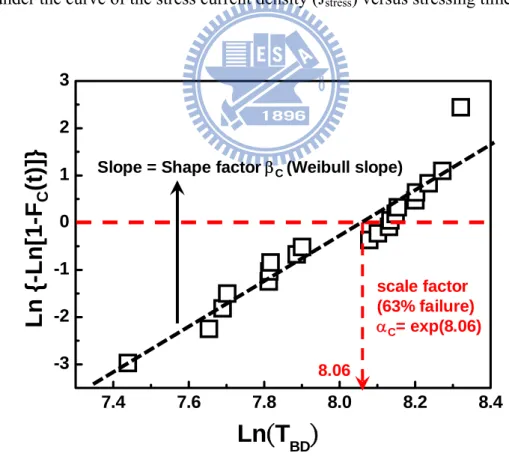
Fig. 3-4 The shape factor βC (Weibull slope) and the scale factor αC extracted from the TDDB plot. --- 45
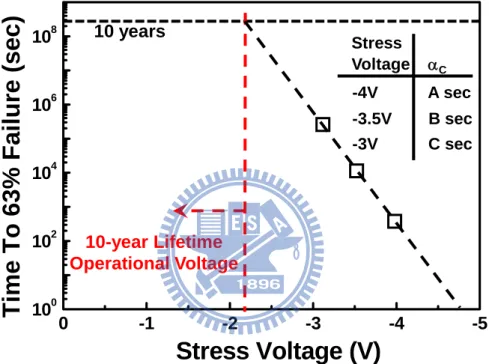
Fig. 3-5 The lifetime projection of MIM capacitors obtained from the failure plot with various stress voltages. --- 46
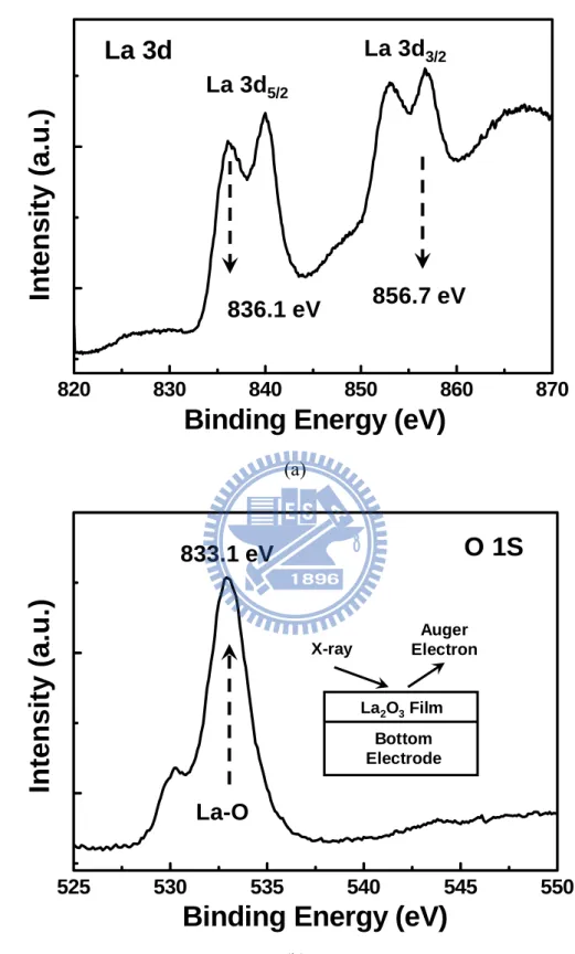
Fig. 4-1 The XPS spectra of the deposited La2O3 film. (a) The La 3d core level spectra, and (b) the O 1s core level spectra for the La2O3 film on bottom electrode.--- 68
Fig. 4-2 The C-V characteristic of the La2O3 MIM capacitor at 100 kHz and at 25ºC. The inset is the cross-sectional TEM image of the proposed La2O3 MIM capacitor. -- 69
Fig. 4-4 The J-V curve of the 10-nm La2O3 MIM capacitor measured at 25 °C. --- 70
Fig. 4-5 J-V curves of the La2O3 MIM capacitor in the case of top injection at
measurement temperatures in the range from 25 °C to 125 °C. --- 70
Fig. 4-6 The plot of ln(J/E) versus E1/2 in the high field region according the
Poole-Frenkel emission and the deduced static dielectric constant at various temperatures are also presented. --- 71
Fig. 4-7 The plot of the slope versus (qE/π)1/2 by various applied voltages fitting (a) from
25 °C to 75 °C, and (b) from 75 °C to 125 °C. --- 72
Fig. 4-8 Typical plot of lnJ versus E1/2 in the low field region according the Schottky
emission and the deduced static dielectric constant at various temperatures are also presented. --- 72
Fig. 4-9 The plot of ln(J/T2) versus q/kT in the applied voltage from −0.6 V to −1.6V.
The inset is the plot of the extracted slope versus E1/2 to obtain the extracted εr
value. --- 73
Fig. 4-10 C-V curves of the 10-nm La2O3 MIM capacitor measured under the frequencies
varied from 10 kHz to 500 kHz and at the temperature of 25 °C. --- 73
Fig. 4-11 (a) The VCC fitting curves and the extracted α values at the frequency ranges
from 10 kHz to 500 kHz at 25 °C in the case of top injection, and (b) the comparison in α between top and bottom injection condition at 25 °C. --- 74
Fig. 4-12 The extracted α values under various frequencies and different temperature
conditions of the La2O3 MIM capacitors in the case of top injection. --- 75
Fig. 4-13 The capacitance-temperature relationships at frequencies range from 10 kHz to
500 kHz for 10-nm La2O3 MIM capacitors. --- 75
Fig. 4-14 The normalized capacitance as a function of temperature and the corresponding
Fig. 4-15 The TCC values measured under zero bias, −1.5 V, and 1.5 V at frequencies
varied from 10 kHz to 500 kHz. --- 76
Fig. 4-16 The relationship between capacitance and operational frequency at the
temperature in the range from 25 °C to 125 °C. --- 77
Fig. 4-17 The normalized capacitance as a function of frequency and the corresponding
extracted FCC parameters at the temperature in the range from 25 °C to 125 °C. 77
Fig. 4-18 (a) The evolution of J-V curves of the La2O3 MIM capacitor stressed at −5 V in
the case of top injection, and (b) illustrates the absolute magnitude of [J(t) −J(t=0)] as a function of applied voltage with different stress time obtained from (a). --- 78
Fig. 4-19 The relative leakage variation ΔJ/J(t=0) measured at the applied voltage of −1 V
as a function of (a) stress time, and (b) injection charges (Qing) under t under the
stress voltage of −4.6 V, −4.8 V, and −5 V. --- 79
Fig. 4-20 Illustrates trap generation probability per injected charge (Pgen) under the stress
voltage of −4.6 V, −4.8 V, and −5 V as a function of stress time. --- 80
Fig. 4-21 The long-term evolution of ΔJ/J(t=0) at −1V with the increase in (a) stress time,
and (b) injection charges (Qinj) under the stress voltage of −4.6 V, −4.8 V, and −5
V. --- 81
Fig. 4-22 Relative-capacitance variation [C(t)-C(t=0)]/C(t=0) at 100 kHz as a function of
(a) stress time, and (b) injection charges (Qinj) at various CVS voltages from
−4.6 V to −5 V. --- 82
Fig. 4-23 (a) The time dependence of relative capacitance variation at various CVS
voltages from −4.2 to −4.6 V and the 10-year degradations. (b)The 10-year stability extraction of 10-nm La2O3 MIM capacitors estimated by the
Fig. 4-24 The relative quadratic voltage coefficient of capacitance α(t)/α(t=0) under CVS
from −4.6 V to −5 V as a function of (a) stress time, and (b) relative variation in dielectric loss D. --- 84
Fig. 4-25 The relative quadratic voltage coefficient of capacitance α(t)/α(t=0) under a
CVS voltage of −4.8 V with various measurement frequencies as a function of (a) stress time, and (b) relative variation in dielectric loss D. --- 85
Fig. 4-26 The relative temperature coefficient of capacitance TCC(t)/TCC(t=0) under
CVS from −3.8 V to −4.2 V as a function of (a) stress time, and (b) relative variation in dielectric loss D. --- 86
Fig. 4-27 The cumulative results of TZDB for the 10-nm La2O3 MIM capacitors at the
measurement temperature varied from 25 °C to 125 °C. --- 87
Fig. 4-28 (a) The Weibull distribution of TDDB as a function ln(TBD) and the extracted αc
and βc with a −4.2-V CVS at 75 °C. (b) The Weibull distribution of TDDB as a
function of TBD and the extracted αc and βc values under a CVS of −4.1 V to
−4.2 V at 75 °C. --- 88
Fig. 4-29 The 10-year lifetime projection to the normal operational voltage by
extrapolating all the αC data obtained from Fig. 4-28(b). --- 88
Fig. 4-30 (a) Time-dependent of Jstress under a −4.1-V CVS at 75 °C. (a) The Weibull plot
of time-dependent soft breakdown (SBD) and hard breakdown (HBD) under a −4.1-V CVS at 75 °C. --- 89
Fig. 5-1 The wear out to final breakdown evolution of the La2O3 MIM capacitors under
CHAPTER 1
I
NTRODUCTION
Recently, metal-insulator-metal (MIM) capacitors integrated into the backend metal interconnect level as passive components have been generated great interest for radio frequency (RF) and analog applications within Si integrated circuits (ICs) [1], [2]. For example, MIM capacitors are widely used for RF bypass and decoupling capacitors [3]-[5] or for digital-to-analog (D/A) and analog-to-digital (A/D) converters [6] due to their high conductive electrodes and low parasitic capacitance [7], [8]. Because the metal-oxide-semiconductor (MOS) capacitor usually consumes a large fraction of the whole chip area, the MIM capacitor with high capacitance density have been eagerly anticipated to reduce chip size and system cost [9]. However, since the leakage and reliability issues limit the aggressive thickness scaling, the higher capacitance density of MIM capacitors cannot be achieved by further thinning the conventional silicon dioxide (SiO2) or silicon nitride (SiN)
films [10]. Therefore, the only one choice is adopting high dielectric constant (high-k) materials as dielectrics of MIM capacitors.
In the last few years, many high-k dielectrics, such as Ta2O5 [11], HfO2 [12], Al2O3 [13],
TiO2 [14], various compound of these materials [15]-[17], and combinations of these
dielectrics as sandwich or laminate structures [18]-[20], have been investigated for MIM capacitors. Unfortunately, in spite of possessing higher capacitance density, many obvious drawbacks become the challenges for developing the high-k MIM capacitors, as described below. Fig. 1-1 shows that the trend of dielectric bandgap declines with the increase of dielectric constant [21]. Besides, the empirical data about the dielectric constant (k), the energy bandgap (Eg), and the conduction band offset with respect to the Si (ECB) of various
conduction band offset of high-k dielectric with respecting to the metal electrode result in larger leakage current and higher power dissipation, compared to conventional SiO2 MIM
capacitors. Secondly, it has been reported that the capacitance of the MIM capacitor with high-k dielectric would sensitively vary with the operational voltage, the temperature, and the frequency leading to distortion in analog signals for RF/analog applications [11]-[13], [15]-[20], which ultimately limit the performance of circuits. Although several studies have made efforts to discuss these phenomena [6], [23]-[25], the physical mechanisms of these influences on capacitance are still unclear. Accordingly, the large dependence of capacitance on voltage, temperature, and frequency is remaining a question for high-k MIM capacitors, and it is necessary to investigate and solve. Thirdly, earlier researches stated that the electric breakdown strength of MIM capacitors reduces sharply with the increase of dielectric constant [26], [27]. Besides, unlike the SiO2 which is an almost ideal insulating oxide, the
high-k dielectrics usually have high trap density in themselves and they have lots of interface states with electrode to cause the instability and unreliability of devices during operation [28]-[31]. Hence, from the view point of practical use, the electrical stress induced degradation and the breakdown strength of high-k MIM capacitors are serious concerns. However, a few researches have evaluated the wear-out behaviors and the statistical reliability results of high-k MIM capacitors, especially for high capacitance density (> 10 fF/μm2) MIM
capacitors. Therefore, the points mentioned above have to further study to improve the performance of high-k MIM capacitors.
According to the International Technology Roadmap for Semiconductor (ITRS) [32], as shown in Table 1-2, the RF MIM capacitors have to meet the following main demands: (1) high capacitance density (> 5 fF/μm2), (2) low leakage current (< 10-8 A/cm2), (3) high breakdown electric field (holding at least a voltage bias of 5 V), (4) very small voltage linearity (< 100 ppm/V2), and (5) low dielectric loss [tanδ < 0.05, i.e., Q factor (=1/ tanδ) >20]. Moreover, since the high-k MIM capacitor for RF/analog applications is located in the
interconnection levels and above the active integrated circuit layers, the maximum fabrication process temperature is limited to 400 °C to fulfill the low thermal budget requirement of the very large scale integrated circuits (VLSI) backend process.
To replace conventional SiO2 and SiN dielectric materials, a new suitable dielectric can
be selected in terms of energy bandgap and dielectric constant, which are usually trade-off for high-k materials, as depicted in Fig. 1-1 and Table 1-2. A considerable number of studies have been conducted on hafnium (Hf) or zirconium (Zr) based oxide, but Hf or Zr based oxide does not meet the requirement of next generation where the equivalent oxide thickness (EOT) of dielectric needs less than 1 nm. Therefore, the other alternative dielectrics, rear-earth metal oxides (REOs), are being focused. And, the energy bandgaps of REOs are also revealed in Fig. 1-2 [33].
Among the REOs, lanthanum oxide (La2O3), or named as Lanthana, has the highest
potential to achieve less than 1-nm equivalent oxide thickness (EOT) [34]. In addition, various superior characteristics of thin La2O3 film have been reported, including a large
bandgap (> 5 eV) [34], [35], a relatively high dielectric constant (20-30) [34], [36], [37], a high breakdown electric field [27], [38], a low interface state density [34], [36], a low leakage current with small EOT [34], and a good oxide reliability [39]. As a result, the La-based oxide is the most promising candidate for the next technology node. However, up to present, the investigation on La2O3 MIM capacitors is very little [3], [40], and the characteristics of La2O3
MIM capacitors, such as stress behaviors, breakdown, and reliability issues, are unclear and essential to demonstrate. Consequently, we adopt the La2O3 as the dielectric of MIM
capacitors to study in detail in this work, and we could establish a base to develop and really carry out the high performance La-based high-k MIM capacitors for RF/analog applications in the future.
The objective of this thesis is to achieve a fundamental understanding of the working principles and the implementation issues of the La2O3 high-k MIM capacitors for VLSI
backend applications. The innovation and major topics of this research are addressed as following. For one thing, although there are several reports on the electrical properties of La2O3 thin films on the basis of MOS structure [37], [41], [42], the conduction mechanisms of
the lanthanum oxide are not fully understood, and the conduction behaviors of La2O3 high-k
MIM capacitors have not been evaluated yet. Thus, we measure the leakage current of 10-nm La2O3 MIM capacitors and analysis the conduction mechanisms at various temperatures.
What is more, the capacitance of high-k MIM capacitors sensitively varies with applied voltage, temperature, and frequency, which could be depicted by quadratic voltage coefficient of capacitance (α), temperature coefficient of capacitance (TCC), and frequency coefficient of capacitance (FCC). However, the opinions about origins of these phenomena are widely divided and unclear. Therefore, we study it in detail and discuss physical mechanisms, according to the high-k dielectric behaviors, for instance, dielectric polarization and relaxation. In terms of factors that induce α, TCC, and FCC, we suggest the possible solutions to improve the analog distortion events for high-k La2O3 MIM capacitors.
Additionally, despite the trap-rich nature for high-k dielectrics would cause the instability and unreliability of devices during operation, the study on degradation and reliability characteristics for La2O3 MIM capacitors under electrical stress is still an
undeveloped field. As a result, we demonstrate the long-term evolution of the leakage current and the capacitance for 10-nm La2O3 MIM capacitors under constant voltage stress (CVS).
We also observe the variation in α and TCC under CVS, which further clarify the physical origins of it. Finally, we inquire the time-dependent dielectric breakdown (TDDB) and the time-zero dielectric breakdown (TZDB) of La2O3 MIM capacitors to verify the lifetime and
0 5 10 15 20 25 30 35 3 4 5 6 7 8 9 10
Energy Bandgap (eV)
Dielectric Constant
SiO
2Si
3N
4Al
2O
3MgO
CaO
ZrSiO
4HfSiO
4Y
2O
3ZrO
2HfO
2La
2O
3Ta
2O
5BaO
Pr
2O
3Fig. 1-1. The bandgap as a function of dielectric constant for various candidate oxides [21].
1 2 3 4 5 6 7
Ene
rgy
B
andga
p (e
V)
Lanthanide Oxides
La
2O
3Ce
2O
3Pr
2O
3Nd
2O
3Sm
2O
3Gd
2O
3Eu
2O
3Tb
2O
3Dy
2O
3Ho
2O
3Er
2O
3Yb
2O
3Tm
2O
3Lu
2O
3Table. 1-1. The empirical data about dielectric constant, energy bandgap, and conduction band
offset with respect to the Si of various high-k dielectrics [22].
Dielectric Dielectric Constant Bandgap (eV) Conduction band offset SiO2 3.9 9 3.5 Si3N4 7 5.3 2.4 Al2O3 ~10 8.8 2.8 Ta2O5 25 4.4 0.36 La2O3 ~21 6 2.3 Gd2O3 ~12 --- ---Y2O3 ~15 6 2.3 HfO2 ~20 6 1.5 ZrO2 ~23 5.8 1.4 SrTiO3 --- 3.3 ~0.1
Table. 1-2. Requirements for RF MIM capacitors according to ITRS [32].
4 5 5 7 10 10 2008 2010 2012 2014 2016 2018 <100 <100 <100 <100 <100 <100 <10-8 <10-8 <10-8 <10-8 <10-8 <10-8 0.5 0.4 0.4 0.3 0.2 0.2 >50 >50 >50 >50 >50 >50 Year of Production C (fF/μm2) VCC (ppm/V2) Leakage (A/cm2) Matching (%-μm) Q (5GHz for 1pF) Metal-Insulator-Metal Capacitor
CHAPTER 2
G
ENERAL
B
ACKGROUNDS AND
L
ITERATURES
R
EVIEW
In this chapter, we first give a introduction on high-k dielectric conduction mechanisms, including Schottky emission (SE), Poole-Frenkel (PF) emission, space-charge-limited current (SCLC), and the conductions related to high trap density insulator. Secondly, section 2.2 describes dielectric behaviors comprise dielectric polarization and dielectric relaxation in high-k MIM capacitors. Subsequently, section 2.3 reviews several literatures regarding stress induced variations in properties of MIM capacitors. Finally, section 2.4 states a concise history on reliability improvement of silicon-based devices and then indicates the most interesting reliability issues on MIM capacitors for RF/analog application.
2.1 C
ONDUCTIONM
ECHANISMS INH
IGH-
KD
IELECTRICSTwo types of electrons exist and transport in the insulator of MIM capacitor: intrinsic electrons and extrinsic electrons [43]. Intrinsic electrons natively exist in insulator, and extrinsic electrons inject from the nearby electrode to insulator. Because the carrier density of intrinsic electrons inside the insulator is low, the conduction mechanism of intrinsic electrons is like the ohmic type with a large resistivity. However, there are two possible cases in extrinsic electrons. First, the current is only limited by the bulk of insulator due to the unlimited electron sources of the electrodes. Second, if the electrodes restrict the carrier injection, the injection electrons would travel free inside the insulator. According to these two viewpoints, the conduction mechanism in insulator could be classified into bulk-limited and electrode-limited (bulk-free) ones for extrinsic electrons. Tables 2.1 and 2.2 summarize
various bulk-limited and electrode-limited conduction mechanisms, respectively, which are used to investigate the leakage conduction [39], [43]-[53] of our MIM capacitor in this work. Following, the conduction mechanisms of Schottky emission (SE), Poole-Frenkel (PF) emission, space-charge-limited current (SCLC), and some other high trap density related conductions are further described in below subsection.
2.1-1 Schottky Emission
The Schottky effect describes the image-force-induced barrier lowering for charge carrier emission [39]. Fig. 2-1 shows the energy-band diagram between a metal surface and a vacuum level while electron movies close to electrode. The maximum barrier height of vacuum level would be reduced due to the image force at interface of metal Fermi level and vacuum level. The Schottky emission (SE) is analogous to thermionic emission except for the barrier height lowing due to the external field applying. However, this barrier height lowing could help the thermally activated carriers emit from the metal electrode, called Schottky emission. Metal-vacuum system, as shown in Fig. 2-1, is also equivalent to metal-insulator system, except for the dielectric constant of the vacuum part and the insulator part. The main feature of SE is Schottky barrier lowering (or image force lowering) [39].
4 ΔφB = qE
πε (2-1)
Here, permittivity ε should be replaced by an appropriate permittivity characterized by the inserted medium. The tunneling current could be written by [43], [54]-[56]
* 3 4 [ ( ) ( )] [ ( ) ] m m E n n t x x E E m q J f E f E V D E dE dE h π ∞ =
∫
− + ×∫
• • . (2-2)Here, h is Planck constant, f is Fermi distribution function, Dt is tunneling probability, Em is
barrier height, and V is applied voltage. Since carrier emission occurs at much higher energy level than Fermi level of the injecting electrode, the tunneling probability (Dt) could be
regarded as 1. Then, the integration in Eq. (2-2) yields * 2 3 4 ( ) exp( m F)[1 exp( )] B B B E E m q V J k T h k T π − = − − k T − . (2-3)
Here, the Schottky barrier lowering modified from Eq. (2-1) could be written as
0 0 0 4 − = − Δ = − m F B i qE E E φ φ φ πε ε . (2-4)
Therefore, the Eq. 2-3 under V >> kBT condition could be simplified as B
* 1 2 2 3 4 ( ) exp( B ) exp( S ) B B B m q J k T h k T k β φ π = − E T (2-5) , where 12 0 ( 4 S i q β πε ε
= ) . Eq. (2-5) is also called Richardson-Schottky equation [72].
The Schottky current is thermally activated process with the activation energy characterized by Eq. (2-4). The activation energy could be modulated by the applied bias with Schottky barrier height lowering effect. One notices that the barrier deformation decreases as the dielectric constant increases, indicating that SE in high-k oxide films seems to be less probable than that in conventional SiO2 film due to higher lower dielectric constant and much
defect density in their self.
2.1-2 Poole-Frenkel Emission
The potential barrier lowering also affects the Poole-Frenkel (PF) emission current while applying an external field. However, the SE is associated with the insulator barrier near to the injection side of the electrode, but the PF effect is associated with barrier at the trap site in the bulk of insulator film. Thus, neutral donor traps, which are neutral when filled but positive when empty, do not experience the PF effect owing to the absence of the Coulomb potential. Fig. 2-2 shows the thermionic emission of trapped carriers occurs at the trap site in the bulk film. Internal thermionic emission is called PF emission, while external one is called Schottky emission. The other way for electron emission is hopping process, which is a kind of tunneling process in a short range. The difference between the SE emission and the PF
emission are summarized in Table 2.3. Here, it should be noted that PF emission is closely related to the oxide film thickness but Schottky emission is not, as far as the equal electric field on dielectric is concerned. Fig. 2-3 illustrates that the restoring force in both Schottky and PF effects comes from Coulomb interaction between the escaping electron and the image charge (positive) [57]. The restoring force due to electrostatic potential makes electron move back to its equilibrium position. Although the restoring force is the same for the escaping electron and the image charge, these charges differ in the positive image charge fixed for PF barriers but mobile fixed with SE. It results in a barrier lowering twice as great for the PF effect, as shown in Eqs. (2-7) and (2-8).
3 1 1 2 2 0 ( ) PF PF q E E φ β πεε Δ = = (2-7) 3 1 1 2 2 0 ( ) 4 S S q E E φ β πεε Δ = = (2-8)
In that the electrons have enough energy to go over the energy barrier and travel in the conduction band with a mobility μ dependent on the scattering with the lattice, the general expression of the bulk current is expressed by [43]
( )
J =qn x Eμ . (2-9)
The concentration of free carriers in the insulator is
exp[ ( )] C C q n N E E kT = − − F . (2-10)
Since EC−EF is equal to the effective trap barrier height, including the barrier lowering effect
described by Eq. (2-7), the effective barrier height and the current governed by the PF emission are written by Eqs. (2-11) and (2-12), respectively.
1 2 C F S PF S PF E −E =φ − Δφ =φ −β E (2-11) 1 2 exp( S ) exp( PF ) C B q J qN E E kT k T φ β μ = − (2-12)
On the other hand, the PF emission will lower the barrier height of dielectric film when the dropping field is higher than the critical field [58] as
2 ( i ) crit PF E φ β = (2-13)
, where φi is the trap barrier height at zero oxide field. At electric field higher than Ecrit., the
emission process, instead of bulk-process, begins to play a dominant role.
2.1-3 Space-Charged-Limited Current
Space-charge-limited current (SCLC) model has been developed and used continuously over four decades. Until now numerous attempts have been reported to interpret the current behavior of thin films within the frame of SCLC. Such films are porous SiO2 [59]-[61], TiO2
[62], organic materials [63], porous silicon [64], [65], SiO2/Nitride [66], Si3N4 [67], [68],
SrTiO3 [69]-[72], Ta2O5 [59], [73], Al2O3 [74]-[76], Nb2O5 [77], and Nd2O3 [78], Gd-In-oxide
[79], Dy2O3 [80], [81], and La2O3 [82] in rare-earth metal oxides.
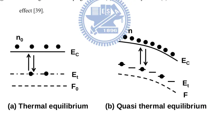
Fig. 2-4 shows the thermal equilibrium and the quasi-thermal equilibrium (i.e., steady-state) of electrons in the conduction band and in the trap levels of the dielectric film, respectively [83]. Electron carrier concentrations for both cases are related to electrons in trap levels. If the leakage current through the dielectric is bulk-limited, the magnitude of the current is determined by the electrons in the conduction band. The concentrations of electron carriers at the thermal and quasi-thermal equilibrium in the conduction band are strongly affected by the trap level density trap levels, and injection electrons to the trap levels. It implies that, with the help of equilibrium approximation, the leakage current could be described as electrons in energy and space, causing accumulation of charges due to injected electrons, so called the space charges.
The space-charge-limited current at room temperature or below is efficient on the electrical properties of dielectric insulators because they normally have a low density of free carriers, and the charge unbalance could be easily produced by the external applied voltage. The character and the magnitude of space-charge-limited effect are largely determined by the
presence of localized states which could trap and store charges in equilibrium with the free carriers. When the charges effectively inject from the conduction (or valence) band into insulator, the net transport is limited by the actual transport, drift and diffusion, of charges in the bend of the insulator. Regarding the electron injection into the oxide film, it seems difficult for electrons to jump into the conduction band by thermal transition or tunneling process. However, if the dielectric has a large trap density or a large tail density of state (DOS) near the electrode, as shown in Fig. 2-5, electrons are able to excite into the conduction band with a small activation energy [84]-[86].
Fig. 2-6 shows the oxide band structure distorted by the injection electrons. In order to satisfy the thermal equilibrium, electrons inject from the cathode into the insulator, resulting in a negative space-charge density adjacent to the cathode. Because an equal amount of positive charges remain on the cathode, the charges distribution consists of positive charge sheet near a region with negative space charges. The same condition is also on the anode side. As the voltage bias increases, the net positive charges on the cathode would be increased and that on the cathode would be decreased. Total charge Q in the insulator could be expressed by the sum of the cathode positive charge Q1 and the anode positive charge Q2 [87] as
1 2 0 ( ) ( ) m m s Q Q Q λ x dx x dx λ ρ ρ = + =
∫
+∫
. (2-14)The positive charges on either contact are neutralized by an equal amount of negative charges contained between the contact and the plane at x=λm. Since the internal field caused by Q1 and
Q2 is zero at x=λm, the net field there must be zero. For this reason, the place at x=λm is
termed the virtual cathode. Eventually, when Q1=0, the virtual cathode coincides with the
physical cathode-insulator interface. Under this condition, the anode region extends throughout the whole of the insulator, and the ohmic contact no longer exists at the cathode-insulator interface. Thus, due to further increasing voltage bias, the conduction process is no longer space-charge limitation, but it belongs to emission limitation.
Space charges have an effect to distort the oxide dielectric band shape. In electron carriers case, the tunneling distance and the barrier height are increased by accumulation space charges so that the tunneling current is depressed [45]. The space-charge-limited flow is known to be effective at room temperature or below, since the low density of free carriers easily cause charge unbalance [45]. This is also valid on high-k materials with a considerable charge trap density at high temperature. Fig. 2-7 shows that the typical J-V behavior obeys the SCLC theory with the combination of exponential and the localized trap level distributions. In the logarithmic scale of J-V curve as shown in Fig. 2-7 (a), it could be easily found a linear relationship according to the SCLC theory. On the other hand, in the semi-logarithmic scale as shown in Fig. 2-7(b), it is difficult to realize the exacted J-V relationship.
The space-charge-limited current with localized trap levels in the oxide band is given by
2 0 3 9 8 ox V J L ε ε μ = . (2-15)
Here, ε0 and εox are dielectric constants of vacuum and oxide film, respectively. μ is carrier
mobility, V is applied voltage, and L is film thickness. The mobility μ is often found to be strong dependence on electric field, particularly in the high field region [88]. The space-charge-limited current with exponential trap levels is given by
( 1) (1 ) ( 1) (2 1) 2 1 [ ] ( ) (1 ) 1 l l l l c l t l l V J N q N l l L ε μ − + + + + = + + . (2-16)
Here, Nc is density of states at conduction band, q is electronic charge, and Nt is total trap
density. l=Tt/T, where Tt is described as trap level distribution and T is absolute temperature.
As seen in Fig. 2-6, the accumulation charges near to the cathode leads to virtual cathode in the oxide film. This means that the carrier transport is caused by the drift field between the virtual cathode and anode, with a continuous supply of charges from the accumulation region between the virtual cathode and the real cathode. So, we could expect that the electric field near the cathode is small and that in the drift current flow region is large. This point can be realized by the oxide electric field as a function of position, which is given by
1 2 1 ( ) ( )( ) 1 l l l x E x l L + + = + V L. (2-17)
The effective field in oxide film near the cathode is nearly zero and it is higher than the applied field. This higher electric field may result in the larger current, especially in the thin dielectric. Fig. 2-8 shows the typical trap levels with the exponential energy distribution and with the maximum trap density distribution. As regard to the spatial distribution of trap levels, uniform or non-uniform type of distribution does not alter the results of J-V relation, because the spatial trap distribution is only affected by the film thickness [46], [89]. In addition, the energetic trap distribution in the energy bandgap of oxide determines the J-V relation, such as J~V, J~V2, or J~V(n+1). The oxide film thickness in SCLC with a uniform trap distribution is equal to the physical film thickness (d), while the film thickness with spatially distributed traps is effective film thickness (deff). The effective film thickness describes the trap
distribution inside the film. The J-V relation remains unchanged and it is independent of how the trap is distributed spatially.
2.1-4 High Trap Density Related Conduction
Excepting for the PF emission and SCLC, there are also several conduction mechanisms related with high trap density in dielectric, such as Poole conduction, trap-assisted tunneling (TAT), junction-like conduction, and variable range hopping (VRH), as noted in Tables 2.1 and 2.2. And, we briefly describe them as following.
Poole conduction and P-F conduction assume paired trap sites and isolated trap sites, respectively [90], depending on the oxide trap density. The transition between two models has been reported in [91]. As the applied field becomes lower, the current density following P-F conduction could be described by Poole conduction because the barrier height reduction by the electric field becomes smaller, and then the trap level is comparable to that of the Poole [91]. In Poole conduction, traps are enough close to perturb the Coulombic potential of the
neighbor trap, so that the decrease of the barrier height between two traps is determined by distance between traps and applied field but not by Coulombic field. It leads to leakage current independent of the dielectric constant of the insulator.
Variable range hopping (VRH) conduction involves thermally activated hopping conduction in localized electronic states near the Fermi energy. VRH conduction dominates the conduction mechanism at low applied voltage and high temperature [92]. Besides, TAT conduction requires shallow and/or deep trap levels and it usually occurs at the oxide field greater than 4 MV/cm [93], [94]. Fleming et al. suggested that leakage current could flow through the defect band formed by localized large trap levels, and then its behavior is similar to the junction-like conduction due to the difference in energy level between the defect band and the Fermi level at both electrodes [95].
As regard to the relation between oxide trap density and leakage current, the traps enhance the leakage current for the case of Poole, VRH, TAT, and junction-like conductions, while they hinder it in SCLC case. This is the uniqueness of SCLC contrast to the others. Fig. 2-9 conceptually illustrates the relationship between the leakage current and the trap density of the dielectric film. If the gate current is explained by the SCLC theory, the gate current could be reduced by increasing the dielectric trap density.
2.2 D
IELECTRICP
OLARIZATION ANDR
ELAXATION OFH
IGH-
KMIM
C
APACITORS2.2-1 Dielectric Polarization
In an MIM capacitor system composed of two parallel metallic plates with an insulator thickness d (in meter, m), the capacitance CMIM (in farad, F) is calculated by using
MIM Q S C V d ε× = = (2-18)
, where V (in volt) is the applied voltage of the capacitor, Q (coulomb, C) is the amount of storage charges of the capacitor, ε (in F/m) is the permittivity of the insulator, and S (in m2) is the area of the plate. The capacitance is proportional to the permittivity which signifies the charge storage capability of the capacitor, and the large permittivity of the high-k dielectric contributes from the lattice structure and the polarizability under the external bias. The lattice structure of the dielectric determined by the crystal phase has been formed as the dielectric film deposited or grown during the fabrication process. Therefore, the changes in permittivity of high-k MIM capacitor during measurement could be contributed to the changes in polarization behaviors.
In general, the total polarizability of a dielectric could be divided into four kinds of possible compositions, as sketched in Fig. 2-10 and denoted below [96].
(1) The electronic polarizability, pe, is caused by the slight displacement of the negatively
charged electron cloud in an atom relative to the positively charged nucleus. Electronic polarizability occurs in all solids and in some, such as diamond, and it is the only contributor to the dielectric constant since ionic, dipolar, and space charge polarizabilities are absent.
(2) The ionic polarizability, pi, arises from a slight relative displacement or a separation of
anions and cautions in a solid.
(3) The dipolar polarizability, pd, arises in materials, such as HCl and H2O, which contain
permanent electric dipoles or are induced by the defects and polar molecules in the dielectric. These dipoles may change their orientation and they tend to align themselves with an applied electric field. The effect of dipolar polarizability has large temperature dependence since the dipoles may be “frozen” at low temperature.
(4) The space charge polarizability, ps, occurs in unperfected dielectric with a long range
charge migration.
expresses as follows:
e i d s
p= p +p +p + p (2-19)
2.2-2 Dielectric Relaxation
As described above, the total polarizability in dielectric composed of electronic polarizability, ionic polarizability, dipolar polarizability, and space charge polarizability can contribute to the permittivity. However, as the polarity of external force changes, all the polarization species, like electrons, ions, dipoles, and space charges, need a period of time to displace from the original site or rotate from the earlier orientation to the new equilibrium state, resulting in the other polarization status. This lag response process of the dielectric is the dielectric relaxation, and the period of time when the polarization specie needs to follow the alternating force is the relaxation time. Moreover, four kinds of polarization species have various response times, and Fig. 2-11 reveals the relation between the polarization mechanism and the alternating frequency of external force that the polarization can follow [97]. We can recognize from this diagram that the space charges have the longest relaxation time than any other polarization species, and their polarized phenomenon could be neglected as the alternating frequency of external force is higher than 1 MHz. But, the electrons can rapidly response the changes of external force to result in the shortest relaxation time, and hence such rapidly response of electrons can contribute to the polarization even at very high frequency. In a trap-rich dielectric, such as many high-k materials, the dipolar relaxation and the space charge relaxation are emphasized at our testing frequencies in the range from 10 kHz to 500 kHz. Thus, we give a brief description about these two types relaxation behaviors as following.
Space charges in dielectric of the high-k MIM capacitor are made of free carriers that inject from the biased electrode, and then they become the excess mobile charges moving in the dielectric film [98]. The excess mobile charge in the insulator is expected to follow the
alternating signal with a relaxation time τs depending on the mobility μ, the mobile charge
concentration n(E), and the permittivity ε. According to Coelho [99], the complex permittivity ε* is given by * ' '' 1 tanh( ) s s i j A i A ωτ ε ε ε ε ωτ + = − = × + (2-20)
, where ε’ is the real part of the complex permittivity and ε’’ is the imaginary part of the complex permittivity. And, A is given by
1 2 s E s i d A D ωτ τ + = × (2-21)
, where d is the thickness of the dielectric, ω is angular frequency, and DE is the diffusion
coefficient according to Einstein’s law (DE=μkT/e). The relaxation time (τs) is given by
( ) s en E ε τ μ = . (2-22)
Here, n(E) is mobile charge concentration dependant on the electric field E. A higher relaxation time means the mobile charges are more difficult to follow the alternating signals. The frequencies that space charge can follow are low, we would observe the tail of the space charge relaxation at the test frequencies (10 kHz to 500 kHz). If the conduction of the MIM capacitor is given by Schottky effect, the n(E) could be expressed as the following formula
1 2 0 ( ) exp( ) exp( ) 2 S B B B e n E n E k T k T β φ = − (2-23)
, where n0 is uniform concentration of mobile charges without any applied voltage.
Accordingly, the amount of excess mobile charges in the insulator could be affected by the electric field, the temperature, and the barrier height at the metal/dielectric interface.
The dipole relaxation effect can be observed even at infrared frequency while the free carrier effects become negligible. The dipolar relaxation time (τd) shows a wide distribution
range of 10-10 sec to 103 sec, which results in a broad frequency range where the dipole can contribute to the dielectric relaxation. It has been reported that the defect dipole relaxation
dominates the lower frequency part or the longer relaxation time region of the total dipolar relaxation behaviors [100]. Besides, as the temperature increases, the τd decreases to manifest
a faster response for alternating signals.
2.3 S
TRESSB
EHAVIORS OFMIM
C
APACITORSIn terms of the precision performance of long-term use, it is a key issue that the stability of MIM capacitors under electrical stress. C. Besset et al. [101] first depicted the variation of the SiO2 MIM capacitance under electrical stress, and they also observed that the
relative-capacitance variation is dependent on the injection charges but independent of the stress current. Additionally, it was also found that the capacitance-voltage curve shifts toward the negative voltage side and the capacitance density significantly increases. And, it concluded that both phenomena on the C-V shift and the capacitance increase are strongly correlated and they had the same origin of the trapped charges, which could generate new dipoles in the dielectric and modulate the dielectric permittivity.
C. C. Hung et al. [102] investigated the degradation of SiO2 MIM capacitors under a
wide voltage range of stress conditions. It was found that the capacitance is gradually degraded during stress, but the degradation behavior strongly depends on the stress-current density. At high stress voltage level, the capacitance is increased logarithmically as the injection charges increase until the dielectric breakdown occurs. At lower voltage stress conditions, the degradation rate is proportional to the stress current and it is reversal after a certain period of time. The reversal phenomenon of the degradation rate begins in earlier at higher temperature. Initially, the oxide-trapped charges would increase the local permittivity of dielectric, thus leading to the capacitance increasing. On the other hand, a reversal in the degradation, after stressing for a certain period of time, may arise from a growth in the interlayer between the metal electrode and the dielectric.
C. Zhu et al. [103] and S. J. Ding et al. [104] demonstrated the stress induced leakage current and the stressed induced variation in voltage coefficient of capacitance (VCC) of high-k HfO2 and HfO2-Al2O3 MIM capacitors, respectively. It was argued that carrier
mobility could be modulated and become smaller by the stress generated traps, and further lead to a higher relaxation time and a smaller VCC. Later, C.-H. Cheng et al. [105] demonstrated the effects of the constant voltage stress (CVS) on the VCC, the leakage current, and the temperature coefficient of capacitance (TCC) of HfTiO MIM capacitors. They suggested that the elevated barrier height of the dielectric caused by the trapped electrons might suppress the leakage current under CVS condition. On the other hand, the stress induced variations in both VCC and TCC could be attributed to the electron-trap generation and/or ion displacement in dielectric. They also pointed out employing the metal electrode with higher workfunction could reduce these variations during stressing.
K. Takeda et al. [29] discussed the stress behaviors of high-k HfAlO MIM capacitors. In this research, it was discovered that the relative dielectric constant (k), the dielectric loss (D), the temperature coefficient of capacitance (TCC), and the frequency coefficient of capacitance (FCC), would gradually increase with the voltage stress time while the VCC decreases. It was also found that nearly linear relationships existed between k and D, between TCC and D, and between FCC and D are increased. These results indicated that the increases in k-value, in FCC, and in TCC during CVS conditions, are basically explained by the increase in D. Therefore, it is suggested that the voltage stress would cause the increase of dielectric-loss, and then increases k, FCC, and TCC. Increase in stress-time dependence of dielectric-loss was well described by power dependence, and that is, the power exponent of the dependence linearly increases with stress voltage. The power exponent could be lowered by increasing the aluminum concentration in HfAlO dielectric. This indicates that adding aluminum into the HfAlO dielectric can improve the characteristic stabilities of a MIM capacitor under voltage stress.
Former two studies imply that the high-k dielectrics have more obvious charge-trapping properties so that their stress induced degradation may be an issue on high-precision analog applications. However, the correlation between the injection charges and the capacitance variation of high-k MIM capacitor due to the electrical stress has not been well characterized. Besides, the relationship between VCC and D of high-k MIM capacitor under electrical stress still remains a question and needs to be clarified. Moreover, it is well-known that the high-k MIM capacitor has distinct conduction mechanisms under various bias conditions, which leads to diverse stress effects on leakage current. Therefore, the stress induced changes in leakage current in various bias ranges should be separately discussed.
2.4 R
ELIABILITYC
HARACTERISTICS OFMIM
C
APACITORS2.4-1 A Brief History on Reliability Improvement of Silicon-Related Device
Prior to 1985, the reliability improvements on silicon devices had already begun, and those efforts had already passed through two eras [106]. In the first era of the improvement of silicon reliability, from 1975 to 1980, the introduction of new VLSI materials was at the forefront. Everyone learned about material properties, such as Si, Al, and SiO2, and their
various interactions. In the second era, from 1980 to 1985, the major reliability problems for silicon technologies were identified: mobile ions, electro-migration, stress migration, time-dependent dielectric breakdown (TDDB), cracked die, broken bond wires, purple plague, and soft errors.
In the third era, from 1985 to 1990, the reliability physics was the focus on the silicon folks. The researchers developed various degradation models for the previously identified mechanisms and they also derived acceleration factors for the special environmental stresses of temperature cycling and corrosion. In the fourth era, from 1990 to 1995, the silicon folks adopted a new phrase, building-in reliability. It was a period of reliability engineering
emphasized on the wafer-level reliability. In the fifth era, from 1995 to 2000, the silicon folks complete their 20-year cycle by merging the metrics of reliability and quality with focus on a major defect-reduction effort. From 2000 to 2005, the silicon folks restart their cycle by reverting back to the first era, with the introduction of new materials in ULSI technology. The main work is on new copper metallization, low-k interlayer dielectrics, high-k gate dielectrics, new metal gate materials, and getting feature smaller than 100 nm.
2.4-2 Reliability Issues on MIM Capacitors
In the case of MIM capacitors, the ultimate breakdown strength of a dielectric material and their time-dependent dielectric breakdown (TDDB) characteristics have been attracted great reliability interest [107]. During electrical breakdown measurement, the ramping voltage (electrical field) is used to record an abrupt rise in leakage current through the dielectric of MIM capacitor. A rapid rise in current density could result in the severe localized joule-heating in the dielectric, the localized melting of the dielectric, and the melt-filament formation to short the dielectric between two electrodes.
TDDB properties depend on the intrinsic dielectric materials, the processing method, and the electrode materials. The MIM capacitor with thin dielectric film usually exhibits higher failure rate, thus it is a permanent challenge to improve of its TDDB properties. TDDB measurements are normally done by recording the times-to-failure when a collection of identically processed capacitors are stored under a constant electric field which is less than breakdown strength of the dielectric. The time-to-failure statistics are assumed to follow a Weibull distribution with appropriate “Weibull area scaling” for capacitors that differ only by their area [108]. The time-dependence of the TDDB process is derived from the fact that a critical amount of dielectric damage must be accumulated before the electrical breakdown and the thermal breakdown occur. From a microscopic point of view of the TDDB process, molecular bonds tend to break with time during TDDB testing, eventually reaching a
localized density of broken bonds sufficiently high to cause a conductive percolation-path to be formed between two electrodes. These conductive paths can result in electrical/thermal-breakdown of the dielectric.
Since high-k materials are aggressively developed to replace SiO2 as dielectrics film of
MIM capacitors, it is important to know whether high-k dielectrics provide superior reliability. In recent years, a number of studies have demonstrated the reliability characteristics of backend high-k MIM capacitors [29], [109]-[115]. However, most of them focus on the silicon nitride (SiNx) MIM capacitors [109]-[112], and other minorities investigate the reliability issues of Ta2O5, Nb2O5, Hf-based, and Zr-based MIM capacitors [29], [113]-[115].
As regard to La-based high-k MIM capacitors, there is no empirical research of statistical TDDB properties up to this point.
Δφ
Bφ
BΦ
m−χ
E
FMetal
x
mx
0qE
Xψ(x)
0
Conduction band edge (E=0)
Image potential
Conduction band
edge (E>0)
x
Fig. 2-1. Energy-band diagram between a metal surface and a vacuum. Conduction band edge
means the vacuum energy level which is zero in electron energy. x0 is introduced due
to the singular point of image potential at x=0 [39].
Trap site 1
x
0Φ
mΦ
m(x)
Trap site 2
Energy
x
Thermionic
conduction (P-F)
ΔΦ
PF=
β
PFE
OX1/2z z Image charge Escaping electron Electrode
(a) Schottky effect
Trap charge
Escaping electron z
(b) Poole Frenkel effect
Fig. 2-3. Restoring force on escaping electron. (a) The Schottky effect. (b) The Poole-Frenkel
effect [39].
E
CE
tF
0n
0(a) Thermal equilibrium
E
CE
tF
n
(b) Quasi thermal equilibrium
Fig. 2-4. Thermal and quasi-thermal equilibrium (steady-state) of electrons in conductionband Ec and trap level Et. F denotes quasi-Fermi level and the subscript 0 means the
thermal equilibrium [83]. The equilibrium states can be achieved by low injection and low internal emission.
![Fig. 1-1. The bandgap as a function of dielectric constant for various candidate oxides [21]](https://thumb-ap.123doks.com/thumbv2/9libinfo/8466762.183377/21.892.184.692.141.532/fig-bandgap-function-dielectric-constant-various-candidate-oxides.webp)
![Fig. 2-5. Mobility of electrons as a function of energy showing mobility gap (amorphous stste) [84]-[86]](https://thumb-ap.123doks.com/thumbv2/9libinfo/8466762.183377/42.892.213.692.118.414/mobility-electrons-function-energy-showing-mobility-amorphous-stste.webp)
![Fig. 2-9. Gate current as a function of oxide trap density N ot in arbitrary scale [93]](https://thumb-ap.123doks.com/thumbv2/9libinfo/8466762.183377/44.892.220.690.156.447/fig-gate-current-function-oxide-density-arbitrary-scale.webp)
![Fig. 2-11. The relation of the response frequency and polarization mechanisms [97]. Table 2-1](https://thumb-ap.123doks.com/thumbv2/9libinfo/8466762.183377/45.892.211.689.119.420/fig-relation-response-frequency-polarization-mechanisms-table.webp)
![Table 2-2. Theoretical expressions of the electrode-limited conduction processes in oxides [46], [48]-[51]](https://thumb-ap.123doks.com/thumbv2/9libinfo/8466762.183377/46.892.115.774.190.701/table-theoretical-expressions-electrode-limited-conduction-processes-oxides.webp)