應用於多頻帶正交分頻多工超寬頻系統之全積體化低功率快速鎖定整數型頻率合成器
99
0
0
全文
(2) 應用於多頻帶正交分頻多工超寬頻系統之全積體化 低功率快速鎖定整數型頻率合成器 A Fully Integrated, Low Power, Fast-Locking, Integer-N Frequency Synthesizer for MB-OFDM UWB System. Student: Shih-Hao Tarng. 研究生:唐仕豪 指導教授:周復芳. Advisor: Dr. Christina F. Jou. 博士. 國 立 交 通 大 學 電 信 工 程 學 系 碩 士 班 碩 士 論 文. A thesis Submitted to Department of Communication Engineering College of Electrical and Computer Engineering National Chiao Tung University In Partial Fulfillment of the Requirements for the Degree of Master of Science in Communication Engineering June 2006 Hsinchu, Taiwan, Republic of China. 中華民國九十五年六月.
(3) 應用於多頻帶正交分頻多工超寬頻系統之全積體化低功率 快速鎖定整數型頻率合成器. 研究生:唐仕豪. 指導教授:周復芳. 國立交通大學電信工程研究所 摘. 博士. 碩士班. 要. 本論文中主要提出一個應用於之全積體化低功率快速鎖定整數型頻率 合成器,另外還有一個寬頻壓控震盪器與其除頻電路,這兩個電路都是應 用於多頻帶正交分頻多工超寬頻系統。 首先,利用台積電 0.18 微米互補式金氧半導體製程來實現一個寬頻壓 控震盪器和其除頻電路,可以產生多頻帶正交分頻多工超寬頻系統的第 一、第三和第四個頻帶群所需要的八個載波頻率。量測結果如下:可調頻 寬為 6122~9149 兆赫茲(壓控震盪器產生)與 3061~3930 兆赫茲(除頻 電路產生),在距離一兆赫茲處的相位雜訊為-105.5~-115.1 分貝/赫茲,總 功率消耗為 36.63 毫瓦。 接下來也是利用台積電 0.18 微米互補式金氧半導體製程來實現一個低 功率快速鎖定整數型頻率合成器,產生多頻帶正交分頻多工超寬頻系統的 第三和第四個頻帶群所需要的六個載波頻率。其模擬結果如下:可調頻寬 為 6279~9170 兆赫茲,在距離一兆赫茲處的相位雜訊為-109.8~-113.6 分貝 /赫茲,寄生雜頻較主頻低-34.2~-55.5 分貝,鎖定時間小於 0.3 微秒,正交 相位誤差為 3.1 度,總功率消耗為 46.35 毫瓦。 I.
(4) A Fully Integrated, Low Power, Fast-Locking, Integer-N Frequency Synthesizer for MB-OFDM UWB System. Student: Shih-Hao Tarng. Advisor: Dr. Christina F. Jou. Institute of Communication Engineering National Chiao Tung University. ABSTRACT In this thesis, a low power and fast-locking integer-N frequency synthesizer is introduced. Additionally, a wideband voltage-controlled oscillator (VCO) and its frequency divider are designed. These two circuits are both suitable for MB-OFDM UWB application. First, the wideband VCO and its frequency divider are demonstrated. They are fabricated in TSMC 0.18 μm CMOS process. They can generate eight carrier frequencies in Band Group #1, #3, and #4. The measurement shows that the tuning range is 6122~9149 MHz from the VCO and 3061~3930 MHz from the divider. Moreover, the phase noise is -105.5~-115.1 dBc/Hz at 1 MHz offset and the total power dissipation is 36.63 mW. Besides, the low power and fast-locking integer-N frequency synthesizer using TSMC 0.18 μm CMOS process is also described. It provides six carrier frequencies in Band Group #3 and #4. The simulated results are listed: the tuning range is 6279~9170 MHz, the phase noise is -109.8~-113.6 dBc/Hz at 1 MHz offset, the spurious tone is -34.2~-55.5 dBc, the locking time is less than 3 nsec, the I/Q phase mismatch is 3.1°, and total power dissipation is 46.35 mW. II.
(5) 誌. 謝. 能夠順利完成碩士學業,首先要感謝的是指導教授周復芳老師。周老師對我們自由 開明的指導與教誨,除了在射頻積體電路的領域上能從事自己喜歡的研究,更讓我在做 人處事的觀念有著深切的影響。也要感謝兩位口試委員:郭建男老師、邱煥凱老師能夠 在百忙中抽空前來參加口試,給予他們專業上的建議與啟發。 感謝實驗室的鄭國華學長,讓我在這兩年中獲益匪淺,總是在我電路模擬上出現問 題時伸出援手,還充當導遊帶我們到上海參加學生生涯中唯一一次研討會。感謝實驗室 的連偉誠、陳政宏、陳家良、吳俊賢、顏欽賢、陳柏達學長,在課業與研究上協助我們, 對我們的疑惑有問必答。感謝實驗室的同學宏斌、政展、秋榜、文明、博揚,不僅在修 課和電路設計上的幫忙和陪伴,凌晨四點一起走到停車場,還有從永不翻身的大老二到 超耍心機的澳門橋,都是這兩年裡最珍貴的回憶。還有實驗室的學弟妹:宇清、宜星、 子豪、智鵬、瑞嫻、寶明,這一年來的陪伴,實驗室事務的打理,還有帶來許多歡笑的 嘴砲。一起從成大來到交大的好友們,讓我即使身在新竹,卻還是充滿著在台南的快樂 時光。 在這十多年的求學生涯中,最要感謝的是我的父母,對我無微不至的呵護與培育, 給予最好的環境讓我學習和成長,提升自己的能力;陪伴我成長的妹妹,總是讓我感受 到妳最誠摯的關懷和支持;最後要感謝我的女朋友佳蓉,包容我的固執倔強,在我心煩 的時候總是能鼓勵我,幫助和陪伴我順利度過研究所這兩年的時光。. III.
(6) Contents Chinese Abstract………………………….…………………...………………..………..I English Abstract………………………………………….…...…………………………II Acknowledgement…………………………...………………………………………...III Contents...............................................................................................................................IV List of Tables………………………………………………..…………………………...VI List of Figures……………………………………………………..……………………VII. Chapter 1 Introduction......................................................................................................1 1.1 Background and Motivation .........................................................................................1 1.2 Specification of the Frequency Synthesizer .................................................................4 1.3 Thesis Organization ......................................................................................................6. Chapter 2 Wideband Voltage-Controlled Oscillator and Its Frequency Divider for MB-OFDM UWB system ......................................................8 2.1 Circuit Design Consideration .......................................................................................8 2.1.1 Multi-Band Voltage-Controlled Oscillator ........................................................9 2.1.2 High Frequency Divider ..................................................................................15 2.1.3 2-to-1 Multiplexer ...........................................................................................19 2.2 Chip Layout and Simulation Results..........................................................................20 2.3 Measurement Results..................................................................................................34 2.4 Summary and Comparison .........................................................................................41. Chapter 3 Low Power and Fast-Locking Integer-N Frequency Synthesizer for MB-OFDM UWB System ...................................................................43 3.1 Architecture ................................................................................................................43 3.2 Circuit Design Consideration .....................................................................................45 3.2.1 Quadrature Voltage-Controlled Oscillator.......................................................48 3.2.2 Multi-Modulus Divider ...................................................................................51 3.2.3 Fast Phase-Frequency Detector .......................................................................54 3.2.4 Charge Pump ...................................................................................................58 IV.
(7) 3.2.5 Loop Filter .......................................................................................................59 3.2.6 Wideband Output Buffer .................................................................................62 3.3 Chip Layout and Simulation Results..........................................................................64 3.3.1 Behavior Simulation ........................................................................................65 3.3.2 Circuit Simulation ...........................................................................................68 3.4 Summary and Comparison .........................................................................................77. Chapter 4 Conclusions and Future Work .................................................................80 4.1 Conclusions ................................................................................................................80 4.2 Future Works ..............................................................................................................81. Reference… ..........................................................................................................................83 Publishing Remarks..........................................................................................................87. V.
(8) List of Tables Table 1-1 Wireless communication system characteristic..........................................................3 Table 1-2 Summary of the synthesizer specification..................................................................6 Table 2-1 Power dissipation of each blocks in this circuit .......................................................22 Table 2-2 Output power and phase noise performance of the carrier frequencies ...................29 Table 2-3 VCO tuning range under different conditions ..........................................................34 Table 2-4 KVCO Comparison between the simulation and the measurement result ..................37 Table 2-5 Measurement of output power and phase noise performance at six frequencies .....40 Table 2-6 Summary of the performance in the simulation and measurement ..........................42 Table 2-7 Comparison with the recent published papers about wideband VCOs ....................42 Table 3-1 Theoretical comparison of power dissipation in dividers.........................................54 Table 3-2 Power dissipation of every block in this PLL ..........................................................65 Table 3-3 Parameters of the synthesizer with different banks..................................................66 Table 3-4 Output power and noise performance of the six carrier frequencies........................78 Table 3-5 Power dissipation of each block...............................................................................78 Table 3-6 Comparison with the reference paper.......................................................................79 Table 4-1 Performance of two works in this thesis ..................................................................81. VI.
(9) List of Figures Fig. 1-1 Block diagram of a typical transceiver in wireless communication .............................2 Fig. 1-2 Frequency Allocation of MB-OFDM UWB system .....................................................4 Fig. 1-3 Non-ideal LO in the receiving path ..............................................................................5 Fig. 1-4 Spurious tone in the receiving path...............................................................................5 Fig. 2-1 Architecture of VCO and its divider .............................................................................9 Fig. 2-2 Model of the ideal LC-resonant oscillator ..................................................................10 Fig. 2-3 Voltage-controlled oscillator and the switched-capacitor-array..................................10 Fig. 2-4 (a) The conventional SCA and (B) the adopted SCA in this circuit ........................... 11 Fig. 2-5 Model of the LC-resonant oscillator with parasitic resistance....................................12 Fig. 2-6 (a) Layout and (b) its lumped model of the symmetric spiral inductor ......................14 Fig. 2-7 (a) Layout and (b) its lumped model of the MOS varactor.........................................15 Fig. 2-8 Block diagram of the CML frequency dividers ..........................................................16 Fig. 2-9 Schematic of the CML frequency dividers .................................................................16 Fig. 2-10 Schematic of (a) the latching pair and (b) the sensing pair.......................................17 Fig. 2-11 Comparison of amplification in (a) the latching and (b) the sensing........................18 Fig. 2-12 Schematic of the 2-to-1 multiplexer .........................................................................19 Fig. 2-13 Layout of the whole chip ..........................................................................................21 Fig. 2-14 (a) Imported layout and (b) extracted S-parameter in Sonnet software....................22 Fig. 2-15 Tuning range curves of VCO with different banks ...................................................22 Fig. 2-16 Output waveform of VCO and frequency divider ....................................................23 Fig. 2-17 Phase noise with oscillation frequency at 8.976 GHz ..............................................23 Fig. 2-18 Output waveform of VCO and frequency divider ....................................................24 Fig. 2-19 Phase noise with oscillation frequency at 8.448 GHz ..............................................24 Fig. 2-20 Output waveform of VCO and frequency divider ....................................................25. VII.
(10) Fig. 2-21 Phase noise with oscillation frequency at 7.92 GHz ................................................25 Fig. 2-22 Output waveform of VCO and frequency divider ....................................................26 Fig. 2-23 Phase noise with oscillation frequency at 7.392 GHz ..............................................26 Fig. 2-24 Output waveform of VCO and frequency divider ....................................................27 Fig. 2-25 Phase noise with oscillation frequency at 6.864 GHz ..............................................27 Fig. 2-26 Output waveform of VCO and frequency divider ....................................................28 Fig. 2-27 Phase noise with oscillation frequency at 6.336 GHz ..............................................28 Fig. 2-28 Gain of the multiplexer vs. the input frequency .......................................................29 Fig. 2-29 Output waveform switching from VCO to the divider .............................................30 Fig. 2-30 Output waveform switching from bank (1,1,1,1) to bank (0,0,0,0)..........................30 Fig. 2-31 Tuning range curves at FF corner .............................................................................31 Fig. 2-32 Tuning range curves at SS corner .............................................................................31 Fig. 2-33 Tuning range curves at VDD=1.62 V .........................................................................32 Fig. 2-34 Tuning range curves at VDD=1.98 V .........................................................................32 Fig. 2-35 Tuning range curves at T=-10°C...............................................................................33 Fig. 2-36 Tuning range curves at T=60°C ................................................................................33 Fig. 2-37 Measurement instruments (a) Agilent E5052A signal source analyzer ....................35 Fig. 2-38 Chip photograph .......................................................................................................36 Fig. 2-39 Measured tuning range curves with different banks .................................................36 Fig. 2-40 Measurement of output power and phase noise at six carrier frequencies ...............39 Fig. 2-41 Output power of the carrier frequency at (a) 3.168 and (b) 3.696 GHz ...................40 Fig. 2-42 MUX output at 4.224 GHz when (a) the divider or (b) VCO is selected .................41 Fig. 2-43 Maximal frequency in the locking range of the divider............................................41 Fig. 3-1 Block diagram of the synthesizer in [24]....................................................................44 Fig. 3-2 Block diagram of the proposed synthesizer ................................................................44 Fig. 3-3 Comparison of spur at different frequencies...............................................................45 VIII.
(11) Fig. 3-4 Two interleaved VCO configuration...........................................................................48 Fig. 3-5 (a) Quadrature voltage-controlled oscillator and (b) switch-capacitor array..............49 Fig. 3-6 (a) Layout and (b) its lumped model of the symmetric spiral inductor ......................50 Fig. 3-7 (a) Layout and (b) its lumped model of the MOS varactor.........................................51 Fig. 3-8 Programmable frequency Divider Block Diagram .....................................................51 Fig. 3-9 Schematic of the /2/3 divider ......................................................................................52 Fig. 3-10 Circuit implementation of the NAND/flip-flop combination ...................................53 Fig. 3-11 Schematic of the /3/4 divider ....................................................................................53 Fig. 3-12 Schematic of the programmable frequency divider ..................................................53 Fig. 3-13 Schematic and characteristic of a conventional PFD................................................55 Fig. 3-14 Topology of TSPC-based DFF..................................................................................55 Fig. 3-15 Schematic and characteristic of a precharged PFD...................................................57 Fig. 3-16 Timing diagram of the precharged PFD....................................................................57 Fig. 3-17 Block diagram of charge pump, loop filter, and QVCO ...........................................58 Fig. 3-18 Schematic of charge pump and its correction circuit................................................59 Fig. 3-19 PLL linear model ......................................................................................................61 Fig. 3-20 Third-order passive loop filter ..................................................................................61 Fig. 3-21 Schematic of wideband output buffers .....................................................................62 Fig. 3-22 Layout of the center-tapped spiral inductor ..............................................................63 Fig. 3-23 Layout of the whole chip ..........................................................................................64 Fig. 3-24 Tuning range curves of the QVCO ...........................................................................66 Fig. 3-25 Optimized loop filter.................................................................................................66 Fig. 3-26 Closed-loop frequency response of this circuit.........................................................67 Fig. 3-27 Loop locking with six frequencies (behavior model) ...............................................68 Fig. 3-28 Individual waveforms of dividers at 10 GHz input signal........................................69 Fig. 3-29 Waveforms when REF leads DIV 0.95 period..........................................................69 IX.
(12) Fig. 3-30 Characteristic of the PFD and the charge pump .......................................................70 Fig. 3-31 Frequency response of the wideband buffer .............................................................70 Fig. 3-32 Transient waveform when locking at 6.336 GHz .....................................................71 Fig. 3-33 Power Spectrum of the output at 6.336 GHz ............................................................71 Fig. 3-34 Transient waveform when locking at 6.864 GHz .....................................................72 Fig. 3-35 Power Spectrum of the output at 6.864 GHz ............................................................72 Fig. 3-36 Transient waveform when locking at 7.392 GHz .....................................................73 Fig. 3-37 Power Spectrum of the output at 7.392 GHz ............................................................73 Fig. 3-38 Transient waveform when locking at 7.920 GHz .....................................................74 Fig. 3-39 Power Spectrum of the output at 7.920 GHz ............................................................74 Fig. 3-40 Transient waveform when locking at 8.448 GHz .....................................................75 Fig. 3-41 Power Spectrum of the output at 8.448 GHz ............................................................75 Fig. 3-42 Transient waveform when locking at 8.976 GHz .....................................................76 Fig. 3-43 Power Spectrum of the output at 8.976 GHz ............................................................76 Fig. 3-44 Waveform of the quadrature output ..........................................................................77. X.
(13) Chapter 1 Introduction. 1.1 Background and Motivation In recent years, the demand for the wireless communication is dramatically increasing and the fully integrated monolithic radio transceiver is critical to this application. For this reason, study on radio frequency integrated circuits (RFIC) is ongoing to seek methods for performance improvement. At the same time, the development of advanced CMOS technology with the shrunk channel length is achieving higher cut-off frequency and then drawing more RF designers’ attention. Instead of bipolar and GaAs (Gallium Arsenic), CMOS is very attractive for RFIC due to the ability of system-on-chip (SOC) implementation. In the market of the wireless communication, low power consumption leads to long battery life and becomes a target of portable device design. In addition to this benefit, scaling CMOS technology also satisfies the requirement of reduced cost and smaller size. In the RF front-end circuits, frequency synthesizers act as a local oscillator (LO) for up/down conversion in the transceiver circuits. In Fig. 1-1, a block diagram of typical transceivers is shown. Besides the frequency synthesizer, it also includes a low noise amplifier (LNA), a power amplifier (PA), mixers, variable-gain amplifiers (VGA), low-pass filters and a T/R switch. The noise performance of frequency synthesizers is very important because adjacent channel signals can cause distortion due to this undesired effect. Moreover, settling time is another significant parameter thanks to channel switching requirement. But there is a trade-off between settling time and spurious tones for a phase-locked loop (PLL). 1.
(14) system. Therefore frequency synthesizers have to be designed with both system and circuit level consideration. It indeed poses a big challenge to meet all these specification.. Fig. 1-1 Block diagram of a typical transceiver in wireless communication Nowadays wireless communication is bringing people more convenience and therefore wireline system is being gradually replaced. Cellular phones, wireless local area networks (WLANs), and Bluetooth are already common in our daily life. Due to the flexibility, the demand for high-speed data transmission is increasing, such as real-time video and wireless USB. But according to Table 1-1, most wireless communication systems support the data rate up to a few tens megabits per second only. For the personal short-range use, Bluetooth is very popular and able to integrate several wireless devices. However, there is a disadvantage of Bluetooth: poor data rate (1 Mbps). In other words, longer time is inevitable when a lot of data are accessed or different wireless devices work simultaneously. In order to raise the data 2.
(15) rate, Ultra Wide-Band (UWB) can be a solution. In fact, UWB communication has been adopted in the military and radar application since 1980. In 2002 the Federal Communications Commission (FCC) has allocated 7500 MHz of spectrum for UWB system in 3.1~10.6 GHz frequency band. This technology promises that the data rate is 110 Mbps at a distance of 10 meters and up to 480 Mbps at a distance of 2 meters in the realistic multi-path environment while very low power is consumed[1][2]. As a result, within a personal area, multimedia consumer products can be connected together without cables. Table 1-1 Wireless communication system characteristic System. Cellular phones. WLAN. WPAN. WCDMA. 802.11 b/g. 802.11 a. Bluetooth. UWB. Frequency. 1.92~1.98. 2.4~2.4835. 5.15~5.35. 2.4~2.48. 3.1~10.6. (GHz). 2.11~2.17. Modulation. QPSK. QPSK/OFDM. OFDM. GFSK. DSSS or QPSK. Channel. 5 MHz. 20 MHz. 20 MHz. 1 MHz. (QPSK). Bandwidth Data Rate. 528 MHz. 384 k/2 M. 11/54 M. 54 M. 1M. 110/480 M (QPSK). (bit/sec). There are two proposals for UWB system: DS-CDMA (Direct-Sequence Code Division Multiplexing Access) and MB-OFDM (Multi-Band Orthogonal Frequency Division Multiplexing). Both proposals have their own supporters and IEEE still have not concluded the final standard. DS-CDMA uses a sequence of Gaussian monocycle pulses which their spectrum is spread in the 3.1~10.6 GHz bandwidth. MB-OFDM divides the whole spectrum into five band groups. According to Fig. 1-2, four band groups contain three bands each while Band Group #5 comprises two only. The Band Group #1 is considered as mandatory and the 3.
(16) remaining band groups are left as optional to enable expansion of the system capabilities. In addition, all carrier frequencies are 528 MHz apart from each other[3]. The benefits from adopting MB-OFDM are robustness in multi-path fading channel, good spectral efficiency, inherent resilience to narrowband RF interference, and spectral flexibility for the emerging wireless standards[4]. Recently, Bluetooth SIG (Special Interest Group) announced that MB-ODFM UWB is chosen for the next generation of Bluetooth. Due to many advantages and better market development, circuits in this thesis are suitable for MB-OFDM UWB proposal.. Fig. 1-2 Frequency Allocation of MB-OFDM UWB system. 1.2 Specification of the Frequency Synthesizer As mentioned in the previous section, the frequency synthesizer is a significant block in the RF frond-end circuits. Here it will be demonstrated in detail. Ideally only the wanted signal is up/down-converted into the IF band by the pure LO signal. But in the real case, two undesired effects reduce the signal-to-noise ratio (SNR) of the wanted signal. One is phase noise which is from the noise in the oscillator itself. Another is spurious tone which is from the rest parts of the frequency synthesizer. The most important portion is from the charge pump due to the switching at a frequency equal to the reference signal. Therefore the 4.
(17) switching noise modulates the oscillator and up-converts into two sides of the carrier. The phase noise of the LO signal can down-convert the unwanted signal into the IF band and pollute the wanted signal. This phenomenon is shown in Fig. 1-3. Also, the spurious tone affects the IF signal in a similar way in Fig. 1-4. As a result, the output of the frequency synthesizer should be sharp enough with lower spurious tones.. Fig. 1-3 Non-ideal LO in the receiving path. Fig. 1-4 Spurious tone in the receiving path According to [3] and [5], the frequency synthesizer specification can be calculated under 5.
(18) the condition of a 480 Mbps data transmission in additive white Gaussian noise (AWGN) channel. For a packet error rate of 8% with a 1024-byte packet, the target bit error rate (BER) is 10-5 when using a coding rate R=3/4. The required phase noise performance is expressed in Eq. ( 1-1 ). L{Δf } =. 1. β. ⋅. ( 1-1 ). π ( Δf ) + β 2 2. β is the 3-dB bandwidth of the PSD for a locked PLL and equals to 7 kHz with those given parameters above. Therefore the phase noise has to be smaller than -86.5 dBc/Hz at 1 MHz offset. As for another undesired effect, if the degradation in the sensitivity is less than 0.1 dB, the spurious tone that appears at frequencies corresponding to other bands must be less than -24 dBc. Additionally the phase mismatch between I and Q channels needs to be within 5° for smaller than 0.6 dB of the degradation in the sensitivity. There is extra requirement that makes the frequency synthesizer for MB-OFDM UWB system different from the widely explored PLL-based ones for the conventional wireless communication: the time to switch between different carrier frequencies should be less than 9.47 nsec[3]. This characteristic calls for other type of frequency generation architecture. All the mentioned specifications are summarized in Table 1-2. Table 1-2 Summary of the synthesizer specification Band Spacing. 528 MHz. Phase noise @ 1 MHz offset. < -86.5 dBc/Hz. Spurious tone. < -24dBc. I/Q phase mismatch. < 5°. Switching time. < 9.47 nsec.. 1.3 Thesis Organization In this thesis, one fully integrated integer-N type frequency synthesizer and one wide tuning range voltage-controlled oscillators (VCO) are realized in TSMC RF 1P6M 0.18 μm 6.
(19) CMOS technology. Chapter 2 will introduce a multi-band voltage-controlled oscillator and its frequency divider. The characteristic of very wide tuning range supports for MB-OFDM UWB system. Both the simulation and the measurement result are discussed. Chapter 3 will introduce a fully integrated, fast-locked, and low power integer-N frequency synthesizer for MB-OFDM UWB wireless communication. The architecture will be discussed and compared to other synthesizers for the same application. The simulation of each building block is also presented. Finally, Chapter 4 will give the summary and conclusions of these circuits. Also the future work will be mentioned.. 7.
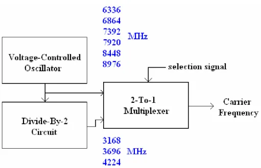
(20) Chapter 2 Wideband Voltage-Controlled Oscillator and Its Frequency Divider for MB-OFDM UWB system. In this chapter, a wide tuning range voltage-controlled oscillator (VCO) and a divider-by-2 circuit are combined together to fulfill a local oscillator for the UWB system application. Besides, a 2-to-1 multiplexer is used to select which path the output signal is from. This circuit is implemented in TSMC RF 1P6M 0.18 μm CMOS technology and fabricated in February 2006. In the following sections, three blocks of this circuit will be explained individually. In addition, both the simulation and measurement results will also be discussed.. 2.1 Circuit Design Consideration In MB-OFDM UWB system, carrier frequencies are distributed in a spectrum of 3.1~10.6 GHz and with 528 MHz apart from each other. To meet this specification a voltage-controlled oscillator is necessary to have very wide tuning range. However, it’s difficult for LC-VCO to cover such a wide range. Therefore a 6~9 GHz VCO and its frequency divider are designed to provide carrier frequencies for Band Group #1, #3 and #4 in MB-OFDM UWB system[3]. The Band Group #2 is bypassed because occupied by 802.11a and HiperLAN devices. The architecture is shown in Fig. 2-1. 8.
(21) Fig. 2-1 Architecture of VCO and its divider. 2.1.1 Multi-Band Voltage-Controlled Oscillator The model of LC-resonant oscillators is shown in Fig. 2-2. The oscillation frequency is decided by the equivalent inductance Leq and capacitance Ceq in the tank. For the purpose of frequency tuning, it is common to use varactors which can vary Ceq in LC-resonant oscillators. The tuning range has to be very wide to meet the UWB system specification. Unfortunately the noise on the control voltage translates into phase noise and wider tuning range makes this problem more serious. Moreover, the size of the varactors has to be increased and the nonlinearity of larger varactors converts more amplitude noise into phase noise. Therefore, the SCA (Switched-Capacitor-Array) is added to avoid using large varactors[6][7]. Another advantage of SCA is that MIM (metal-insulator-metal) capacitors have a higher Q-value (about 1000) than varactors do. Due to this SCA design characteristic, the noise performance is improved. Fig. 2-3 shows the schematic of this multi-band VCO.. 9.
(22) Fig. 2-2 Model of the ideal LC-resonant oscillator. Fig. 2-3 Voltage-controlled oscillator and the switched-capacitor-array This VCO adopts a complementary cross-coupled negative-gm configuration which has several benefits: (1) only one inductor is needed and large chip area is saved (2) smaller voltage drop across the MOS transistors reduces the effect of velocity saturation in the short channel regime (3) the complementary structure offers higher trans-conductance for a given current, which results in fast switching of the cross-coupled pair (4) the output swing is more symmetry to alleviate the noise up-conversion effect and then phase noise performance is improved[8]. In addition, the current source is in parallel with a capacitor which provides a path to remove the noise disturbance from the current source. For symmetry the capacitor is actually placed at both sides of the current source.. 10.
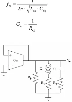
(23) The SCA (switched-capacitor-array) is formed with four pairs of binary-weighted MIM capacitors and four MOS transistors as digital-control switches. But actually the term 2C is replaced for the original term 8C because the bandwidth is already sufficient and using larger capacitors means increasing the load. The SCA provides coarse tuning while the varactors are in charge of fine tuning. In other words, the digital-control signal (B0, B1, B2, and B3) decides that which band the oscillation frequency is in and then analog-control voltage (Vctrl) controls the actual oscillation frequency. According to the rule mentioned above, the requirement for varactors is relaxed because the varactors are not responsible for the whole bandwidth. Fig. 2-4 shows the SCA modification. The MOS switches are not directly connected to the ground, and instead they are connected to both capacitors. This topology can avoid the substrate noise coupling into the tank and halve the number of the MOS switches. Therefore the on-resistance can be reduced and phase noise is improved. The inverted digital-control signals assure that both gate-source and gate-drain junctions are reverse-biased in the OFF state and vice versa[9]. As a result, the effective capacitance of SCA is: 3. C eff = ∑ Bi ⋅ i =0. Ci 2. ( 2-1 ). Fig. 2-4 (a) The conventional SCA and (B) the adopted SCA in this circuit According to Fig. 2-2, the topology of LC-resonant oscillators is positive feedback. For the sake of stable oscillation, the trans-conductance has to be large enough to restore energy dissipated in the resistance of the LC-tank. In other words, the impedance of the active network should be equal to –Reff and the unity loop gain is achieved[10]. Consequently, the 11.
(24) oscillation frequency and required trans-conductance are: ( 2-2 ). 1. fO =. 2π ⋅ Leq ⋅ C eq Gm =. 1 Reff. ( 2-3 ). Fig. 2-5 Model of the LC-resonant oscillator with parasitic resistance In regard to low power consumption, the bias current is supposed to be small and then trans-conductance shrinks. As a result, the bias current should be chosen carefully. Also the overdrive voltage of the cross-coupled transistors needs prudent consideration to accomplish a good compromise between phase noise, tuning range, and power dissipation. Considering the parasitic resistance and non-ideal passive components in Fig. 2-5, the required trans-conductance can be expressed as Gm =. Rc Rl 1 1 = + + 2 2 Reff (2π ⋅ f O ⋅ L) Rp (2π ⋅ f O ⋅ L). ( 2-4 ). with fo the oscillation frequency, Rc the capacitor series resistance, Rl the inductor series resistance, and Rp the parasitic resistance. Moreover, to ensure reliable start-up, the active network has to provide 2~3 times required trans-conductance[10]. Now the bias current can be determined:. I bias = 2 I mn = 2 ⋅. g mn ⋅ VOD 2. ( 2-5 ). where Imn, gmn and VOD are the bias current, trans-conductance, and overdrive voltage of the NMOS transistors in Fig. 2-3. Finally, the phase noise can be found in the following 12.
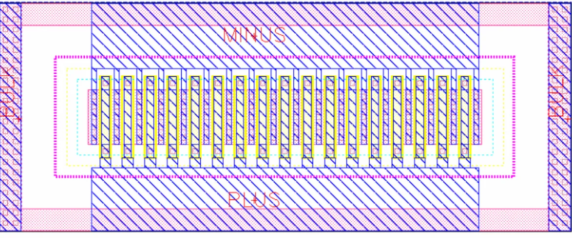
(25) expression kT ⋅ [ Rc + Rl + L{Δf } =. (2π ⋅ f O L) 2 f ] ⋅ (1 + A) ⋅ ( O ) 2 Rp Δf V A2 / 2. ( 2-6 ). where VA is the amplitude of the output swing, A is the noise contribution factor of the active network (usually equal to or larger than 1), and Δf is the offset frequency from the carrier at fo. Through Eq. ( 2-6 ), there is trade-off between power dissipation and phase noise performance. Therefore a power-frequency-normalized (PFN) figure-of-merit (FOM) is often used to compare the performance of VCOs for both power consumption and phase noise[11].. FOM = 10 ⋅ log[. kT f O 2 ⋅ ( ) ] − L{Δf } Pdis Δf. ( 2-7 ). In Eq. ( 2-7 ), Pdis is the dc power dissipation in the VCO and FOM is often expressed in dB. A greater FOM corresponds to a better oscillator. There are several new RF passive elements in TSMC RF 1P6M 0.18 μm CMOS technology. The improvement of the passive element leads to the better circuit performance. In the fully integrated VCOs, the low Q-factor LC-tank is mainly caused by the spiral inductors. Symmetric inductors have higher Q-value thanks to their geometric characteristic. The layout of the symmetric inductor in this circuit and its equivalent lumped circuit are shown in Fig. 2-6 with spacing=2 μm, width=15 μm, radius=47 μm, and 2 turns. The equivalent inductance Leq is about 0.555 nH and the parasitic resistance Rl is 1.8 Ω. In addition, the accumulation-mode MOS varactors is offered with a higher Q-value and larger capacitance variation range than diode varactor[12]. Here Fig. 2-7 shows the layout of the varactor and its equivalent lumped model. The MOS varactor has 17 branches in one group. The equivalent capacitance Ceq is about 40.8~153 fF and the parasitic resistance Rc is 6.24 Ω. After considering the SCA, VCO output stage and parasitic effect from the chip layout, the simulated VCO oscillation frequency is around 8.9 GHz. Due to the lumped models of spiral inductor and MOS varactors, the required trans-conductance and bias current can be decided 13.
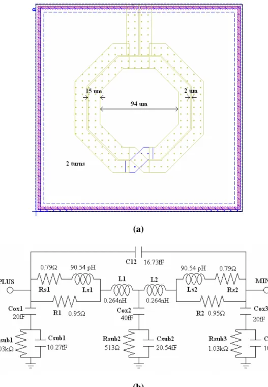
(26) by Eq. ( 2-4 )and ( 2-5 ).. Gm =. 1 (6.24 + 1.8) = = 8.16 mA / V Reff (2π ⋅ 9G ⋅ 0.555n) 2 I bias = 2 ⋅. 4.08m ⋅ 0.9 = 3.67 mA 2. Besides, it is possible that the Gm and IBIAS are a little bit insufficient owing to omitting some parasitic resistance. But it still provides a good starting point for the design.. (a). (b) Fig. 2-6 (a) Layout and (b) its lumped model of the symmetric spiral inductor 14.
(27) (a). (b) Fig. 2-7 (a) Layout and (b) its lumped model of the MOS varactor. 2.1.2 High Frequency Divider Frequency dividers operating at high frequency are one of the key blocks in the RF circuits because dividers must function properly over the required bandwidth and provide enough output swing for the next stage. Three kinds of dividers are often used: digital CMOS logic, current-mode logic (CML), and injection-locked frequency dividers (ILFD)[13]. Digital CMOS logic is seldom used since full-scale swing is needed and the operating frequency is relatively low. Compared with CML, ILFD has lower power consumption with larger area and. 15.
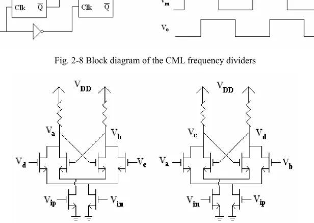
(28) narrower locking range. Due to very wide bandwidth of VCO, the CML is chosen in this work[14].. Fig. 2-8 Block diagram of the CML frequency dividers. Fig. 2-9 Schematic of the CML frequency dividers The block diagram of CML frequency dividers is shown in Fig. 2-8. The frequency of both Vm and Vo is half the frequency of Vi. Meanwhile the phase difference between Vm and Vo is just 90 degree and quadrature outputs are obtained. In other words, CML is also a kind of quadrature signal generators owing to the characteristic of the output nodes. According to Fig. 2-9, the master and slave D-FFs (D-type flip-flop) are clocked by complementary clocked signals and the differential outputs of LC-VCO in the previous section provide this kind of input signals. Consequently, the inverter in Fig. 2-8 is implemented without adding any circuit. The D-FFs implemented in CML are composed of a clocked differential sensing amplifier pair and inversely clocked latching pair. In contrast with common CML circuits, the bias current source is eliminated to increase the maximum operating frequency about 10 %[15]. 16.
(29) Only NMOS transistors are used in this circuit because the drain parasitic capacitance and power dissipation should be minimized. Due to omitting the current source, the bias point of this divider is determined by the DC level of the input signals, the size of the clock transistors and the load resistance. The trans-conductance of clock transistors has to be large and then the small input signals can drive them from the linear region to the saturation region. Therefore the sensitivity to the DC level of input signals is increased. The load resistance is another key parameter since the dominant pole is decided by the load resistance and parasitic capacitance from transistors, interconnection, and next stage. As a result, the load resistance has to be kept small to make the dominant pole high enough and it is inevitable to raise the bias current to assure the next stage of proper DC input level.. (a). (b). Fig. 2-10 Schematic of (a) the latching pair and (b) the sensing pair. 17.
(30) Fig. 2-11 Comparison of amplification in (a) the latching and (b) the sensing As shown in Fig. 2-10, the latching pair works in positive-feedback regeneration while sensing pair is in common-source configuration. latching pair :. Vo (t ) g R −1 = exp( m ⋅ t) Vo (0) RC. ( 2-8 ). sensing pair :. Vo (t ) −t )] = g m R ⋅ [1 − exp( RC Vi (t ). ( 2-9 ). According to Eq. ( 2-8 ) and ( 2-9 ), Fig. 2-11 is plotted under the same condition. The latching pair boosts the output exponentially while the sensing pair is an approximately linear amplifier. When the trans-conductance of latching pair is large, the latching is fast but changing state is difficult. Additionally, the clock is fed by sinusoidal signal rather than square wave. The grey area is wider between latching and sensing. In consequence the size of the sensing pair transistors has to be a bit greater than the size of the latching pair ones.. 18.
(31) 2.1.3 2-to-1 Multiplexer. Fig. 2-12 Schematic of the 2-to-1 multiplexer In the beginning of this chapter, it is mentioned that a multi-band VCO provides carrier frequencies in Band Group #3 and #4 while a frequency divider is in charge of frequencies in Band Group #1 for the MB-OFDM UWB system. As a result, there is a 2-to1 multiplexer to decide that the output is generated from VCO or the divider. Fig. 2-12 shows the schematic of the multiplexer. Again the current source is removed to relax the voltage headroom problem[16]. When Vsel is high, MS2 is off and the output is only from the VCO. On the contrary, when Vsel is low, MS1 is off and the output is only from the divider. Because the output signals are spread in a very wide range of spectrum, the gain must be insensitive to the operating frequency. The load inductors and capacitors should be designed as large as possible to alleviate the impedance variation with the frequency. Therefore the bias-tee is chosen as the load impedance. The inductor and capacitor in the bias-tee can be treated as infinitely large at the multi-GHz frequency. For this reason, the load impedance is approximately only RL (50 ohm). The pure-resistive impedance fulfills a gain without dependency of the operating frequency. In MB-OFDM UWB system, the channel switching time is about only 9.5 nsec. As a result, the multiplexer must change the output signals in a time less than the required period. Because MS1 and MS2 work as complementary switches, the length of these two transistors is 19.
(32) kept the minimum value and the width is supposed to be a reasonable value to compromise between parasitic capacitance and trans-conductance.. 2.2 Chip Layout and Simulation Results A signal generator for UWB system is designed and optimized through Eldo RF simulator. The whole chip is 0.83×1.12 mm2 and fabricated in TSMC RF 1P6M 0.18 μm CMOS technology. Fig. 2-13 is the layout of this circuit. In order to extract the parasitic effect from the interconnection, Calibre xRC is adopted for the post-simulation. However it is insufficient to consider parasitic capacitance and resistance only. Parasitic inductance accompanies the interconnections in the circuits operating at multi-GHz band. Consequently, Sonnet software is also used to convert critical parts of the layout into s-parameter files and the interconnections are treated as transmission lines. Several parts of the whole chip are processed by Sonnet software and Fig. 2-14 shows one example. Besides, the layout should be kept symmetry to equalize the amplitude of the differential outputs. The power dissipation of each block is listed in Table 2-1. As shown in Fig. 2-15, the tuning range is 5.97~9.22 GHz (about 42.8% of the center frequency) for the total 10 curves. A particular digital-control signal obtains its corresponding curve. Overlapping between curves is necessary to cover the entire band. In the lower bands, the slopes of these tuning curves and the distances between curves are smaller. The following equation can prove this. f1 =. 1 LC. Δf = f1 − f 2 = =. f2 =. 1. L(C + ΔC ) 1 1 [1 − ]≅ LC (1 + ΔC / C ). 1 LC. [1 − (1 −. ΔC LC 2C 1. ⋅. 20. ΔC )] 2C. (Assumes ΔC<<C). ( 2-10 ).
(33) Due to larger capacitance in the lower bands, Δf becomes smaller. In other words, the oscillation frequencies in the lower band don’t vary as much as those in the higher bands.. Fig. 2-13 Layout of the whole chip. (a). 21.
(34) (b) Fig. 2-14 (a) Imported layout and (b) extracted S-parameter in Sonnet software Table 2-1 Power dissipation of each blocks in this circuit Power. Current. VCO. 7.09 mW. 3.94 mA. divider. 9.43 mW. 5.24 mA. multiplexer. 21.39 mW. 11.88 mA. total. 37.91 mW. 21.06 mA. Fig. 2-15 Tuning range curves of VCO with different banks 22.
(35) When the control voltage is 1.05 V with digital input (0,0,0,0), the oscillation frequency is 8.976 GHz. The output swing is 0.95 VPP (3.53 dBm) and the phase noise is -111 dBc/Hz at 1 MHz offset. Through the frequency divider, another signal at 4.488 GHz is also generated. These results are shown in Fig. 2-16 and Fig. 2-17.. Fig. 2-16 Output waveform of VCO and frequency divider. Fig. 2-17 Phase noise with oscillation frequency at 8.976 GHz 23.
(36) When the control voltage is 0.98 V with digital input (0,0,0,1), the oscillation frequency is 8.448 GHz. The output swing is 0.86 VPP (2.67 dBm) and the phase noise is -111 dBc/Hz at 1 MHz offset. Through the frequency divider, another signal at 4.224 GHz is also generated. These results are shown in Fig. 2-18 and Fig. 2-19.. Fig. 2-18 Output waveform of VCO and frequency divider. Fig. 2-19 Phase noise with oscillation frequency at 8.448 GHz 24.
(37) When the control voltage is 0.77 V with digital input (0,0,1,0), the oscillation frequency is 7.92 GHz. The output swing is 0.82 VPP (2.26 dBm) and the phase noise is -112 dBc/Hz at 1 MHz offset. Through the frequency divider, another signal at 3.96 GHz is also generated. These results are shown in Fig. 2-20 and Fig. 2-21.. Fig. 2-20 Output waveform of VCO and frequency divider. Fig. 2-21 Phase noise with oscillation frequency at 7.92 GHz 25.
(38) When the control voltage is 1.47 V with digital input (1,0,0,0), the oscillation frequency is 7.392 GHz. The output swing is 0.8 VPP (2.04 dBm) and the phase noise is -113 dBc/Hz at 1 MHz offset. Through the frequency divider, another signal at 3.696 GHz is also generated. These results are shown in Fig. 2-22 and Fig. 2-23.. Fig. 2-22 Output waveform of VCO and frequency divider. Fig. 2-23 Phase noise with oscillation frequency at 7.392 GHz 26.
(39) When the control voltage is 0.5 V with digital input (1,0,0,1), the oscillation frequency is 6.864 GHz. The output swing is 0.7 VPP (0.88 dBm) and the phase noise is -114 dBc/Hz at 1 MHz offset. Through the frequency divider, another signal at 3.432 GHz is also generated. These results are shown in Fig. 2-24 and Fig. 2-25.. Fig. 2-24 Output waveform of VCO and frequency divider. Fig. 2-25 Phase noise with oscillation frequency at 6.864 GHz 27.
(40) When the control voltage is 1.27 V with digital input (1,1,1,0), the oscillation frequency is 6.336 GHz. The output swing is 0.64 VPP (0.1 dBm) and the phase noise is -113 dBc/Hz at 1 MHz offset. Through the frequency divider, another signal at 3.168 GHz is also generated. These results are shown in Fig. 2-26 and Fig. 2-27. Finally, the output power and the phase noise are listed for all carrier frequencies in Table 2-2.. Fig. 2-26 Output waveform of VCO and frequency divider. Fig. 2-27 Phase noise with oscillation frequency at 6.336 GHz 28.
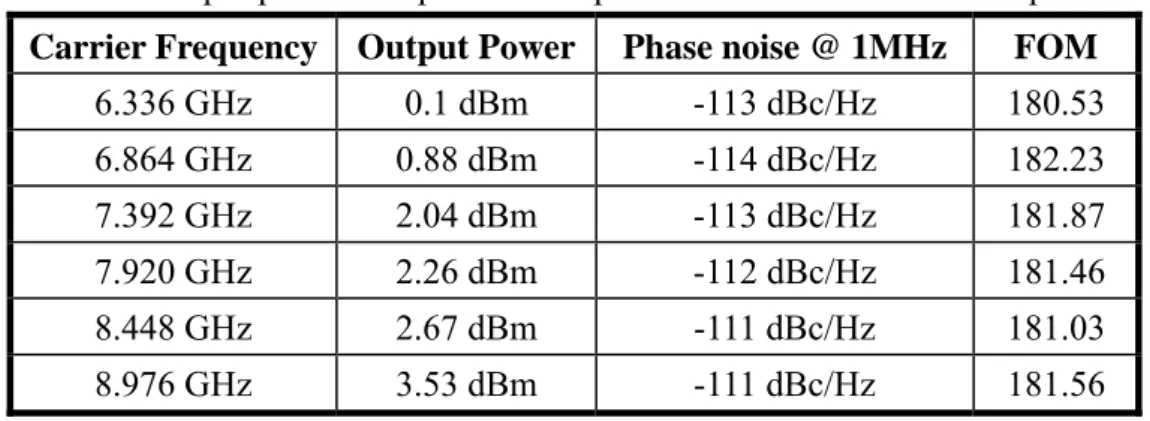
(41) Table 2-2 Output power and phase noise performance of the carrier frequencies Carrier Frequency. Output Power. Phase noise @ 1MHz. FOM. 6.336 GHz. 0.1 dBm. -113 dBc/Hz. 180.53. 6.864 GHz. 0.88 dBm. -114 dBc/Hz. 182.23. 7.392 GHz. 2.04 dBm. -113 dBc/Hz. 181.87. 7.920 GHz. 2.26 dBm. -112 dBc/Hz. 181.46. 8.448 GHz. 2.67 dBm. -111 dBc/Hz. 181.03. 8.976 GHz. 3.53 dBm. -111 dBc/Hz. 181.56. Because the 2-to-1 multiplexer is in charge of the output signals from VCO or the frequency divider, its bandwidth and switching time are important parameters. A very large bandwidth (10M~10GHz) is achieved in Fig. 2-28. According to Fig. 2-29, the switching period is 0.8 nsec when the multiplexer changes the output from VCO to the divider. Furthermore, the band switching in the VCO also needs to be short enough. In Fig. 2-30, the band switching is completed in about 0.65 nsec. In consequence, both of the periods are much shorter than the required time (9.5 nsec).. Fig. 2-28 Gain of the multiplexer vs. the input frequency. 29.
(42) Fig. 2-29 Output waveform switching from VCO to the divider. Fig. 2-30 Output waveform switching from bank (1,1,1,1) to bank (0,0,0,0) The simulation also considers PVT (process-voltage-temperature) corner variations. The tuning range curves are simulated under different conditions. The results are shown in Fig. 2-31~Fig. 2-36 and summarized in Table 2-3. The curves are almost invariant regardless of any corner variation.. 30.
(43) Fig. 2-31 Tuning range curves at FF corner. Fig. 2-32 Tuning range curves at SS corner. 31.
(44) Fig. 2-33 Tuning range curves at VDD=1.62 V. Fig. 2-34 Tuning range curves at VDD=1.98 V. 32.
(45) Fig. 2-35 Tuning range curves at T=-10°C. Fig. 2-36 Tuning range curves at T=60°C. 33.
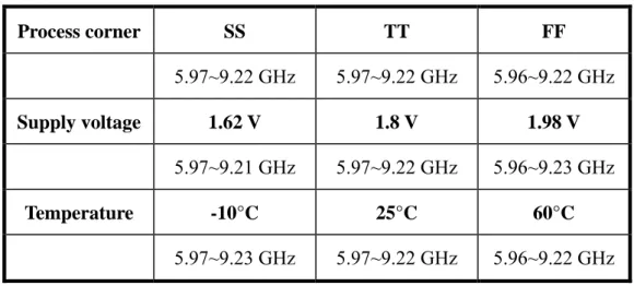
(46) Table 2-3 VCO tuning range under different conditions Process corner. Supply voltage. Temperature. SS. TT. FF. 5.97~9.22 GHz. 5.97~9.22 GHz. 5.96~9.22 GHz. 1.62 V. 1.8 V. 1.98 V. 5.97~9.21 GHz. 5.97~9.22 GHz. 5.96~9.23 GHz. -10°C. 25°C. 60°C. 5.97~9.23 GHz. 5.97~9.22 GHz. 5.96~9.22 GHz. 2.3 Measurement Results The results are obtained from on wafer circuit measurement in National Chip Implementation Center (CIC). The instruments contain Agilent E5052A signal source analyzer, E4407B spectrum analyzer, and E3615A DC power supply in Fig. 2-37. Also the whole chip photograph is shown in Fig. 2-38.. (a). 34.
(47) (b). (c). (d) Fig. 2-37 Measurement instruments (a) Agilent E5052A signal source analyzer (b) E4407B spectrum analyzer (c)E3615A DC power supply and (d) whole test set 35.
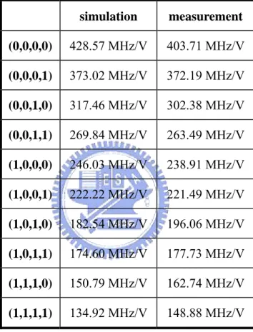
(48) Fig. 2-38 Chip photograph. Fig. 2-39 Measured tuning range curves with different banks. 36.
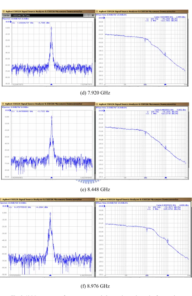
(49) According to Fig. 2-39, the 10 tuning range curves cover each other and signal at 6.12~9.15 GHz can all be generated. This range includes the whole required bandwidth. Comparing with 5.97~9.22 GHz bandwidth in the simulation results, the total tuning range is a little shrunk. Because the gain of the VCO is little changed in Table 2-4, the compressed tuning range is mainly from the overestimated capacitors in SCA. Table 2-4 KVCO Comparison between the simulation and the measurement result simulation. measurement. (0,0,0,0). 428.57 MHz/V. 403.71 MHz/V. (0,0,0,1). 373.02 MHz/V. 372.19 MHz/V. (0,0,1,0). 317.46 MHz/V. 302.38 MHz/V. (0,0,1,1). 269.84 MHz/V. 263.49 MHz/V. (1,0,0,0). 246.03 MHz/V. 238.91 MHz/V. (1,0,0,1). 222.22 MHz/V. 221.49 MHz/V. (1,0,1,0). 182.54 MHz/V. 196.06 MHz/V. (1,0,1,1). 174.60 MHz/V. 177.73 MHz/V. (1,1,1,0). 150.79 MHz/V. 162.74 MHz/V. (1,1,1,1). 134.92 MHz/V. 148.88 MHz/V. Following the tuning range, the output power and phase noise performance is measured in Fig. 2-40 and Table 2-5. The measured value of the phase noise is approximately equal to the simulated one while the output power is about 5 dB smaller than the simulation result. This is probably caused by the loss of the coaxial line. Especially two series coaxial lines are connected for the longer distance between the chip and the instruments. According to data in CIC, the loss is compensated and actual output power is obtained. Therefore, the signal attenuation can be considerable. 37.
(50) (a) 6.336 GHz. (b) 6.864 GHz. (c) 7.392 GHz. 38.
(51) (d) 7.920 GHz. (e) 8.448 GHz. (f) 8.976 GHz Fig. 2-40 Measurement of output power and phase noise at six carrier frequencies. 39.
(52) Table 2-5 Measurement of output power and phase noise performance at six frequencies Carrier Frequency. Output Power. Phase noise @ 1MHz. FOM. 6.336 GHz. -5.85 dBm. -114.96 dBc/Hz. 182.49. 6.864 GHz. -1.08 dBm. -115.08 dBc/Hz. 183.31. 7.392 GHz. -1.33 dBm. -111.80 dBc/Hz. 180.67. 7.920 GHz. -0.99 dBm. -112.35 dBc/Hz. 181.81. 8.448 GHz. -1.17 dBm. -113.07 dBc/Hz. 183.10. 8.976 GHz. -1.54 dBm. -105.47 dBc/Hz. 176.03. Besides the VCO, the performance of the divider-by-2 circuit is measured in Fig. 2-41. The multiplexer suppresses the VCO signal about 20 dB when the frequency divider is selected. But at 4.224 GHz the divider doesn’t work properly in Fig. 2-42. The reason is likely that the parasitic effect at the output nodes of the divider is not completely extracted and the behavior can’t be accurately predicted in the post-simulation. As a result, the control voltage of VCO is tuned and the locking range of the frequency divider is up to 7.84 GHz. The measurement is shown in Fig. 2-43. Finally, the power dissipation in the measurement is very close to the result in the simulation.. (a). (b). Fig. 2-41 Output power of the carrier frequency at (a) 3.168 and (b) 3.696 GHz. 40.
(53) (a). (b). Fig. 2-42 MUX output at 4.224 GHz when (a) the divider or (b) VCO is selected. Fig. 2-43 Maximal frequency in the locking range of the divider. 2.4 Summary and Comparison The performance in the measurement is close to the results in the simulation except that 4.224 GHz signal is not generated successfully. To improve this, the layout parasitic extraction by EM software has to be more detailed although this will take a far longer time. The summary of this work is listed in Table 2-6. In addition, the comparison with other wideband VCOs is made in Table 2-7. Through the figure-of-merit (FOM), this work really achieves better performance. 41.
(54) Table 2-6 Summary of the performance in the simulation and measurement Performance. Post-Simulation. Measurement 1.8V. Supply Voltage Power Consumption. 37.91 mW. 36.63 mW. Tuning Range. 5.97~9.22 GHz. 6.12~9.15 GHz. Phase Noise @ 1MHz. -111~-114 dBc/Hz. -105.5~-115 dBc/Hz. Output Power. 0.1~3.53 dBm. -5.85~-0.99 dBm. Table 2-7 Comparison with the recent published papers about wideband VCOs MAPE 2005. MWCL 2005. ISCAS 2005. This Work. [17]. [18]. [19]. Technology. 0.35 μm SiGe. 0.18 μm CMOS. 0.18 μm CMOS. 0.18 μm CMOS. Supply. 3V. 1.8 V. 1.5 V. 1.8 V. Tuning. 2.08~2.51 GHz. 5.5~6.7 GHz. 3.5~5.3 GHz. 6.12~9.15 GHz. Range. 430 MHz, 17.6%. 1.2 GHz, 20%. 1.8 GHz, 40.9%. 3 GHz, 39.7%. Phase. -110 dBc/Hz. -115 dBc/Hz. -115 dBc/Hz. -115 dBc/Hz. Noise. @ 1 MHz. @ 1MHz. @ 1 MHz. @ 1 MHz. Power. 12.06 mW. 5.8 mW. 6 mW. 36.63 mW. Voltage. (7.09 mW in. Dissipation. VCO core) FOM. 166.97. 182.17. 42. 180.09. 183.31.
(55) Chapter 3 Low Power and Fast-Locking Integer-N Frequency Synthesizer for MB-OFDM UWB System. In this chapter, a low power and fast-locking integer-N frequency synthesizer is presented for the MB-OFDM UWB application. Because of the frequency divider in this proposed synthesizer, a remarkable reduction in the power dissipation is achieved. Additionally, the choice of the reference clock leads immunity against the spurious tone. This circuit is designed by using TSMC RF 1P6M 0.18 μm CMOS technology and applied to be fabricated in June 2006. In the following sections, the architecture and circuit design consideration is demonstrated first. Then each block in this frequency synthesizer will be explained individually. Finally, the simulation results and comparison will also be discussed.. 3.1 Architecture There are three ways to perform frequency generation for MB-OFDM UWB system. One approach is to have multiple PLLs in parallel which are responsible for different frequencies. In [20], three fixed-modulus PLLs are used for the frequencies in Band Group #1. This method is most direct and easy to meet the specifications. However, it will need too many PLLs while all 14 carrier frequencies are used. It will demand too much power dissipation and large chip area to be practical. The second method is to integrate PLLs with external multiplexers and single side-band (SSB) mixers[21]-[23]. Two specified frequencies are 43.
(56) generated by PLLs and SSB mixers can up/down-convert these two signals into the desired carrier frequency. But the SSB mixers need accurate quadrature inputs and should be highly linear for low spurious tones. These requirements add more complexity and difficulty to the circuits. The third method is using two fast-settling frequency synthesizers to generate the desired signal by turns[24]. As proposed in [3], the symbol interval is 312.5 nsec and the guard time is 9.47 nsec. Therefore a single PLL has to be locked with about 322 nsec. It becomes more practical for a conventional frequency synthesizer which is easy to be implemented. Here the third method is adopted in this thesis.. Fig. 3-1 Block diagram of the synthesizer in [24]. Fig. 3-2 Block diagram of the proposed synthesizer As shown in Fig. 3-2, QVCO in the proposed synthesizer does not have to generate all signals for whole 3.1~10.6 GHz band. In fact, QVCO is merely responsible for Band Group #3 and #4 while Band Group #1 is left for the divider-by-2 circuit. Band Group #2 is ignored 44.
(57) for the better coexistence with other wireless standards and Band Group #5 is reserved for the future research. Comparing with [24], there are several modifications in this proposed synthesizer. First, the divider-by-2 circuit is included in the loop. In [24], the dual-modulus /4/5 divider contains six CML DFFs which are power-hungry when operating at high frequencies from QVCO. Therefore it is replaced by a divider-by-2 circuit which consumes less than half original power (including the external divider-by-2) and the load of the oscillator becomes smaller because only two DFFs are needed. Second, two dual-modulus /2/3 dividers are substituted for the /4/5 divider. This reduces the power in the multi-modulus divider again. Section 3.2.2 will give explanation for why the power reduction is made. Third, the frequency of the reference clock is halved. Although this causes the settling time longer, the specification is still met. Moreover the reference frequency is half of the channel bandwidth and then the spur effect on the channel is eliminated. It is resulted from that spurs occur at the center of two neighboring channels and do not pollute the channel anymore (shown in Fig. 3-3). The requirement of the spurious tones is greatly relaxed.. Fig. 3-3 Comparison of spur at different frequencies. 3.2 Circuit Design Consideration According to Fig. 3-2, the proposed frequency synthesizer is based on an integer-N type. 45.
(58) phase-locked loop. In contrast with fractional-N type, integer-N type has a fixed division number in every reference clock and then spurious tone is lowered. In addition, it is a simpler structure and dissipates less power. Due to the relatively large frequency resolution (528 MHz) and sufficient locking time, integer-N type is more suitable in this design. This frequency synthesizer is composed of a quadrature voltage-controlled oscillator (QVCO), a multi-modulus frequency divider, a fast phase-frequency detector, a charge pump with variable current, and an on-chip third-order passive loop filter. There are seven digital input signals: four are to select the tuning range curves of the QVCO and the remainders are to control the division ratio in the multi-modulus divider. As mentioned in the preceding section, the frequency synthesizer has to settle with 322 nsec over PVT (process-voltage-temperature) corner variations. Therefore the settling time is designed to be approximately 200 nsec. The essential open-loop bandwidth to achieve a settling time of 200 nsec can be roughly calculated by the following equation BW =. f step 1 ⋅ ln( ) Tlock ζ e ( PM ) f error. ( 3-1 ). where Tlock is the locking time, ζe(PM) is the effective damping coefficient as a function of the loop phase margin PM, fstep is the magnitude of the frequency jump, and ferror is the allowable frequency error after locking[25]. This equation is derived from continuous-time approximation. As far as the fastest locking time is concerned, the phase margin should be set to 50°, and ζe(50°) will be about 5[26]. In the case of 528 MHz frequency jump and 1 KHz frequency error tolerance, BW is about 13.2 MHz from Eq. ( 3-1 ). In a PLL design, the reference frequency has to be greater than 10 times of the loop bandwidth in order to guarantee the loop stability[27]. In other words, the assumption of the 264 MHz reference frequency above is quite acceptable. Although the frequency of a conventional crystal oscillator is merely up to tens MHz, a simple PLL can be employed for the synthesis of the reference clock for the consideration of SOC. A narrow band PLL is preferred because phase. 46.
(59) noise at an offset above a few hundred kHz has to as low as possible. In the principle of designing PLLs, wider loop bandwidth leads to more suppression of the in-band VCO phase noise. As a result, noise from other blocks, such as reference, charge pump, and loop filter becomes more important within the loop bandwidth. By the UWB system proposal, the noise requirement is defined as the overall integrated rms phase noise from 0 Hz to infinity and the obtained value should be lower than 3.5°. This integrated phase noise can be calculated by this formula: rms noise =. 180. π. ⋅ 10 0.05 k BW ⋅ (1 + 10 0.1 p ) + 2 ⋅ 10 0.1 p. ( 3-2). where k is the in-band phase noise density (dBc/Hz) and p is the peaking of k[24]. In order to achieve the integrated phase noise below 3.5°, k should be less than -95.5 dBc/Hz while p is assumed to be 0. Spurious tones from the ripple on the QVCO control voltage do not get much attenuation by the loop filter because of the wide bandwidth. To reduce these spurious tones can be accomplished by matching the current sources in the charge pump. At the output nodes of QVCO, the relative magnitude of the primary sidebands is given by: spur =. Aripple ⋅ K V 2 ⋅ 2π ⋅ f REF. ( 3-3 ). where Aripple is the peak amplitude of the first harmonic of the ripple, KV is the gain of the QVCO, and fREF is the reference frequency[29]. For smaller spurious tones, Aripple and KV should be minimized. Current matching in the charge pump is a method to lower Aripple. KV should be as small as possible while the tuning range still meets the specification. In this circuit, KV is large and up to 500 MHz/V because a 6~9 GHz band needs to be covered. Under the condition of the maximal KV and the given 264 MHz reference frequency, the peak fundamental ripple amplitude must be less 10.6 mV to guarantee than sidebands are 50 dB below the carrier. The output frequency is determined by the multi-modulus frequency divider. The 47.
(60) division factor is controllable even number from 24 to 34. The frequency synthesizer can provide six carrier frequencies which are spread from 6.336 to 8.976 GHz in steps of 528 MHz.. 3.2.1 Quadrature Voltage-Controlled Oscillator There are several ways to obtain quadrature signals: divider-by-2 circuit, RC poly-phase filters, and two interleaved voltage-controlled oscillators. The divider-by-2 circuit needs an oscillator operating at 2 times higher than the desired frequency and a high-speed frequency divider. Both circuits dissipate a lot of power in spite of a smaller chip size. RC poly-phase filters attenuate the signal and increase the effective capacitance of the tank. Also a lot of chip area is needed for a good matching of the filters. For the low power consumption and quadrature phase accuracy, two interleaved voltage-controlled oscillators are adopted in this circuit[28]. According to the Barkhausen criterion, oscillation occurs only when the loop gain [A(jω)]4 is unity in Fig. 3-4. Therefore A(jω) has amplitude of one with a 90 degree phase shift and quadrature signals are obtained at the four outputs of these two VCOs.. Fig. 3-4 Two interleaved VCO configuration As shown in Fig. 3-5(a), the VCO is in a complementary cross-coupled negative-gm configuration. The advantages of this configuration are mentioned in Chapter 2. However, there is a difference from the VCO in Chapter 2. The tail current source is removed to. 48.
(61) maximize the output swing. Two benefits are also achieved thanks to the removal of the current source. First the current source is the main contributor to the phase noise[30]. Second, when all transistors in the VCO core are put in GHz-switching bias condition, flicker noise will apparently be reduced by about 10 dB[31]. The dimension of four cross-coupling PMOS transistors is an important parameter. If cross-coupling is made weak, two-tones oscillation exists probably; if it is made strong, DC power is wasted and more capacitance is added into the LC-tank. By means of transient simulations, the optimal width of the cross-coupling transistors should be set to one-third of the width of the core transistors while the length of all transistors is chosen as the minimal length (0.18 μm in this circuit)[32].. (a). (b). Fig. 3-5 (a) Quadrature voltage-controlled oscillator and (b) switch-capacitor array For a wide tuning range of 6~9 GHz, the SCA (switched-capacitor-array) is used as well as in Chapter 2. SCA is composed of four pairs of binary-weighted MIM capacitors and eight NMOS transistors as digital-control switches. The SCA decides the tuning range curve and then the varactors are for actual frequency. Therefore no bulky varactors are required because the whole bandwidth is not covered only by the varacters. Fig. 3-5 shows the SCA configuration. The NMOS switches are connected to ground directly rather than connected 49.
(62) with bottoms of two MIM capacitors. Despite of several advantages remarked in Chapter 2, NMOS switches connected with the MIM capacitors leads to a more complicated layout and serious parasitic effect. The passive components in LC tank are symmetric spiral inductors and accumulation-mode varactors again. They improve the phase noise performance due to their higher Q-value and the reason is mentioned in Chapter 2. The layout of the symmetric inductor in this circuit and its equivalent lumped circuit are shown in Fig. 3-6 with spacing=2 μm, width=15 μm, and radius=87 μm. The equivalent inductance Leq is about 0.43 nH and the parasitic resistance Rl is 1.49 Ω. Fig. 3-7 shows the layout of the varactor and its equivalent lumped model. The MOS varactor has 14 branches and two groups. The equivalent capacitance Ceq is about 140.29~339.33 fF and the parasitic resistance Rc is 2.53 Ω. After considering the SCA, VCO output stage and parasitic effect from the chip layout, the simulated VCO oscillation frequency is around 8.9 GHz under the condition of Vctrl=0.9 V and bank(0000). The simulated KV is distributed from 240~500 MHz/V.. (a). (b). Fig. 3-6 (a) Layout and (b) its lumped model of the symmetric spiral inductor. 50.
(63) (a). (b). Fig. 3-7 (a) Layout and (b) its lumped model of the MOS varactor. 3.2.2 Multi-Modulus Divider. Fig. 3-8 Programmable frequency Divider Block Diagram As shown in Fig. 3-8, a programmable frequency divider is implemented by cascaded a divider-by-2 circuit and three dual-modulus asynchronous frequency dividers. This design assures only the first divider works at the highest frequency and no pulse swallow counter or phase select state machine is needed. Moreover, the modulus-control signals of the last stage are produced first and given to the followed stage. Thus the delay in the critical path (the feedback of the first divider) is minimized[33]. In order to integrate the divider-by-2 into the loop, the division ratios are all even. In other words, a step increment is 2. The output frequency can be expressed by the following equation[34]. f out =. 1 f in 2 ⋅ (3 ⋅ 2 + C1 ⋅ 2 2 + C 2 ⋅ 2 + C 3) 2. ( 3-4 ). The required division numbers are distributed over 24~34 while 36 and 38 are reserved for future integration with Band Group #5.. 51.
(64) For the wideband locking-range and high reference frequency consideration, current-mode logic (CML) is adopted in the whole programmable frequency divider. The principle of divider-by-2 circuit is already described in Chapter 2. The dual-modulus /2/3 divider and its timing diagram are shown in Fig. 3-9. Every DFF is made up of master-slave latches. When MC bit is low, the output of the first DFF is always high and has no effect on the second DFF. It behaves as a divider-by-2 circuit. By contrast, when MC bit is high, the Vm can be low and delay the negative half-cycle for one input clock. Therefore the division ratio is turned into 3. The NAND logic gates in Fig. 3-9 can be combined with the DFF as shown in Fig. 3-10[14]. The advantages of this structure over the conventional dual-modulus divider are its simpler and more symmetric layout, improved speed, fully differential schematic, and no extra current for the logic gates[35]. The dual-modulus /3/4 divider functions in a similar way. In Fig. 3-11, a DFF is inserted at the output to lengthen one more reference cycle. As a result, a variable division ratio of 3 or 4 is achieved. The complete multi-modulus frequency divider is shown in Fig. 3-12. Several feedback AND gates are inserted into the feedback path of the individual divider.. Fig. 3-9 Schematic of the /2/3 divider. 52.
(65) Fig. 3-10 Circuit implementation of the NAND/flip-flop combination. Fig. 3-11 Schematic of the /3/4 divider. Fig. 3-12 Schematic of the programmable frequency divider From the schematic, the first DFF in a dual-modulus divider is only loaded with one flip-flop while the second is with more than two including the next stage. Consequently, the 53.
(66) second DFF dissipates approximately twice power as much as the first one. Additionally the consumed power in a divider is also about 50% of the one in the previous divider because the maximum operating frequency halves. According to this power scaling rule, less power of the divider in this work than [24] can be explained. Both /4/5 and /3/4 frequency dividers are required and one divider-by-2 circuit is also essential for Band Group #1 carriers in [24]. It is assumed that the weight is one for a DFF loaded with a flip-flop in the first stage. If the load doubles or the maximum operating frequency halves, the weight will alter proportionally. According to Table 3-1, power dissipation is theoretically only 45.6% of the power in [24]. The DC power reduction is accomplished indeed. Table 3-1 Theoretical comparison of power dissipation in dividers 1st stage [24]. 2nd stage. 1+2+2 (/4/5) 1+2+2 (/3/4). 3rd stage. 4th stage. total. N/A. N/A. 6+5/2=8.5. 1 (/2) This. 1 (/2). 1+2 (/2/3). 1+2 (/2/3). 1+2+2 (/3/4) 1+3/2+3/4+5/8=3.875. work. 3.2.3 Fast Phase-Frequency Detector The phase-frequency detector (PFD) compares two inputs from the reference clock and the output at the last stage of the frequency divider. The result decides that the control voltage of VCO is increasing or decreasing and then the output frequency is approaching to the desired value. A conventional tri-state PFD is widely used for the simplicity and wide comparable range of almost ±2π radians. Moreover it can detect both phase and frequency. The schematic of tri-state PFD is shown in Fig. 3-13. If REF arrives earlier, UP is triggered to high level and then reset to low level until DIV arrives; contrarily if DIV arrives earlier, DN is triggered to high level and reset to low level until REF arrives. Therefore greater phase error. 54.
(67) causes longer duration which UP or DN is at high level. The characteristic curve is plotted in Fig. 3-13. Although the comparable range is supposed to be ±2π the comparison produces wrong signals when the phase error is near ±2π practically. This non-ideal phenomenon is from the delay buffer in the reset path of the PFD which is to avoid a dead zone problem. The actually valid phase comparison range shrinks to ±|2π-Δ|. Δ can be found out by Δ = 2π ⋅ t delay ⋅ f REF. ( 3-5 ). tdelay is the delay time in the rest path and fREF is the reference frequency[36]. In a conventional design, the reference frequency is only a few MHz and Δ is small to ignore. Now the reference clock is 264 MHz and Δ becomes considerable. Therefore the control signal will not monotonically approach to lock-in range and the settling slows. While Δ is even larger than π, the possibility of incorrect comparisons is over 50% and the locking behavior may not be guaranteed anymore. In this case tdelay is about 312 psec and Δ is 0.16π. This value can increase the setting time to some extent.. Fig. 3-13 Schematic and characteristic of a conventional PFD. Fig. 3-14 Topology of TSPC-based DFF 55.
數據
+7
相關文件
Department of Physics and Institute of nanoscience, NCHU, Taiwan School of Physics and Engineering, Zhengzhou University, Henan.. International Laboratory for Quantum
Abstract - A 0.18 μm CMOS low noise amplifier using RC- feedback topology is proposed with optimized matching, gain, noise, linearity and area for UWB applications.. Good
Finally, making the equivalent circuits and filter prototypes matched, six step impedance filters could be designed, and simulated each filter with Series IV and Sonnet program
首先考慮針對 14m 長之單樁的檢測反應。如圖 3.14 所示為其速 度反應歷時曲線。將其訊號以快速傅立葉轉換送至頻率域再將如圖
我們分別以兩種不同作法來進行模擬,再將模擬結果分別以圖 3.11 與圖 3.12 來 表示,其中,圖 3.11 之模擬結果是按照 IEEE 802.11a 中正交分頻多工符碼(OFDM symbol)的安排,以
Jones, "Rapid Object Detection Using a Boosted Cascade of Simple Features," IEEE Computer Society Conference on Computer Vision and Pattern Recognition,
近年來,隨著無線射頻辨識技術(Radio Frequency Identification, RFID)的純熟及成 本逐漸的降低,使得全球的市場紛紛鎖定使用 RFID
指令脈波分倍頻 分倍頻 A/B 1/1,000 < A/B < 1,000 設定範圍 A :1~65,535 B :1~65,535. 内部位置指令
