國 立 交 通 大 學
電信工程學系碩士班
碩 士 論 文
全積體化低電壓低功率之 CMOS
電壓控制振盪器設計
A Fully Integrated CMOS LC-VCO with
Low Voltage and Low Power
研 究 生:黃俊諺
指導教授:唐震寰 博士
中 華 民 國 九 十 七 年 七 月
全積體化、低電壓、低功率之 CMOS 電壓控制振盪器設計
A Fully Integrated CMOS LC-VCO with Low Voltage Low Power
研 究 生:黃俊諺 Student:Jun-Yen Huang
指導教授:唐震寰 教授 Advisor:Jenn-Hwan Tarng
國 立 交 通 大 學
電 信 工 程 學 系 碩 士 班
碩 士 論 文
A ThesisSubmitted to Department of Communication Engineering College of Electrical Engineering and Computer Science
National Chiao Tung University in Partial Fulfillment of the Requirements
for the Degree of Master
in
Communication Engineering
July 2008
Hsinchu, Taiwan, Republic of China
全積體化低功率低電壓之 CMOS
電壓控制振盪器設計
研究生:黃俊諺 指導教授:唐震寰
國立交通大學
電信工程學系 碩士班
摘要
在目前無線通訊技術系統快速發展之下,研發低成本、高效能、低功耗之無 線射頻積體電路日益迫切。過去,因其在高頻的高效能之原因,射頻前端電路多 採用矽鍺(Silicon Germanium;SiGe)BiCMOS為主流製程,然而隨著標準CMOS 製程技術日趨成熟,目前採用此製程之比重已逐年提高,預計在2009年時,將約 有40%的射頻收發機電路改採CMOS製程技術。由於CMOS製程早已導入基頻晶 片多年,若是射頻電路也採用相同製程,將有助於晶片之整合,在成本降低、整 合度提高之驅動下,將掀起無線通訊市場之另一波成長;另外,在手持行動裝置 中,因射頻前端電路為最耗電之其中一部分,使得電源供應無法長效使用,尤其 在輕薄短小之目標下,功耗問題往往限制了其應用發展,因此,研發更具成本效 益的電路同時達到低功耗的目的,將是迫於解決的問題。本篇論文的研究焦點著 重於降低電壓控制振盪器其供應電壓及功率消耗之設計,同時在低功耗程度維持 一定的相位雜訊水準。利用傳統交叉對耦式的架構,以最少疊接級數中增加一對NMOS平行於電感電容共振腔,其提供的寄生電容Cgs、Cgd與交叉對耦電晶體產 生額外負電導,此負電導與等效電容可有效降低相位雜訊,另外,我們在此NMOS 之基體端加上偏壓,此一步驟將與可變電容器產生共軛壓差,進而降低共模雜 訊,同時,因此NMOS以閘極端連接共振腔,故不增加額外壓降及直流功耗,使 在最少疊接級數中能將電壓完全供應給後級的交叉對耦電晶體,達到低電壓、低 功耗目的。由量測結果(TSMC 0.18-μm 1P6M CMOS 製程),在距離中心頻率 1-MHz相位雜訊為-112.24dBc/Hz。此設計的供應電壓為0.51V,消耗功率為1 mW,其工作頻率為3.3GHz,晶片面積為0.61(μm)×0.76(μm)。
Fully Integrated CMOS LC-VCO with
Low Voltage Low Power
Student:Jun-Yen Huang Advisor:Dr. Jenn-Hwan Tarng
Department of Communication Engineering
National Chiao Tung University
Abstract
As the advancement of wireless communication system growing rapidly. Development of radio frequency (RF) integrated circuits in low cost, high performance and low power consumption is more and more imminently. In the past, the RF front-end circuits are made by SiGe BiCMOS process technologies due to its high performance in high frequency. However, with the standard CMOS process technology getting proficient, RF front-end circuits made by CMOS process are more and more popular. As far as the actual applications are concerned, the RFICs are power-hungry devices which cause the battery life time could not be extended effectively. The problem of power consumption further restricts the applications in wireless electronic devices, especially in the demands of light, thin, short and small devices. Therefore, development of RFIC more efficient in cost and low power consumption is an emergent issue to solve. This thesis focuses on the design of low supply voltage and low power consumption and maintains comparable level of phase
noise simultaneously. Using a conventional NMOS cross-coupled LC-VCO architecture which has the least stages stacked in vertical could be reduced the supply voltage. By adding a proposed NMOS pair which paralleled the LC-tank, the parasitic capacitances Cgs, Cgd of the proposed NMOS pair generate an additional negative conductance, as a result, the phase noise can be degrade effectively in low power, low supply voltage operation level. Besides, the bodies of proposed NMOS pair are biased, which generate an opposite voltage drop as compared with varactors. As a result, the common mode noise is reduced. Eventually, the goals of low power consumption and low supply voltage can be achieve due to most of the supply voltage feed the cross-couple NMOS and the added NMOS pair take no voltage drop. The proposed low voltage, low power LC-VCO is implemented by TSMC 0.18-μm 1P6M CMOS process. With only 0.51 V bias, the power consumption of the proposed LC-VCO is 1 mW. The phase noise is -112.24 dBc/Hz from 1 MHz offset frequency at 3.3GHz and the chip size of 0.61 (μm) × 0.76 (μm).
誌
謝
在碩士研究的二年歲月,首先要感謝我的指導教授唐震寰博士並致上我最誠 摯的謝意。感謝老師在專業的通訊領域中,給予我細心的指導與鼓勵,並賦予實 驗室豐富的研究資源與環境,同時在求學之餘,也寬廣了我除了研究以外的視 野,改變了我很多。感謝彭松村教授以及黃瑞彬教授百忙之中撥冗擔任碩士論文 口試指導委員,使得這篇論文得以更加完整。 其次,感謝電資 810 實驗室的夥伴們,不僅在生活以及研究上的協助,更添 加生活上的歡樂,在此由衷的感謝。感謝助理梁麗君小姐,為我們籌措實驗室的 大小事務。 最後,感謝我的母親 蔡綉梅女士,二十年來母代父職,妳的含辛茹苦,讓 我有機會在這裡寫下誌謝。感謝我的哥哥黃俊嘉,在我求學過程中,給了我很大 的關懷與鼓勵,兄弟倆同在交大的日子,讓我備感溫馨。轉眼間碩士生涯即將結 束,能寫下的感謝有限,未表達的仍長留在我心中。謹以此篇論文獻給所有關心 我、指教我的每一個人。 黃俊諺 誌予 風城 七月Table of Contents
Abstract (Chinese)...
Ⅰ
Abstract (English)...
Ⅲ
Acknowledgement...
Ⅴ
Table of Contents...
Ⅵ
List of Tables...
Ⅷ
List of Figures...
Ⅸ
Chapter 1 Introduction
1
1.1
Background and Problems………...………
11.2
Related Works and Motivation………
31.3
Thesis Organization………...………
4Chapter 2 Basics of Voltage Controlled Oscillator (VCO)
5
2.1 Fundamental Characteristic
s of
LC VCO………...……
52.2 LC Tank…………...……….………...
82.3 Phase Noise………..……….
92.3.1 Leeson’s Model…………..………...
10Chapter 3 Advanced Design of Related Works 16
3.1
Basic CMOS LC VCO Topologies
………...
163.2
Related CMOS LC VCO Issues
……….…….………….
19Chapter 4 Design of a Fully Integrated Low Voltage Low
Power CMOS LC VCO
24
4.1 Introduction………...
244.2 L
ow Voltage and Low Power LC VCO
….…….…...….
264.3 D
esign and Analysis of the Proposed LC VCO …….
284.3.1 Negative Conductance Enhancement……….….
284.3.2 Common Mode Noise Reduction………...….…..
334.4 Simulated results………...………
354.5 Measured results………
……38Chapter 5 Conclusions
43
List of Tables
Table 4.1 Analog, mixed signal, and RF technology advance trend
………….
25 Table 4.2 Compared the proposed LC VCO with recently published LCVCO
………...………
42List of Figures
Figure 1.1 Block diagram of a typical RF front-end transceiver
……….
2Figure 2.1 Negative resistance model of a VCO
………..………
5Figure 2.2 Negative resistance model of NMOS cross-coupled LC VCO
…....
6Figure 2.3 Feedback model of a VCO
……….……..………
7Figure 2.4 (a) Parallel resonator (b) series resonator
………
8Figure 2.5 Output spectrum of ideal and realistic oscillators
………
10Figure 2.6 The diagram of the oscillator power spectrum around the fundamental
……….………
11Figure 2.7 Phase noise curve of Leeson’s model
………...………
12Figure 2.8 Phase and amplitude impulse response model
………
13Figure 2.9 Waveforms for impulse excitation
………
14Figure 3.1 (a) NMOS cross-coupled LC VCO with a bottom current source. (b) PMOS cross-coupled LC VCO with a top current source. (c) NMOS cross-coupled LC VCO with a top current source. (d) Complementary cross-coupled LC VCO
………..
17Figure 3.2 Schematic of two differential frequency tuning LC VCO
…….…....
19Figure 3.3 Schematic of simplified HT CMOS LC VCO
………....
20Figure 3.4 Full PMOS LC VCO
……….
21Figure 3.5 The current-reused LC VCO
……...………
22Figure 3.6 Transformer-feedback LC VCO
………...
23Figure 4.1 Conventional CMOS LC VCO with NMOS cross coupled pair
…....
27Figure 4.2 (a) The simulated phase noise of the conventional NMOS only LC VCO
………
27Figure 4.2 (b) The simulated tuning range of the conventional NMOS only LC VCO
……….…...
28Figure 4.4 An LC tank with negative conductance
……..……….
29Figure 4.5 Negative conductance topology
………...
29Figure 4.6 The proposed low voltage, low power consumption CMOS LC VCO
………...…
30Figure 4.7 The proposed LC VCO with parasitic capacitances of M3 and M4
……….………
31Figure 4.8 The parasitic capacitances of M3 and M4 of the proposed LC VCO
………..……….………
32Figure 4.9 Negative conductance of the proposed LC VCO
………
32Figure 4.10 Common mode noise reduction of the proposed LC VCO diagram
…
33 Figure 4.11 Simulated phase noise versus body bias………
35Figure 4.12 Compared phase noise of two LC VCOs
………….………..
35Figure 4.13 The compared result of Kvco
………..………
36Figure 4.14 The equivalent model of pad-effect
…………..………
37Figure 4.15 The chip layout of the proposed LC-VCO
……....……….
38Figure 4.16 The Microphotograph of the proposed LC-VCO
……...….………
39Figure 4.17 Measured phase noise of the proposed LC VCO
……….…
40Figure 4.18 Measured characteristics of the proposed LC VCO
………
40Figure 4.19 Output spectrum of the proposed LC VCO
………
41Figure 4.20 The measured gain of the proposed LC VCO
…….………
41Chapter 1 Introduction
Chapter 1 Introduction
1.1 Background and Problems
In recent years, the development of several kinds of new communication technique is expected to provide high data rate, wide range and high speed communications in wireless area networks [1]. As the advancement of wireless communication system, transmission distance and data rate growing rapidly, the design of high performance radio frequency (RF) transceivers is an aspiration target.
At present, RF transceivers have been widely implemented by SiGe, GaAs or HBT processes due to the high performance at high frequency. However, the system cost will remain high because that those processes are not compatible with the silicon process and let along of a system on a chip (SOC) solution for the present time. Thus, the CMOS technology is an attractive process to meet the low cost requirement in RF transceivers.
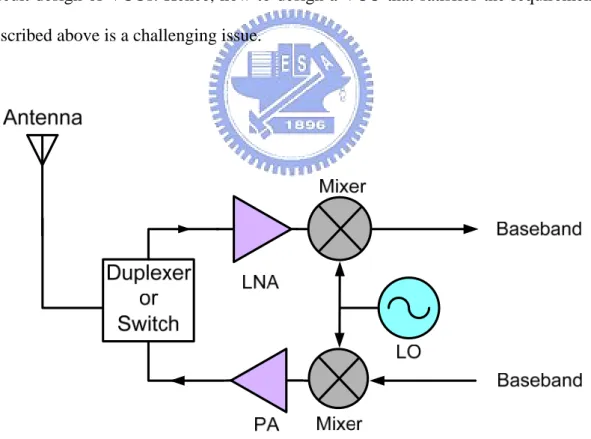
Among function blocks of a RF transceiver as shown in Figure 1.1, the voltage controlled oscillator (VCO) is used to provide clean, stable, and precise carrier signals
Chapter 1 Introduction
for frequency translation in wireless transceivers. Because the purity (phase noise) of local signal which generated by the VCO will dominate the performance of the system, the design of high performance VCO is an urgent and momentous subject. In the design of VCOs, there are several common goals, such as low phase noise, low power consumption, low cost, satisfactory output power, and sufficient tuning range. Mostly, the low phase noise is a critical specification of VCOs for actual practice. As the shrinking of chip size and the growing demand of portable applications and power-efficient issues, the low voltage and low power design is another important target of VCOs. However, according to the well-known Leeson’s model of phase noise [2], the phase noise and power consumption usually formed a key tradeoff in the circuit design of VCOs. Hence, how to design a VCO that satisfies the requirements described above is a challenging issue.
Chapter 1 Introduction
1.2 Related Works and Motivation
In nowadays, the digital and baseband circuits can be implemented in CMOS process. However, the analog and RF integrated circuits are still need the special processes to accomplish. In the RFICs, due to the crucial function in wireless transceivers and power-aware demand, the development of high performance, low power and low cost VCO is an urgent demand. For CMOS process, due to the substrate loss of bulk is avoidless in silicon based technology, the Q factor of on-chip inductors and capacitors have restricted improvement to the phase noise performance in a VCO [3]. In order to achieve low phase noise in a VCO, the complementary NMOS-PMOS cross-coupled pair architecture is employed to ease the phase noise for the reasons of the tank amplitude is twice that of NMOS or PMOS only topologies and the complementary one has more symmetry output waveform [4]. But the supply voltage can not be reduced due to the much more transistors are stacked in the topology. [5] uses a harmonic tuned (HT) method to suppress the harmonic frequency of the circuit by adding an external circuit. This method can reduce the phase noise effectively, but it also increases both the chip area and power consumption.
In low power topics, reducing supply voltage is an effective method, but mostly, the supply voltage is restricted by the threshold voltage of MOS transistors. Moreover, once the supply voltage is reduced, the signal amplitude of LC-tank will be limited in turn, further decreases the signal-to-noise ratio (SNR) and increases the phase noise of VCO. In [6-7], the current-reuse method may be an effective method to reduce the power consumption, but the phase noise performance is affected by the asymmetric structure. In conclusion, how to obtain a comparable phase noise effectively at the low power level becomes a bottleneck to design.
Chapter 1 Introduction
GHz LC-VCO by the negative conductance enhancement and common mode noise reduction methods in a conventional NMOS cross-coupled VCO. In the VCO design, achieving the goal of low power or low voltage may not be a difficulty. The real problem is the phase noise performance is considerably poor at low power level. On the other hand, the bottleneck is how to improve the phase noise of VCOs at low voltage or low power operation. The negative conductance enhancement method employs an NMOS pair paralleled the LC-tank, the parasitic capacitances of the NMOS pair will increase the negative conductance of the VCO. In the analysis of Q factor, the raise of negative conductance will degrade the phase noise effectively. The common mode noise reduction method uses the contrary placement of NMOS pair and varactors and then the VCO’s gain can be reduced. Ultimately, the phase noise is reduced. Once the phase noise is degraded, the supply voltage can be reduced and is near to the threshold voltage of MOS transistors. Finally, the low power consumption can be achieved.
1.3 Thesis Organization
There are five chapters of the thesis. Chapter 2 deals with the basic concepts and parameters of VCOs. In chapter 3, some advanced popular VCO topologies are reviewed. In chapter 4, we proposed a design of low voltage and low power consumption CMOS LC VCO with the simulated and measured results. Chapter 5 conclusion is drawn.
Chapter 2 Design Basics of CMOS LC VCO
Chapter 2
Design Basics of CMOS VCO
2.1 Fundamental Characteristics of LC VCO
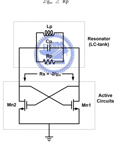
In general, the VCO is a spontaneous circuit which starts up by inherent noise and retains a stable oscillation by positive feed back and negative resistance. The VCO is used as a local oscillator that generates a precise periodic waveform for frequency up and down translation in mixer. In the analysis of VCOs, the negative resistance model (one-port network) is widely used. As shown in Figure 2.1, the oscillator is treated as two parts that one is an active circuit part and the other is resonant circuit part.
Chapter 2 Design Basics of CMOS LC VCO
When the resonator or a LC-tank resonates at a target frequency, an existed loss, represented by an equivalent resistance Rp (mostly comes from the inductor), reduces the oscillated amplitude and results in operation stop. Therefore, the active circuit provides an equivalent negative resistance -Rs to compensate the energy loss. As shown in Figure 2.2, the negative resistance -2/gm needs to satisfy the condition that
2/g
m≧ Rp
(2-1)Chapter 2 Design Basics of CMOS LC VCO
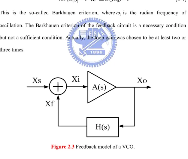
The feedback model (one-port network) is also a popular method and is widely used in the oscillator analysis. Figure 2.3 shows the block diagram of the feedback model. The transfer function of the output/input is given as
( ) ( )
( ) 1 ( ) ( )
Xo s A s
Xs s = −A s H s (2-2)
where is complex frequency. The oscillation will keep in certain amplitude if the open loop gain
s
( )
( ) ( )
Ao s
=
A s H s
(2-3) with
Ao
( ) 1
ω
0=
&
∠
Ao j
(
ω
0)
=
0
(2-4) This is the so-called Barkhauen criterion, whereω0 is the radian frequency of oscillation. The Barkhauen criterion of the feedback circuit is a necessary condition but not a sufficient condition. Actually, the loop gain was chosen to be at least two or three times.Chapter 2 Design Basics of CMOS LC VCO
2.2 LC Tank
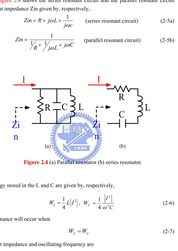
Figure 2.4 shows the series resonant circuit and the parallel resonant circuit with input impedance Zin given by, respectively,
1 Zin R j L
j c ω
ω
= + + (series resonant circuit) (2-5a) 1 1 1 Zin j C R j L
ω
ω
=+ + (parallel resonant circuit) (2-5b)
Figure 2.4 (a) Parallel resonator (b) series resonator.
The energy stored in the L and C are given by, respectively, 1 2 4 L W = L I , 2 2 1 4 C I W C ω = (2-6) The resonance will occur when
WL =WC (2-7) he input impedance and oscillating frequency are
T
Zin R
=
(2-8) 0 1 LCω ω
= = (2-9)Chapter 2 Design Basics of CMOS LC VCO
From the analysis of LC-tank, the Q (quality) factor is given as
average enegy store Q
average energy loss per cycle
ω
= (2-10)
Therefore the Q factor of the resonant circuit is 0 0 1 L Q R RC ω ω
= = (series resonant circuit) (2-11a)
0 0 R Q L ω ω
= = RC (parallel resonant circuit) (2-11b)
2.3 Phase Noise
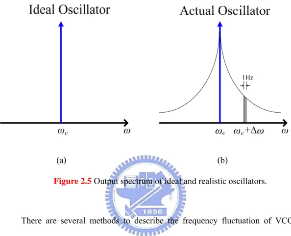
One of the most important characteristic of VCOs is phase noise which represents the purity and stability of the output signal of a VCO. The signal to noise ratio (SNR) is also affected by phase noise greatly in a transceiver. In light of ideal case, the output spectrum of an oscillator has only one impulse at the fundamental frequency as shown in Figure 2.5(a). In practice, however, the output spectrum of an oscillator is not so clear due to the spurious signals come from its harmonics or intermodulation products. Then the noise skirts which spread the fundamental output tone at oscillated frequency in a VCO, as shown in Figure 2.5(b).
An ideal sinusoidal wave form is defined as
0
( ) cos( )
V t = A ωt+ (2-12) φ where A is the oscillated amplitude, ω0 is oscillated frequency and φ is a random phase. The waveform function should be
V t( )= A t f( ) (
ω
0t+φ
( ))t (2-13)where the oscillated amplitude A t( ) and phase φ( )t are functions of time t, the function f has the period of 2π . The jitter can cause the amplitude fluctuation and phase fluctuation in a VCO. Mostly, the amplitude fluctuation can be neglected due to
Chapter 2 Design Basics of CMOS LC VCO
the voltage limiter or nonlinearity effect of the circuits, but the phase fluctuation can not.
Figure 2.5 Output spectrum of ideal and realistic oscillators.
There are several methods to describe the frequency fluctuation of VCOs. Here, we briefly present some works about phase noise model, one is D. B. Leeson and the other is A. Hajimiri.
2.3.1 Leeson’s Model
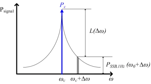
As the empirical method, the phase noise of signals is usually expressed in the description that relative to the carrier power per Hertz of bandwidth (dBc/Hz). The phase noise is typical expressed as [2]
( )
10log SSB Hz,1(
0) (
C P L d Pω
ω
ω
⎡ + Δ ⎤ Δ = ⎢ ⎥ ⎣ ⎦ Bc Hz)
(2-14) whereΔω is the offset frequency form the carrier frequency, PSSB Hz,1(
ω0+ Δω)
Chapter 2 Design Basics of CMOS LC VCO
represents the single sideband (SSB) power at a frequency offset ofω0+ Δ from the ω carrier with a measurement bandwidth of 1Hz, and PC is the carrier power, as shown
in Figure 2.6.
Figure 2.6 The diagram of the oscillator power spectrum around the fundamental.
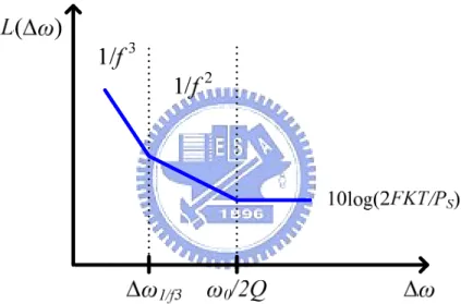
In 1966, D. B. Leeson proposed a model to describe the phase noise, this model is expressed as [2],
( )
3 2 1 0 2 10 log 1 1 2 f S L FKT L P Q ω ω ω ω ω ⎧ ⎡ ⎛ ⎞ ⎤ ⎛ Δ ⎞⎫ ⎪ ⎢ ⎥ ⎪ Δ = ⎨ ⋅ +⎜ Δ ⎟ ⋅ +⎜⎜ Δ ⎟⎟⎬ ⎢ ⎝ ⎠ ⎥ ⎪ ⎣ ⎦ ⎝ ⎠⎪ ⎩ ⎭ (2-14) where F is the excess noise factor, K is the Boltamann’s constant, T is the absolute temperature, PS is the average power consumption of resonator, ω0 is the oscillatorfrequency, QL is the loaded Q, and
Δ
ω
1 f3 is the corner frequency. Figure 2.6 doesnot express the actual shape of a SSB spectrum for a VCO, the actual SSB phase noise often approximate to the diagram shown in Figure 2.7, which shows the typical regions of phase noise of VCOs from the Lesson’s phase noise model. According to
Figure 2.7, the corner frequency
Δ
ω
1 f3 of 1 f phase noise should be equaled to 3Chapter 2 Design Basics of CMOS LC VCO
experimental steps, the
Δ
ω
1 f3 is not equal to theΔ
ω
1 f in an actual oscillator. The 31 f
ω
Δ
is a kind of empirical result without any physics significance. The power spectral density of flicker noise of active devices (MOS) is proportional to 1 f . This results in the 1 f region and closes the oscillated frequency. 3From equation (2-14), increasing the Q factor of a LC-tank and PS can
improve phase noise effectively, but the Q factor and PS are usually restricted by the
poor-Q inductor in CMOS process and low power applications respectively.
Figure 2.7 Phase noise curve of Lesson’s model.
Leeson’s phase noise model includes an empirical factor F in the description. Therefore it can not analyze the phase noise of a VCO precisely. A more accurate model is proposed by Hajimiri and T. Lee in 1998 [8].
Chapter 2 Design Basics of CMOS LC VCO
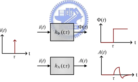
2.3.2 Hajimiri Model
The Hajimiri model introduces impulse sensitivity function (ISF) to analyze the phase noise. This model can explain the mechanisms that how the flicker noise upconvert to phase noise in a VCO. An oscillator can be modeled as a system with n noise source inputs and two outputs that are the instantaneous amplitude and excess phase of an oscillator. Noise inputs to the system are in the form of current sources injecting into circuit nodes and voltage sources in series with circuit branches. For each noise input source, both systems can be considered as single-input, single-output systems. Then the time and frequency-domain fluctuations of and
can be characterized as the two equivalent systems shown in Figure 2.8. ( ) A t ( ) A t ( )t Φ ( )t Φ
Figure 2.8 Phase and amplitude impulse response model.
A time varying impulse response can be written as [8]
( )
( ) (
0 max , h t u t qω τ
)
τ
τ
Φ Γ = − (2-15) where qmax is the maximum charge displacement across the capacitor and u(t) is theChapter 2 Design Basics of CMOS LC VCO
unit step, τ is the time when the impulse is injected and Γ
( )
x is the impulse sensitivity function (ISF). Using the relevant Fourier series, then the Γ(
ω τ0)
can be expanded as( )
0(
0 1 cos 2 n n C C n 0 n)
ω τ ∞ = Γ = +∑
ω τ θ (2-16) +where the coefficients Cn are real and θn is the phase of nth harmonic of the ISF.
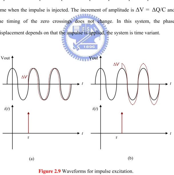
The phase noise depends on the time when the noise current is injected. In
Figure 2.9 (a), the impulse at the zero crossing causes phase noise only and does not cause amplitude noise. As shown in Figure 2.9 (b), the impulse as the peak causes amplitude noise only. The amplitude of impulse response of phase depends on the time when the impulse is injected. The increment of amplitude is
ΔV = ΔQ/C
and the timing of the zero crossings does not change. In this system, the phase displacement depends on that the impulse is applied, the system is time variant.t Vout t τ i(t) ∆V t Vout t τ i(t) ∆V (a) (b)
Chapter 2 Design Basics of CMOS LC VCO
For a given impulse sensitivity function oscillator, the excess phase due to the noise current can be obtained
( )
( ) ( )
1( ) ( )
0 max 1 , t h t i t d i t q dτ
τ
ω τ
∞ Φ −∞ −∞ Φ =∫
⋅ =∫
Γ ⋅τ
(2-17)where the coefficients Cn are real and θn is the initial phase of nth harmonic of the
ISF, qmax = CVmax, Vmax is the largest amplitude of the VCO. If the oscillator take
account of white noise 2
n
i Δ , then the SSB phase noise is f
( )
i2 2 f 2 2 max 10log 2 n rms L qω
ω
⎛ Δ Γ ⎞ Δ ≈ ⎜⎜ ⋅ ⎟⎟ Δ ⎝ ⎠ (2-18) and the SSB phase noise due to flicker noise is
( )
2 2 1 0 2 2 max10log
8
f ni
f C
L
q
ω
ω
ω
ω
⎞
Δ
≈
⎜
⎜
⋅
⎟
⎟
Δ
Δ
⎝
⎠
(2-19) To general belief, the phase noise 1/f 3 is identical to the flicker noise 1/f. The equation⎛
Δ
(2-19) indicates that the 1/f 3 region can be reduced once the Fourier coefficient C0 is
diminished. On the other hand, the meaning of diminished C0 is the more symmetrical
output waveform is achieved in a VCO. The Hajimiri model provides the exhaustive analysis on phase noise. This model can help the designer to understand the noises from each source and how they affect the phase noise. Finally, the designer can suppress the phase noise in an efficient way.
Chapter 3 Advanced Design of Related Works
Chapter 3
Advanced Design of Related Works
3.1 Basic CMOS LC VCO Topologies
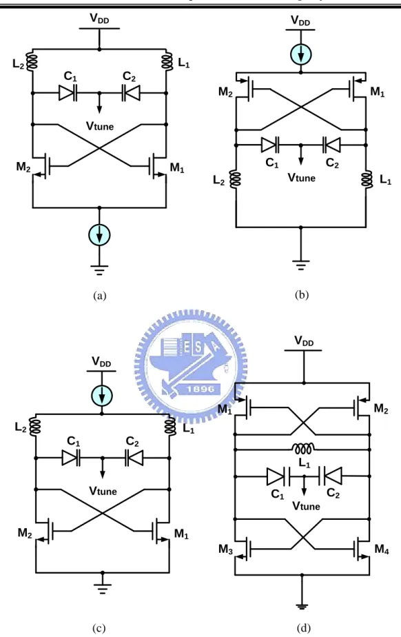
Figure 3.1 (a)-(d) show the prototypes of conventional CMOS LC VCOs published in [2], [8-10]. Topologies in Figure 3.1 (a) with a tail current source and in
Figure 3.1 (b)-(c) with top current sources have the advantage of less supply voltage due to less stages are stacked in vertical. Because they are not all control by the DC bias once the current sources are employed in Figure 3.1 (a)-(c), the VCOs could reduce the sensitivity of the proposed circuit gain versus the supply voltage effectively. But, it means that the more supply voltage may be needed. Furthermore, the current sources will down convert the noise around 2 f by channel length modulation to the 0 phase noise and degrades the phase noise.
Because of the flicker noise performance in PMOS is better than that in NMOS, the cross-coupled PMOS LC VCO were usually employed as the active circuit as shown in figure 3.1 (b). The difference between Figure 3.1 (a) and Figure 3.1 (c) is that the output DC level is close to supply voltage and close to ground respectively.
Chapter 3 Advanced Design of Related Works Vtune M1 M2 L2 L1 Vtune VDD M1 M2 L2 L1 C1 C1 C2 C2 (a) (b) VDD M3 M4 Vtune M1 M2 VDD L1 C1 C2 (c) (d) Vtune M1 M2 L2 C1 C2 VDD L1
Figure 3.1 (a) NMOS cross-coupled LC VCO with a bottom current source. (b) PMOS cross-coupled LC VCO with a top current source. (c) NMOS cross-coupled LC VCO with a top current source. (d) Complementary cross-coupled LC VCO.
Chapter 3 Advanced Design of Related Works
In Figure 3.1 (d), the complementary LC VCO not only has the more symmetric topology which could suppress the 1 f noise up-conversion by its symmetric waveforms but also generates the output waveforms which are twice of that in NMOS or PMOS only architectures, therefore the complementary architecture has the better phase noise performance. However, comparing to another topologies in
Figure 3.1, the complementary one consumes more voltage headroom and the larger size of transistors are needed to get enough transconductance to loose the overdrive voltage at low voltage operation, which results the increase of parasitic capacitance and decrease of tuning range. The LC VCOs in Figure 3.1 (a-c) have the related larger voltage headroom, the wider tuning range and the smaller size of transistors to start the oscillation than that in Figure 3.1 (d). But the cost is that the AM −FM conversion from the current source reducing the phase noise performance.
Figure 3.2 shows the LC VCO of two differential frequency tuning tanks
[11-12]. Four varactors are used for frequency tuning instead of two varactors which are employed in conventional design. When using varactors with the contrary polarities, the common mode voltage for V+ and V- are cancelled out. The varactors in Figure 3.2 are accumulation mode MOS varactors [13]. Tuning of all LC-tank oscillators may be achieved by tuning its effective capacitance with an appropriate bias control voltage (V+ and V-). Since CMOS junction capacitors have relatively poor Q, it is advisable to use as much junction capacitance as necessary to achieve the desired tuning range.
Chapter 3 Advanced Design of Related Works
Figure 3.2 Schematic of two differential frequency tuning LC VCO.
3.2 Related CMOS LC VCO Issues
In the past research, effort to reduce phase noise has been published in several methods, one of that is to reduce phase noise of the LC-VCO by adding external circuits and enhancing the quality factor (Q) [14]. In this method, the tail current is made large when the oscillator output voltage reaches its peak value and when the sensitivity of the output phase to injected noise is the smallest; the tail current is made small during the zero crossings of the output voltage when the phase noise sensitivity is large. But, this method consumes more voltage headroom and power consumption
Chapter 3 Advanced Design of Related Works
due to its tail current source. As shown in Figure 3.3 which proposes a harmonic tuned (HT) method that suppresses the harmonic frequency of the circuit by opening the fundamental and third frequencies and shortening the second harmonic by inserting L2, L3, C3 and C4 as a harmonic tuning network [5]. This method can reduce
the phase noise effectively but the drawbacks are to increase the chip area and power consumption.
Figure 3.3 Schematic of simplified HT CMOS LC VCO
Chapter 3 Advanced Design of Related Works
Figure 3.4 shows the full PMOS LC VCO with a top current source [15]. In most cases, the major noise contributor in VCOs is the channel noise form CMOS transistors [16]. In this condition, the use of PMOS is more attractive since the PMOS transistors have lower 1 f noise than that in NMOS transistors [3], [17]. Furthermore, the large capacitor CE parallels the current source is needed because of
the transistors of the differential pair might carry very little current for a fraction of the cycle. Thus, the duty cycle of the drain current waveform is reduced significantly. As a result, the drain current noise injection during the zero-crossing of the tank differential voltage can be reduced and the better phase noise performance is achieved. In addition, the CE attenuates both the high-frequency noise components of the tail
current and the voltage variations on the tail node. The improvement of voltage variations results in more symmetric waveforms and smaller harmonic distortion in VCO outputs.
Chapter 3 Advanced Design of Related Works
It is well known that the higher quality factor can be achieved by exciting an inductor differentially rather than single ended [18]. Therefore, as shown in Figure 3.4, the use of a symmetric center-tapped inductor not only has the more symmetric output waveforms of the LC-tank but also has the benefits of the coupling factor to increase the inductance value and can lead to save the chip area.
In the design of low power CMOS LC VCO, current-reused is a method in common use [6-7], [19]. Figure 3.5 shows the schematic of the current-reused CMOS LC VCO. The current-reused LC-VCO uses both NMOS and PMOS transistor in cross-coupled pair as a negative conductance generator to achieve low power consumption easily. The series stacking of NMOS and PMOS allows the supply current to be reduced by half compared to that of the conventional LC-VCO while providing the same negative conductance. This topology is not only low power consumption but also low cost since it used only one inductor and two MOS transistors..
Chapter 3 Advanced Design of Related Works
Another method for a VCO to operate in low power consumption is the transformer feedback (TF) structure [20]. As shown in Figure 3.6, the drain and source voltages are decreased when the gate voltage is increased simultaneously. The reduction of the source voltage lowers the ground potential effectively and allows the drain voltage to sweep to a negative potential before the transistor gets into the linear region. As a result, the phase synchronization provides extra voltage headroom for the drain oscillation, the drain voltage could swing above the supply voltage and the source voltage could swing below the ground level. Furthermore, the drain and source signals oscillate in phase. Substantially, the oscillation amplitude is enhanced, and consequently, the supply voltage can be reduced for the same phase noise with lower power consumption. In Figure 3.6, the TF VCO uses a single transformer for the feedback across the drain and source terminals, which structure is similar to the Hartley design [21-23].
Chapter 4 Design of a Fully Integrated Low Voltage Low Power CMOS LC VCO
Chapter 4 Design of a Fully Integrated Low
Voltage Low Power CMOS LC VCO
4.1 Introduction
As the modern CMOS process technology has been scaled down and the market trend moves toward a greater scale of integration gradually, the reduction of power consumption has become considerably important to portable devices in the applications of wireless communication system. As we can see in Table 4.1, weather the RF technology or the analog and mixed signal technologies, all the supply voltage are forced to reduce by the shrink of process technology [24].
In general, the most direct and efficient way to reduce power consumption in circuit design is to reduce the supply voltage. However, the supply voltage is relies on the threshold voltage chiefly. Once the supply voltage can be reduce, the MOS transistors may go into subthreshold regime, this result will bring about the decrease of reliability. Furthermore, unfortunately, the low supply voltage is usually limits the output signal amplitude, which leads to degrades the signal to noise ratio and deteriorates the phase noise performance in turn.
Chapter 4 Design of a Fully Integrated Low Voltage Low Power CMOS LC VCO
TABLE 4.1
ANALOG, MIXED SIGNAL, AND RF TECHNOLOGY ADVANCE TREND.
Year 1997 250nm 1999 180nm 2001 150nm 2003 130nm 2006 100nm 2009 70nm 2012 50nm Supply voltage (V) 2.5-1.8 1.8-1.5 1.6-1.3 1.5-1.2 1.2-0.9 0.9-0.6 0.8-0.5 Frequency (GHz) 1.8-2.5 2.5-3.5 3.0-4.0 3.5-5.0 5.0-6.5 6.5-9.5 9.5-13
In this chapter, we propose the design of low voltage and low power consumption CMOS LC-VCO with negative conductance enhancement and common mode noise reduction method. The section 4.2 briefly describes the low voltage LC VCO topology that can operate with less voltage headroom compared to complementary LC VCO topology due to less transistors are stacked in vertical direction. In the section 4.3, the low voltage LC-VCO with negative conductance enhancement method and common mode noise rejection is proposed. Comparing to conventional LC VCO, the simulated results are illustrated in section 4.4. In section 4.5, the measured results are shown.
Chapter 4 Design of a Fully Integrated Low Voltage Low Power CMOS LC VCO
4.2 Low Voltage and Low Power LC VCO
In the design of LC VCO in low voltage operation, it mostly restricted by the threshold voltage of MOS transistors. However, as the advancement of CMOS process technology continue increasing, the threshold voltage of MOS transistors can be reduced to milivoltage level. It is a good deal for the design of low supply voltage LC VCOs. However according to the Leeson model of phase noise, we can see that there have two ways to improve the phase noise performance, one is to increase Q factor and another is to increase the average power in the LC-tank. Due to the serious loss of inductor in CMOS process technology, the first method mostly dominated by inductor which has the poor Q factor than varactors. The later method means that the more power consumption (or supply voltage) is needed. In the consideration of power-saving, this method is not efficient enough. Therefore, how to design a low voltage, low power consumption LC VCO and maintain comparable phase noise level is a difficult problem.
Figure 4.1 shows the conventional design of low supply voltage LC VCO. The LC-VCO consists of two deferential symmetrical inductors (L1 and L2), two accumulation-mode MOS varactors (C1 and C2) and a MIM capacitor (C3). The NMOS cross-coupled pair (M1 and M2) serves as the negative resistance to compensate for the energy losses from the LC-tank. The C3, L1 and L2 set the fix frequency while the C1 and C2 with the control voltage make the frequency tunable. The circuit has a symmetric topology to create symmetric output waveforms, which can reduce l/f noise up-conversion [25]. By the optimal design in the conventional LC VCO, we got the simulated results as shown in Figure 4.2 (a)-(b). In Figure 4.2 (a) the phase noise is -112.66 from 1MHz offset frequency at 3.4 GHz with 0.5V supply voltage and 0.54 mW power consumption. In Figure 4.2 (b) the tuning range
Chapter 4 Design of a Fully Integrated Low Voltage Low Power CMOS LC VCO
with 0 to 0.5 V control voltage is drawn.
Figure 4.1 Conventional CMOS LC VCO with NMOS cross coupled pair.
0.2 0.4 0.6 0.8 0.0 1.0 -100 -80 -60 -40 -120 -20 Offset Frequency (MHz) P has e N oi se (d B c/ H z)
Chapter 4 Design of a Fully Integrated Low Voltage Low Power CMOS LC VCO 0.1 0.2 0.3 0.4 0.0 0.5 3.30 3.32 3.34 3.36 3.38 3.40 3.28 3.42 Control Voltage (V) O sc illa te d F requenc y (G H z)
Figure 4.2 (b) The simulated tuning range of the conventional NMOS only LC VCO.
As we can see in Figure 4.2 (a),the low supply voltage can be achieved due to the less transistors are stacked. But the phase noise is usually not satisfied. Here, we proposed a negative conductance enhancement and common mode noise rejection method to improve the phase noise.
4.3 Design and Analysis of the Proposed LC VCO
4.3.1 Negative Conductance Enhancement
In the analysis of Q factor of a LC tank, the relation between conductance and Q factor is (4-1)
1
PC
Q
G
L
=
where the Gp is the conductance of a LC tank, the diagram of a LC tank with negative conductance is shown in Figure 4.3.
Chapter 4 Design of a Fully Integrated Low Voltage Low Power CMOS LC VCO
As the equation (4-1), we can obtain the result that Q factor will be increase when the GP is decrease. Therefore, as shown in Figure 4.4, if we could add an
additional negative conductance -GN to the LC tank, the total conductance Gtot will be
degraded.
L
C
G
P
Figure 4.3 An LC tank with conductance.
Figure 4.4 An LC tank with negative conductance.
According to [26], the negative conductance can be obtained from the topology in Figure 4.5, and the value of negative conductanceis
(4-2) 2
(
)
gs N gd N mC C
C
G
g
ω
+
=
M
NC
NChapter 4 Design of a Fully Integrated Low Voltage Low Power CMOS LC VCO
With the negative conductance is presented above, we now take this method into the proposed LC VCO to enhance the negative conductance. Figure 4.6 shows the proposed LC VCO with an NMOS pair, M3 and M4 that in parallel to conventional NMOS only cross-coupled LC VCO. For the demand of measurement, the M5 and M6 are served as buffer stages.
Figure 4.6 The proposed low voltage, low power consumption CMOS LC VCO.
Chapter 4 Design of a Fully Integrated Low Voltage Low Power CMOS LC VCO
Figure 4.7 shows the parasitic capacitances Cgs and Cgd of the proposed LC VCO. Due to the differential topology of the LC VCO, the equivalent circuit in Figure 4.7 can be equal to Figure 4.8. As shown in Figure 4.9, the parasitic capacitances Cgs3,
Cgd3 of M3, and Cgs4, Cgd4 of M4 provide an additional negative conductance with M1
and M2. According to equation (4-2), the total negative conductance of the proposed LC VCO is (4-3) 2 2 1 3 3 1 2 4 4 2 1 2
(
)
(
)
gs gd gs gd gs gd gs gd N m mC
C
C
C
C
C
C
C
G
g
g
ω
⎡
⎣
+
+
⎤
⎦
ω
⎡
⎣
+
+
=
+
⎤⎦
Chapter 4 Design of a Fully Integrated Low Voltage Low Power CMOS LC VCO
Figure 4.8 The parasitic capacitances of M3 and M4 of the proposed LC VCO.
Figure 4.9 Negative conductance of the proposed LC VCO.
However, in order to avoid the cease of oscillation, the additional negative conductance should not be large than the conductance of LC tank.
Chapter 4 Design of a Fully Integrated Low Voltage Low Power CMOS LC VCO
4.3.2 Common Mode Noise Reduction
Common mode noise is an unwanted noise, which upconvert to the carrier frequency and result serious jitter and weak phase noise performance in LC VCOs. For this reason, we employ a common mode noise reduction method to suppress the common mode noise [11-12]. Figure 4.10 shows the common mode noise rejection of the proposed LC VCO.
Figure 4.10 Common mode noise reduction of the proposed LC VCO diagram.
The common mode voltage Vcm is
T
(
m)
I
Vcm V
g
≅
+
(4-4)Chapter 4 Design of a Fully Integrated Low Voltage Low Power CMOS LC VCO
where I is the total current in the VCO, VT and gm are the threshold voltage and transconductance of the NMOS respectively. The -△Vgb and +△Vgb are the gate to bulk terminal voltage of the proposed NMOS pair (M3 and M4) and varactors (C1 and C2) respectively. In order to reduce the common mode noise, the symmetry of differential tuning is needed. According to mathematical analysis, the capacitances of NMOS pair and varactors can be shown as
0 1
(-
)
N vC
=
C
+
k
Δ
Vgb Vncm
+
(4-5a) 0 2(
V vC
=
C
−
k
+Δ
Vgb Vncm
+
)
2 v (4-5b) Where C0 is the zero bias capacitance, the Vncm is common mode noise and the kv1and
k
v2 are the capacitor gain of NMOS pair and varactors respectively. If the perfectly selection is achieved such that1
v
k
= −
k
(4-6) then the total capacitance C is
C
=
2
C
0+
2
kv Vgb
Δ
(4-7) where C=CN+CV, △Vgb =+△Vgb –(-△Vgb). In equation (4-7), the common noise iscanceled out. If not, the gain of the common mode noise is
k
v1−
k
v2 (4-8) As the common mode noise rejection has been explained above, the compared results between proposed LC VCO and conventional one is presented in next section.Chapter 4 Design of a Fully Integrated Low Voltage Low Power CMOS LC VCO
4.4
Simulation Results
Figure 4.11 shows the simulated phase noise with different body bias of the NMOS pair.As we can see, the best phase noise is around 0.6 V.
0.0 0.2 0.4 0.6 0.8 -118 -117 -116 -115 -114 P hase Noise (dBc/Hz)
Body Bias Voltage (V)
Figure 4.11 Simulated phase noise versus body bias.
As shown in Figure 4.12, the conventional and proposed LC VCOs are compared. 0.0 200.0k 400.0k 600.0k 800.0k 1.0M -120 -100 -80 -60 -40 -20 P h as e Noise ( d B c /Hz) Offset Frequnecy (MHz) conventional VC VCO proposed LC VCO
Chapter 4 Design of a Fully Integrated Low Voltage Low Power CMOS LC VCO
In the proposed LC VCO, the phase noise is -118.32 dBc/Hz at 1 MHz offset from carrier frequency. The improvement between conventional and proposed LC VCOs is about 6 dBc/Hz at 1 MHz offset frequency. Another parameter Kvco is also improved as shown in Figure 4.13.
0.05 0.10 0.15 0.20 0.25 0.30 0.35 0.40 0.45 60.0M 80.0M 100.0M 120.0M 140.0M 160.0M 180.0M 200.0M 220.0M 240.0M conventional LC VCO proposed LC VCO K v c o ( K H z /V ) Control Voltage (V)
Figure 4.13 The compared result of Kvco.
As shown in equation (4-9), the figure of merit (FOM) is widely used to compare the VCO performance among the different designs
( )
10 log 20 log 0 1 DC P FOM L mWω
ω
ω
⎛ ⎞ ⎛ = Δ + × ⎜ ⎟− × ⎜ Δ ⎝ ⎠ ⎝ ⎞ ⎟ ⎠ (4-9) where ω0 is the oscillating frequency, Δω is the offset frequency, L{ }
Δω is the phase noise at Δω, PDC is the DC power consumption of VCO in mW. The FOM ofproposed VCO are evaluated and are equal to -192 dBc/Hz.
In addition, in order to match the simulated results, the pad-effect which is provided by national chip implementation center (CIC) as shown in Figure 4.14
Chapter 4 Design of a Fully Integrated Low Voltage Low Power CMOS LC VCO
should be take into consideration. In post simulation, we finished the EM simulation by Agilent advanced design system (ADS) Momentum design tool.
Chapter 4 Design of a Fully Integrated Low Voltage Low Power CMOS LC VCO
4.5 Measured Results
In this section, the measurement results of the proposed LC-VCO are presented. In Figure 4.15 and Figure 4.16, the chip layout and microphotograph of the proposed LC-VCO are shown, respectively. The LC-VCO is fabricated in TSMC 0.18-μm 1P6M CMOS process. Its chip area including pads is 0.61×0.76 mm2.
Chapter 4 Design of a Fully Integrated Low Voltage Low Power CMOS LC VCO
Figure 4.16The Microphotograph of the proposed LC-VCO.
The LC-VCO chip was measured by on-wafer probe method. Figure 4.17
shows that the measured phase is -112.24 dBc/Hz with 0.51 V supply voltage. According to the measured current in Figure 4.18, the chip drew a total DC current is 2.05 mW. The power consumption which including buffer circuits of the LC VCO is 1.05 mW. Figure 4.19 shows the output spectrum. The measured VCO’s gain is drawn in Figure 4.20. In table 4.2, the measured results are summarized and compared with related LC VCOs.
Chapter 4 Design of a Fully Integrated Low Voltage Low Power CMOS LC VCO
Fig. 4.17 Measured phase noise of the proposed LC VCO.
Chapter 4 Design of a Fully Integrated Low Voltage Low Power CMOS LC VCO
Fig. 4.19 Output spectrum of the proposed LC VCO.
Chapter 4 Design of a Fully Integrated Low Voltage Low Power CMOS LC VCO
TABLE 4.2
COMPARED THE PROPOSED LC VCO WITH RECENTLY PUBLISHED LC VCOS
Ref. Tech. (um) fo (GHz) PN (dBc/Hz) VDD (V) PDC (mW) FoM (dBc/Hz) This work 0.18 CMOS 3.3 -112.2 0.51 1 -182.6 [27] 0.18 CMOS 2.2 -122 1.8 18.5 -176.2 [28] 0.18 CMOS 2.4 -113 0.75 4.5 -178.8 [29] 0.18 CMOS 2 -111.7 0.9 0.5 -180.7 [30] 0.18 CMOS 3.5 -108.5 1.2 4.5 -161.6
Chapter 5 Conclusions and Future Work
Chapter 5 Conclusions
A fully integrated, low voltage and low power CMOS LC-VCO with negative conductance enhancement and common mode noise reduction is proposed and implemented by TSMC 0.18-μm 1P6M CMOS process. The design uses the conventional NMOS only cross-coupled topology combined with an NMOS pair to improve the phase noise performance in low voltage operation. The proposed LC-VCO consumes 1 mW with 0.51 V supply voltage. The measured phase noise at 1 MHz offset frequency is -112.24 dBc/Hz at 3.3GHz. Although the supply voltage and power consumption are obviously improved, there is still a lot of space for noise reduction. Several extensive studies have been underway to further reduce the phase noise of LC-VCOs. In this field, it maybe worth our effort in the future works, such as low phase noise LC-VCOs.
References
REFERENCES
[1] IEEE 802.16e/D12-2005, “IEEE Standard for Local and Metropolitan Area Networks - Part 16: Air Interface for Fixed Broadband Wireless Access Systems - Amendment for Physical and Medium Access Control Layers for Combined Fixed and Mobile Operation in Licensed Bands,” October. 2005.
[2] D. B. Lesson, “A simple model of feedback oscillator noise spectrum,” Proc. IEEE, vol. 54, pp. 329-330. Feb. 1966.
[3] Yi Lin, K.H. To, J. S. Hamel, and W. M. Huang “Fully Integrated 5GHz CMOS VCOs with On Chip Low Frequency Feedback Circuit for 1/f Induced Phase Noise Suppression,” Solid-State Circuits Conference, pp. 551-554, Sept 2002. [4] Jishnu, Bhattacharjee, Debanjan Mukherjee, Edward Gebara, Sebastien Nuttinck
and Joy Laskar, “A 5.8 GHz Fully Integrated Low Power Low Phase Noise CMOS LC VCO for WLAN Applications,” 2002 IEEE MTT-S Digest, pp. 585-588, 2002.
[5] Hjijung Kim, Seonghan Ryu, Yujin Chung, Jinsung Choi, and Bumman Kim, “A low phase noise CMOS VCO with harmonic tuned LC tank,” IEEE Trans. Microw. Theory Tech., vol. 54, no. 7, pp. 2917-2924, July 2006.
[6] N. J. Oh and S. G. Lee, “Current reused LC VCOs,” IEEE Microw. Wireless Compon. Lett., vol. 15, no. 11, pp. 736–738, Oct. 2005.
[7] Y.-H. Chuang, S.-L. Jang, S.-H. Lee, R.-H. Yen, and J.-J. Jhao, “5-GHz Low Power Current-Reused Balanced CMOS Differential Armstrong VCOs,” IEEE Microw. Wireless Compon. Lett., vol. 17, no. 2, pp. 139–141, Feb. 2007.
[8] A. Hajimiri and T. H. Lee, “A general theory of phase noise in electrical oscillator,” IEEE J. Solid-State Circuits, vol.33, pp. 179-194, Feb. 1998.
References
[9] B. Razavi, "RF Microelectronics," Upper Saddle River, NJ: Prentice Hall, 1997. [10] A. Hajimiri, T. Lee, "Design Issues in CMOS Differential LC Oscillators," IEEE
J. Solid-State Circuits, vol. 34, pp. 717-724, May 1999.
[11] N. H. W. Fong, J. O. Plouchart, N. Zamdmer, D. Liu, L. F.Wagner, and N. G. Tarr, “A 1-V 3.8–5.7-GHz wide-band VCO with differentially tuned accumulation MOS varactors for common-mode noise rejection in CMOS SOI technology,” IEEE Trans. Microw. Theory Tech., vol. 51, no. 8, pp. 1952–1959, Aug. 2003.
[12] H. Moon, S. Kang, Y. T. Kim, and K. Lee, “A fully differential LC-VCO using a new varactor control structure,” IEEE Microw. Wireless Compon. Lett., vol. 14, no. 9, pp. 410–412, Sep. 2004.
[13] Theerachet Soorapanth, C. Patrick Yue, Derek K. Shaeffer, Thomas H. Lee, and S. Simon Wong, “Analysis and optimization of accumulation-mode varactor for RFICs, ” in IEEE Symposium on VLSI Circuits Digest of Technical Papers, New York, NY, June 1998, pp. 32-33.
[14] Babk Soltanian and Peter R. Kinget, “Tail current-shaping to improve phase noise in LC voltage-controlled oscillators,” IEEE J. Solid-State Circuits, vol. 41, no. 8, pp. 1792–1802, Aug. 2006.
[15] Giuseppe De AStis, David Cordeau, Jean-Marie Paillot, and Lucian Dascalescu, “A 5-GHz fully integrated full PMOS low-phase-noise LC-VCO,” IEEE J. Solid-State Circuits, vol. 40, no. 10, pp. 2087–2091, Oct. 2005.
[16] M. A. Margarit, J. L. Julian Tham, R. G. Meyer, and M. J. Deen, “A low noise, low-power VCO with automatic amplitude control for wireless applications,” IEEE J. Solid-State Circuits, vol. 34, no. 6, pp. 761–771, Jun. 1999.
[17] K. O. Kenneth, N. Park, and D. J. Yang, “1/f noise of nMOS and pMOS transistors and their implications to design of voltage controlled oscillators,” in
References
IEEE Radio Frequency Integrated Circuit Symp. Dig., Jun. 2002, pp. 59–62. [18] M. Danesh, J. R. Long, R. A. Hadaway, and D. L. Harame, “A Q-factor
enhancement technique for MMIC inductors,” in IEEE Int. Microwave Symp. Dig., vol. 1, Jun. 1998, pp. 183–186.
[19] S. Yun, S. Shin, H, Chol, S. Lee, "A 1 nW Current-Resue CMOS Differential LC-VCO with Low Phase Noise," IEEE International Solid-State Circuits Conf., pp. 540-542, Feb. 2005.
[20] KaChun Kwok and Howard C. Luong, “Ultra-Low-Voltage High-Performance CMOS VCOs Using Transformer Feedback,” IEEE J. Solid-State Circuits, vol. 40, no. 3, pp. 1018–1024, Jul. 2001.
[21] R. Hartley, “Oscillation generator,” U.S. Patent 1,356,763, Oct. 26, 1920. [22] B. Razavi, Design of Analog CMOS Integrated Circuits. Boston, MA: McGraw
-Hill, 2001.
[23] Shao-Hua Lee, Yun Hsueh Chuang, Sheng-Lyang Jang, and Chien-Cheng Chen, ”Low-phase noise Hartley differential CMOS voltage controlled oscillator,” IEEE Microw. Wirelsess Compon. Lett., vol. 17, no. 2, pp. 145-147, Feb. 2007.
[24] The International Technology Roadmap for Semiconductors.
[25] T.H. Lee, and A. Hajimiri, "Oscillator phase noise: a tutorial," IEEE Journal of Solid State Circuits, vol. 35, 1103, pp.326-336, March 2000.
[26] M.A. Do, R. Zhao, K.S. Yeo, J.G. Ma, ”1.5V 1.8GHz bandpass amplifier,” in IEEE Proceedings-Circuits, Devices and System, vol. 147, no. 321-33, Dec. 2000.
[27] Seok-Ju Yun, Chong-Yul Cha, Hyoung-Chul choi, and Sang-Gug Lee, “RF CMOS LC-oscillator with source damping resistors,” IEEE Trans. Microw. Wireless Compon. Lett., vol. 16, pp. 511-513, Sep. 2006.
References
[28] Y.-H. Chuang, S.-H. Lee, R.-H. Yen, S.-L. Jang, J.-F. Lee, and M.-H. Juang, “A wide locking range and low voltage CMOS direct injectionlocked frequency divider,” IEEE Microw. Wireless Compon. Lett., vol. 16, no. 5, pp. 299–301, May 2006.
[29] H. Lee, T. Choi, S. Mohammadi, and L. P. B. Katehi, “An extremely low power 2 GHz CMOS LC VCO for wireless communication applications,” in Proc. IEEE Eur. Conf. Wireless Technol., Paris, France, Oct. 2005, pp. 41–44.
[30] M. J. Deen, R. Murji, A. Fakhr, N. Jafferali, and W. L. Ngan, “Low power CMOS integrated circuits for radio frequency applications,” IEE Proceedings on Circuits, Devices and Systems, in press.
[31] Adel S. Sedra and Kenneth C. Smith, Microelectronic Circuits, 5rd edition, Oxford. 2004.
[32] D. M. Pozar, Microwave Engineering, 3rd edition, John Wiley & Sons. 2005. [33] Bosco Leung, VLSI for wireless communication, Prentice Hall, 2002.
[34] Thomas H. Lee, The Design of CMOS Radio-Frequency Integrated circuits, Cambridge University Press, 1998.
[35] B. Razavi, Design of Analog CMOS Integrated Circuits, MCGRA-Hill, 2001.
[36] J. Craninckx and M. Steyaert, Wireless CMOS Frequency Synthesizer Design, Norwell, MA: Kluwer, 1998.
[37] J. W. M. Rogers, J. A. Macedo, and C. Plett, “The effect of varactor nonlinearity on the phase noise of completely integrated VCO,” IEEE, J. Solid-State Circuits, vol. 35, no. 9, pp. 1360-1367, Sep. 2000.
[38] Christian Enz, “An MOS transistor mode for RF IC design valid in all regions of operation,” IEEE Trans. Microw. Theory Tech., vol. 50, no. 1, pp. 342-359, Jan 2002.
References
RF IC Design,” IEEE Trans. Electron Devices, vol. 32, no. 7, pp. 1286-1303, July 2005.
[40] Aly Ismail and Asad A. Abidi, “CMOS differential LC oscillator with suppressed UP-converted flicker noise,” IEEE Int. Solid-State Circuits Conf., vol. 1, pp. 98-99, 2003.