適用於雙頻帶接收機前端電路之共電流低雜訊放大器和低電壓微混頻器
86
0
0
全文
(2) 適用於雙頻帶接收機前端電路之 共電流低雜訊放大器和低電壓微混頻器 Concurrent Dual-Band LNA For Dual-Band Receiver Front-End and Low-Voltage Micromixer. 研究生:顏欽賢. Student:Chin Hsien Yen. 指導教授:周復芳 博士. Advisor:Dr. Christina F. Jou. 國立交通大學 電信工程學系碩士班 碩 士 論 文 A Thesis Submitted to Department of Communication engineering College of Electrical Engineering and Computer Science National Chiao Tung University In Partial Fulfillment of the Requirements For the Degree of Master of Science In Communication Engineering June 2004 Hsin Chu, Taiwan, Republic of China 中 華 民 國 九 十 四 年 六 月.
(3) 適用於雙頻帶接收機前端電路之 共電流低雜訊放大器和低電壓微混頻器 Concurrent Dual-Band LNA For Dual-Band Receiver Front-End and Low-Voltage Micromixer 研究生 : 顏欽賢. 指導教授 : 周復芳 博士. 國立交通大學電信工程學系碩士班. 中文摘要 本論文的第一部份分三個方面研究共電流雙頻帶低雜訊放大器電路設計方 法,包含輸入匹配,雜訊指數,和功率消耗,並且以電路元件來表示這些特性。 實作的共電流雙頻帶低雜訊放大器顯示在 2GHz 和 5.25GHz 分別有 7.45 dB 和 6.06 dB 的增益,-12.8 dB 和-12.9 dB 的輸入返回損耗,3.54 dB 和 4.80 dB 的雜訊指數, 並且僅消耗 7.21mw 的低功率損耗。第二部份針對採用偶次諧波混頻器而只需單 一頻率合成器的新式共電流雙頻帶接收機架構實作共電流雙頻帶接收機前端電 路。此電路在 2.45GHz 和 5.25GHz 分別達到 17.2 dB 和 11.8 dB 的電壓增益,-15.9 dB 和-15.8 dB 的射頻端輸入返回損耗,及-21.0 dBm 和-15.3 dBm 的 P1dB。第三 個部份是操作在 1V 的 2.45GHz 低電壓微混頻器。此電路在 1.72mw 的低功率消 耗下有 14.9 dB 的射頻端輸入返回損耗,8.28 dB 的轉換增益,-5.63 dBm 的 P1dB 和 4.21 dBm 的 IIP3。本論文中的三顆晶片均使用標準 0.18um CMOS 製程設計和 實作,並且在國家晶片系統設中心完成量測。. I.
(4) A Study of Concurrent Dual-Band LNA For Dual-Band Receiver Front-End Student: Chin Hsien Yen. Advisor: Dr. Christina F. Jou. Institute of Communication Engineering National Chiao Tung University. Abstract In the first part of the thesis the design method of concurrent dual-band LNA topology is studied and analyzed in three respects, including input matching, noise figure, and power dissipation. These characteristics are expressed in terms of circuit elements. The implemented concurrent dual-band LNA demonstrates 7.45 dB and 6.06 dB power gain, -12.8 dB and -12.9 dB input return loss, 3.54 dB and 4.80 dB noise figure at 2GHz and 5.25Gz, respectively, with low power consumption of 7.21mw. In the second part a concurrent dual-band receiver front-end for wireless LAN 802.11a/b/g applications is implemented base on the new concurrent dual-band receiver architecture which needs only one frequency synthesizer by employing sub-harmonic mixer. It achieves 17.2 dB and 11.8 dB voltage gain, -15.9 dB and -15.8 dB RF port input return loss, -21.0 dBm and -15.3 dBm P1dB at 2.45GHz and 5.25GHz, respectively. The third part is the 2.45GHz low-voltage micromixer for 1V operation. It has 14.9 dB RF port return loss, 8.28 dB conversion voltage gain, -5.63 dBm P1dB, and 4.21 dBm IIP3 with 1.72mw low power dissipation. The three ICs in this thesis are all designed and fabricated using CMOS 0.18um process and measured in National Chip Implementation Center (CIC).. II.
(5) Acknowledgement 首先,我要感謝指導教授周復芳老師,在這兩年來的指導和關 心,讓我在碩士學業求學過程獲益良多。並且要感謝博士班鄭國華學 長的耐心教導,尤其當我遇到困難總能給我鼓勵和信心,並且指引了 我研究方向,讓研究更有目標。 還有要感謝實驗室的同學俊賢、政宏、偉誠、家良、柏達,和學 弟博揚、文明、秋榜、仕豪、政展、宏斌,有你們陪我一起渡過這兩 年的研究生生活,彼此在學業和研究各方面相互砥礪和支持,帶給了 我一段美好、難忘、也最充實的時光。 最後我要感謝我最愛的父母親和家人,在我想走的路上,一路給 我最大的支持和包容,讓我能順利地完成碩士學業。. III.
(6) Contents Chinese Abstract .........................................................................................I English Abstract....................................................................................... II Acknowledgement………………………………………………………III Contents…………………………………………………………………IV List of Tables……………………………………...………………….VI List of Figures…………………………………...…..………………VII. Chapter 1 Introduction ..............................................................................1 1.1 Motivation .......................................................................................1 1.2 Thesis Organization ...........................................................................2. Chapter 2 Concurrent Dual-Band Low-Noise Amplifier .........................3 2.1 Introduction......................................................................................3 2.2 Architecture......................................................................................4 2.3 A Review of Single-Band LNA ...........................................................6 2.3.1 Input Matching ........................................................................7 2.3.2 Noise Figure ...........................................................................8 2.3.3 Power Dissipation ....................................................................9 2.4 Analysis of Concurrent Dual-Band LNA .............................................10 2.4.1 Input Matching ......................................................................10 2.4.2 Noise Figure .........................................................................11 2.4.3 Power Dissipation ..................................................................16 2.5 Layout Considerations .....................................................................18 IV.
(7) 2.6 Measurement Considerations ............................................................20 2.7 Experimental Results and Discussions ................................................23 2.8 Comparisons ..................................................................................30. Chapter 3 Concurrent Dual-Band Receiver Front-End ..........................31 3.1 Wireless LAN Standard Review ........................................................31 3.1.1 IEEE 802.11a ........................................................................32 3.1.2 IEEE 802.11b ........................................................................33 3.1.3 IEEE 802.11g ........................................................................33 3.2 Review of Receiver Architecture .......................................................34 3.2.1 Heterodyne Architecture .........................................................35 3.2.2 Homodyne Architecture ..........................................................36 3.2.3 Low-IF Architecture ...............................................................37 3.3 Design of Concurrent Dual-Band Receiver Front-End...........................38 3.4 Experimental Results and Discussions ................................................44 3.5 Comparisons ..................................................................................53. Chapter 4 Low-Voltage Micromixer.......................................................54 4.1 Review of Basic Micromixer .......................................................................54 4.2 Low-Voltage Micromixer.............................................................................56 4.3 Layout and Measurement Considerations....................................................59 4.4 Experimental Results and Discussions ........................................................62 4.5 Comparisons ................................................................................................67. Chapter 5 Conclusion and Future Work .................................................68 5.1 Conclusion .....................................................................................68 5.2 Future Work ...................................................................................70. Reference ................................................................................................71 V.
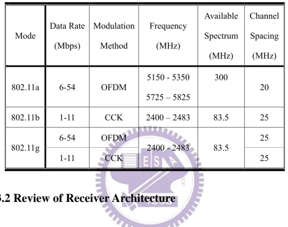
(8) List of Tables Table 2.7.1 Performance summary of concurrent dual-band LNA............................29 Table 2.8.1 Comparisons of concurrent dual-band LNA ...........................................30 Table 3.1.1 IEEE 802.11a modulation versus data rate .............................................32 Table 3.1.2 Overview of wireless LAN standard.......................................................34 Table 3.2.1 Comparisons of different receiver architectures .....................................37 Table 3.4.1 Performance summary of dual-band receiver front-end .........................48 Table 3.5.1 Comparisons of dual-band receiver front-end ........................................53 Table 4.4.1 Performance summary of low-voltage micromixer ................................66 Table 4.5.1 Comparisons of low-voltage mixers .......................................................67. VI.
(9) List of Figures Figure 2.1.1 Traditional dual-band receiver with two individual paths.......................4 Figure 2.1.2 Concurrent Dual-band receiver block diagram .......................................4 Figure 2.2.1 Schematic of the dual-band LNA ............................................................5 Figure 2.3.1 Traditional single-band low-noise amplifier ...........................................6 Figure 2.3.2 Small signal equivalent circuit of the single-band LNA .........................8 Figure 2.3.3 Small-signal equivalent circuit of single-band LNA with noise generators ................................................................................................................8 Figure 2.4.1 Small-signal equivalent circuit of dual-band LNA ...............................11 Figure 2.4.2 Small-signal equivalent circuit of dual-band LNA with noise generators ..............................................................................................................12 Figure 2.4.3 Representation of Figure 2.3.3 by two input noise generators ..............13 Figure 2.4.4 Purely parallel RLC tank .......................................................................13 Figure 2.4.5 Input equivalent series RLC model .......................................................13 Figure 2.4.6 Simulation result of noise figure under different Q1 ............................................ 16 Figure 2.4.7 Simulation result of power dissipation under different LS .............................. 17 Figure 2.5.1 Layout of the dual-band LNA ...............................................................19 Figure 2.5.2 Chip Photo of the dual-band LNA.........................................................19 Figure 2.6.1 RF probe rules for measurement ...........................................................20 Figure 2.6.2 On-wafer measurement test diagram.....................................................21 Figure 2.6.3 Picture of on wafer measurement setup with four probes .....................21 Figure 2.6.4 Measurement setup for (a) S-parameters (b) noise figure .....................22 Figure 2.6.5 Measurement setup for 1 dB Compression Point ..................................22. VII.
(10) Figure 2.6.6 Measurement setup for third-order intercept point................................22 Figure 2.7.1 Comparison between simulation and measurement of S11...................25 Figure 2.7.2 Comparison between simulation and measurement of S21...................25 Figure 2.7.3 Comparison between simulation and measurement of S12...................26 Figure 2.7.4 Comparison between simulation and measurement of S22...................26 Figure 2.7.5 Comparison between simulation and measurement of noise figure......27 Figure 2.7.6 Comparison between simulation and measurement of P1dB for lower band ..............................................................................................................27 Figure 2.7.7 Comparison between simulation and measurement of P1dB for higher band......................................................................................................28 Figure 2.7.8 Comparison between simulation and measurement of IIP3 for lower band ..............................................................................................................28 Figure 2.7.9 Comparison between simulation and measurement of IIP3 for higher band......................................................................................................29 Figure 3.1.1 Channel allocation of IEEE 802.11a standard.......................................32 Figure 3.1.2 Channel allocation of 802.11b standard ................................................33 Figure 3.2.1 Heterodyne receiver architecture...........................................................35 Figure 3.2.2 Super-heterodyne receiver architecture .................................................35 Figure 3.2.3 Homodyne receiver architecture............................................................36 Figure 3.2.4 Low-IF receiver architecture .................................................................37 Figure 3.3.1 New concurrent dual-band receiver and concurrent dual-band front-end ..............................................................................................................39 Figure 3.3.2 Receiver frequency plan (a) 2.45GHz (b) 5.25GHz..............................39 Figure 3.3.3 Concurrent dual-band LNA for receiver front-end................................41 Figure 3.3.4 Basic concept of (a) conversional mixer (b) sub-harmonic mixer ........41. VIII.
(11) Figure 3.3.5 Gilbert-cell mixer for 2.45GHz front-end .............................................42 Figure 3.3.6 Sub-harmonic mixer for 5.25GHz front-end .........................................42 Figure 3.3.7 Chip layout of concurrent dual-band front-end .....................................43 Figure 3.3.8 Chip photo of concurrent dual-band front-end......................................45 Figure 3.4.1 Balun for 2.44GHz ................................................................................44 Figure 3.4.2 Quadrature balun for 2.62GHz ..............................................................44 Figure 3.4.3 PCB layout for (a)2.45GHz (b) 5.25GHz front-end..............................46 Figure 3.4.4 Photograph of PCB board for (a)2.45GHz (b)5.25GHz front-end........46 Figure 3.4.5 Block diagram of PCB on-board testing for dual-band front-end.........47 Figure 3.4.6 Comparison between simulation and measurement RF input return loss ................................................................................................................49 Figure 3.4.7 Comparison between simulation and measurement LO input return loss of 2.45GHz Gilbert-cell mixer.............................................................49 Figure 3.4.8 Comparison between simulation and measurement LO input return loss of 5.25GHz sub-harmonic mixer .........................................................50 Figure 3.4.9 Comparison between simulation and measurement of P1dB of 2.45GHz front-end...............................................................................................50 Figure 3.4.10 Comparison between simulation and measurement of P1dB of 5.25GHz front-end...............................................................................................51 Figure 3.4.11 Comparison between simulation and measurement of IIP3 for 2.45GHz front-end...............................................................................................51 Figure 3.4.12 Comparison between simulation and measurement of IIP3 for 5.25GHz front-end...............................................................................................52 Figure 3.4.13 Output waveform of (a) 2.45GHz (b) 5.25GHz front-end ..................52 Figure 4.1.1 Basic micromixer...................................................................................55 Figure 4.2.1 Low-voltage micromixer .......................................................................57 IX.
(12) Figure 4.2.2 LO matching network............................................................................57 Figure 4.3.1 Chip layout of low-voltage micromixer ................................................60 Figure 4.3.2 Chip photo of low-voltage micromixer .................................................60 Figure 4.3.3 PCB layout for low-voltage micromixer ...............................................61 Figure 4.3.4 Photograph of PCB for low-voltage micromixer ..................................61 Figure 4.3.5 Simplified block diagram of PCB on-board testing for micromixer.....62 Figure 4.4.1 Comparisons between simulation and measurement of RF port input return loss...........................................................................................63 Figure 4.4.2 Comparisons between simulation and measurement of conversion gain and optimum LO power .....................................................................64 Figure 4.4.3 Comparisons between simulation and measurement of 1dB compression point ...................................................................................................64 Figure 4.4.4 Comparisons between simulation and measurement of third order intercept point ....................................................................................65 Figure 4.4.5 Output waveform of low-voltage micromixer.......................................65. X.
(13) Chapter 1 Introduction. 1.1 Motivation Wireless communication has developed dramatically in recently years and extensively applied in many fields, such as telegram, phone, and radio. Recently integrated-circuit technology on fabrication brings new process and improved properties gradually. Wireless local area network (WLAN) or some interactive devices with wireless technique become popular since device technologies capable to produce high volumes at extremely low cost. System on chip (SOC) integration with complementary metal oxide semiconductor (CMOS) technology may potentially come true because of the requirement of low cost, low power dissipation and small chip size. The low-voltage circuit design also becomes important because of the low power requirement for portable products. The multi-standard wireless LAN transceiver using CMOS technologies are becoming the major design because of the figures of low-cost and high-integrated. In the applications of wireless LAN, IEEE 802.11a and IEEE 802.11b/g use frequency bands of 5.15GHz~5.35GHz and 2.4GHz~2.4835GHz, respectively. Therefore a dual-band RF receiver front-end is needed for the integration of wireless LAN. The following thesis presents a concurrent dual-band LNA, a dual-band receiver front-end and a low-voltage micromixer for 1V operation. These circuits are simulated with EldoRF and fabricated using CMOS 0.18um process.. 1.
(14) 1.2 Thesis Organization This thesis discusses about the analysis and design of concurrent dual-band LNA and a concurrent dual-band receiver front-end, in chapter 2 and chapter 3, respectively. A low-voltage CMOS micromixer is proposed in appendix A. In chapter 2, first we introduce the design flow of concurrent dual-band LNA and analysis the characteristic of the circuit compared with single-band LNA. The input matching, noise figure and power dissipation of single-band and dual-and LNA are expressed in terms of circuit elements in section 2.3 and 2.4. Also the experimental results, discussions and circuit comparisons are also presented in the chapter. In chapter 3, a concurrent dual-band receiver front-end with low-IF architecture for wireless LAN 802.11a/b/g applications is designed and implemented. We will start from the wireless local-area-network (LAN) standards, which occupies the dual frequency bands near 2.45GHz and 5.25GHz, in section 3.1. In section 3.3 we propose a new concurrent dual-band receiver architecture with only one frequency synthesizer. Then we present a concurrent dual-band receiver front-end designed for this architecture. The design details of the front-end which consists of a concurrent dual-band LNA, a sub-harmonic mixer and a Gilbert-cell mixer, and experimental results are presented in section 3.3 and 3.4. In chapter 4, we propose a low-voltage micromixer. Firstly we review the topology and operation theory of basic micromixer in section 4.1. The proposed low-voltage CMOS micromixer is presented in 4.2. Section 4.3 discusses layout and measurement considerations of micromixer. Finally, the experimental results and comparisons are presented in 4.4 and 4.5. In chapter 5 these works are summarized and concluded. Also, there is some future work. 2.
(15) Chapter 2 Concurrent Dual-Band Low-Noise Amplifier 2.1 Introduction As wireless applications become popular, demands for RF circuits which can support multiple band standards are rapidly increasing. These demands are typically addressed by having two or three sets of key RF blocks which can handle the bands, for example, the architecture shown in Figure 2.1.1[1]. These increases die area, the number of components, and the overall foot print, which in turn increases cost [2]. Two ways to solve these problems are wideband and multi-band structures. Wideband circuits are more sensitive to out-of-band signals due to nonlinearity of transistors [3]. Therefore we choose the dual-band structure, one set of RF blocks which can operate for multiple bands, as the system solution. In the applications of wireless local-area-network (LAN), IEEE 802.11a and IEEE 802.11b/g use frequency bands of 5.15GHz~5.35GHz and 2.4GHz~2.4835GHz, respectively. To integrate the two bands into a single receiver, a dual-band wireless LAN transceiver using CMOS technologies are becoming the major design because of the figures of low-cost and high-integrated. We propose a new concurrent dual-band receiver operating at 2.45GHz and 5.25GHz [4], as shown in Figure 2.1.2. To implement the receiver, a concurrent dual-band low-noise amplifier is firstly studied and designed here. In this chapter we try to analysis the concurrent dual-band LNA by deriving the input. 3.
(16) matching, noise figure, and power dissipation in terms of circuit elements. The analysis of single-band LNA is also reviewed to make a comparison clearly for the readers.. Figure 2.1.1 Traditional dual-band receiver with two individual paths Sub-harmonic mixer Dual band antenna. 802.11a band I. Q. + LNA. VCO. - I. 10MHz Band-pass filter I Q. Q. I Q. To Baseband. 802.11b/g band mixer. Figure 2.1.2 Concurrent Dual-band receiver block diagram. 2.2 Architecture The architecture of the concurrent dual-band LNA is shown in Figure 2.2.1. To minimize the power dissipation and to improve the linearity, the single-stage is. 4.
(17) Figure 2.2.1 Schematic of the dual-band LNA accepted. A cascode configuration is used for better reverse isolation [5]. In detail, the common gate, M2, plays two important roles in the LNA [6]. (1). It improves the stability of the circuit by minimizing the feedback from the output to the input.. (2). It lowers the LO leakage produced by the following mixer.. To achieve both the input and noise matching simultaneously the inductive degeneration topology is used. The differences between single-band LNA and dual-band one are an excess LC tank (L1 and C1) and LC branch (L2 and C2) at the gate of M1 and the drain of M2. The LC tank resonate the gate impedance, providing the dual-band input matching. The LC branch introduces a zero in the transfer function of the LNA and performs a notch between 2.45GHz and 5.25GHz to improve the receiver’s image rejection [7]. Typically both the input and output impedance are designed to be 50Ω for measurement consideration. The first step in designing the LNA is to determine the optimum MOS transistor size in the input stage. An expression of the width of the optimum size can be found in [8]:. Wopt =. 3 1 1 ≈ 2 ω LCOX RS QSP 3ω LCOX RS. 5. (2.1).
(18) Therefore we can find the optimum size is about 280um and 130um for 2.45GHz and 5.25GHz, respectively. Owing to have better performance at two frequencies, the optimum size is chosen between that at 2.45GHz and at 5.25GHz. The following two sections we discuss some circuit performances in single-band LNA and dual-band LNA.. 2.3 A Review of Single-Band LNA The theoretical analysis of single-band LNA with inductive degeneration structure is available in some masterpiece RF textbooks [8]. To help the designer understand the operation mechanism of the single-band LNA, the formulas have been transfer to the new forms in terms of the circuit elements [9]. These formulas, including input matching, noise figure and power dissipation, are reviewed in summary here. Figure 2.3.1 is the traditional single-band cascode LNA with inductive degeneration structure. The following analysis is based on this circuit. These will be the basis of the analytic method of the dual-band LNA in next section.. Figure 2.3.1 Traditional single-band low-noise amplifier 6.
(19) 2.3.1 Input Matching Figure 2.3.2 is the small-signal equivalent circuit of the single-band LNA. Applying KVL to the input loop in Figure 2.3.2 we have. ⎛ 1 ⎞ + I jω L2 Vin = I in ( jω L1 + jω L2 ) + I in ⎜ ⎜ jωC ⎟⎟ o gs ⎠ ⎝. (2.2). Independently,. I o = g mVgs = g m I in. 1 jωC gs. (2.3). Substituting equation (2.3) into equation (2.2) yields. ⎡ 1 g L ⎤ + m 2⎥ Vin = I in ⎢ jω ( L1 + L2 ) + jωCgs Cgs ⎥⎦ ⎢⎣. (2.4). Vin 1 g L = jω ( L1 + L2 ) + + m 2 I in jωCgs C gs. (2.5). Therefore,. Z in =. For matching, Zin = Rs, and so. ωc ( L1 + L2 ) =. 1 ωcC gs. (2.6). and. Rs =. gm L2 C gs. (2.7). From the preceding equation it can be seem that matching occurs only at. ωc =. 1. ( L1 + L2 ) Cgs. 7. (2.8).
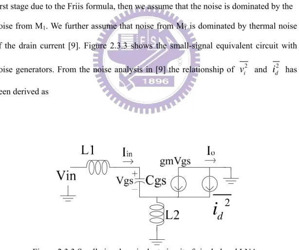
(20) Figure 2.3.2 Small signal equivalent circuit of the single-band LNA. 2.3.2 Noise Figure It is well-known that the noise figure of any cascade network is dominated by the first stage due to the Friis formula, then we assume that the noise is dominated by the noise from M1. We further assume that noise from M1 is dominated by thermal noise of the drain current [9]. Figure 2.3.3 shows the small-signal equivalent circuit with 2. noise generators. From the noise analysis in [9] the relationship of vi been derived as. id 2 Figure 2.3.3 Small-signal equivalent circuit of single-band LNA with noise generators. 8. 2. and id has.
(21) v = 2 i. id2 Gm. (2.9). 2. where Gm denotes the transconductance of the whole amplifier. Also Gm has been derived in terms of Vgs, Vin and gm as. Gm = g m. Vin 1 = gm V gs Z in jω C gs. (2.10). So the noise of the single-band LNA can be expressed as. ( Z ωC ) N + N in = 1 + r in gs NF = dev N in g m Rs. 2. (2.11). At matching condition, equation (2.11) becomes. NF = 1 + γ where Q=. Rs (ωcCgs ). 2. =1+. gm. γ g mQ 2 Rs. (2.12). 1 denotes the quality factor of the input series resonant circuit. R ω C s c gs. 2.3.3 Power Dissipation In this subsection, we derive the dependence of power dissipation on technology and circuit parameters under matching condition and for a given (Vgs-Vt) which is usually fixed for a design. First. P = I DVDD. (2.13). where ID is the drain current of M1. Since M1 operates in the saturation region, we have the equation. 1 W 2 I D = µCox (VGS − VT ) L 2. (2.14). Therefore we get. P ∝ µCox. W L 9. (2.15).
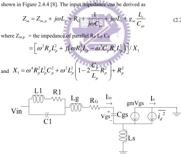
(22) 2 W W From Cgs = WLCox and g m = µ Cox (VGS − VT ) ∝ µ Cox , we have 3 L L. P ∝ µCox. W g m 2 L2 ∝ L Cgs µ. Furthermore, under matching condition Cgs = equation (2.6), and g m =. Rs Cgs L2. (2.16). 1. 1 , which is derived from ω ( L1 + L2 ) 2 c. , which is derived from equation (2.7), we have 2. L2 ⎛ Rs ⎞ 1 P∝ ⎜ ⎟ µ ⎝ ωc ⎠ 3 ⎛ L1 ⎞ L2 ⎜1 + ⎟ ⎝ L2 ⎠. (2.17). where L and µ are technology parameters, RS and ωc are constant in a certain design, and others are circuit parameters.. 2.4 Analysis of Concurrent Dual-Band LNA The concurrent dual-band LNA has been discussed and analyzed in recent years. [3,7] Of course the circuit analysis and noise model are also been established in some published papers. However these analyses are less helpful when designing the circuits because of the unreadable equations. In this section we try to derive some formulas using the methods used in the single band LNA. The input matching, noise figure and power dissipation are analyzed in terms of circuit elements under the two assumptions described in last section [10]. Some simulations are performed in this section to prove the analysis equations. Under these equations we kindly hope the designers could have strong impressions how to link the elements and the circuit performance, even inspire the motivation for some readers to study the more difficult theoretical circuit analysis about dual-band LNA derived in the above-mentioned papers.. 2.4.1 Input Matching Figure 2.4.1 shows the small-signal equivalent circuit of dual-band LNA. Applying KCL to the input loop in Figure 2.4.1 the input impedance can be derived as following. 10.
(23) Zin =. sL1 1 Ls + + + + + s L L R g ( ) g s G m sCgs Cgs 1−ω2LC 1 1. (2.18). where RG denote the gate distributed resistance of M1. The input impedance is designed to match 50Ω at both resonance frequency points of interest:. RG + g m. Ls = Rs Cgs. (2.19). sL1 1 + s ( Lg + Ls ) + =0 2 1 − ω L1C1 sC gs. (2.20). Solving equation (2.20), the two frequency points of interest can be obtained as 1/ 2. ⎛ X + X 2 +Y ⎞ ⎟ ω1 = ⎜ ⎜ 2 ( Lg + Ls ) L1C gs C1 ⎟ ⎝ ⎠. 1/ 2. ⎛ X − X 2 +Y ⎞ ⎟ ω2 = ⎜ ⎜ 2 ( Lg + Ls ) L1C gs C1 ⎟ ⎝ ⎠. where X denotes L1Cgs + Lg Cgs + Ls Cgs + L1C1 and Y denotes 4 ( Lg + Ls ) L1Cgs C1 .. Figure 2.4.1 Small-signal equivalent circuit of dual-band LNA. 2.4.2 Noise Figure Now we try to analysis a dual-band low noise amplifier in the similar way shown in subsection 2.3.2. The small-signal equivalent circuit of dual-band LNA with noise generator is shown in Figure 2.4.2. Figure 2.4.3 represents Figure 2.4.2 with 2. input-referred noise voltage vi. 2. and current ii at the input, followed by a noiseless 11.
(24) small-signal model of the amplifier with transconductance Gm. First of all it is easy to prove that equation (2.11) is also suitable for dual-band LNA. The equation tells us that (NF-1) is proportional to ( Z in ⋅ ω ) 2 . In order to find the. effect of finite Q inductor on noise, we take the series parasitic resistance of L1, which is represented as R1 , into consideration. Therefore the quality factor of L1, Q1can be expressed as. Q1 =. ωc L1. (2.21). R1. The not-quite-parallel RLC tank composed of R1, L1 and C1 can be converted to a purely parallel RLC tank composed of RP, LP and CP with the quality factor Q1 as shown in Figure 2.4.4 [8]. The input impedance can be derived as. Z in = Z in , p + jω Lg + RG +. 1 L + jω Ls + g m s jωC gs C gs. (2.22). where Zin,p = the impedance of parallel RP LP CP. = ⎡⎣ω 2 R p L2p + j (ω R p2 Lp − ω 3C p R p2 L2p ) ⎤⎦ / X 1 and. ⎛ ⎞ C X 1 = ω 4 R p2 L2pC p2 + ω 2 L2p ⎜1 − 2 p R p2 ⎟ + R p2 ⎜ ⎟ Lp ⎝ ⎠. id 2. Figure 2.4.2 Small-signal equivalent circuit of dual-band LNA with noise generators. 12.
(25) vi 2 ii 2. Zo. Zi. Figure 2.4.3 Representation of Figure 2.3.3 by two input noise generators. Figure 2.4.4 Purely parallel RLC tank. Figure 2.4.5 Input equivalent series RLC model. Also at matching condition, Zin matches to RS. 2 2 Ls ω R p L p Rs = Re ( Z in ) = RG + g m + Cgs X1. Leq = Lg + Ls +. L p R p2. 13. X1. (2.23). (2.24).
(26) 4 2 2 1 1 ω C p Rp Lp = + Ceq Cgs X1. (2.25). Hence we can redraw the input network in terms of RS, Leq and Ceq, as shown in Figure 2.4.5. The quality factor Qeq of the input network can be derived as. 1 Rs. Qeq = ≈. LeqCeq. 1 Rs Cgs. Lg + Ls +. L1. (2.26). L12 1 ω 2 2 − 2ω 2 L1C1 + 1 R1 Q1 2 c. From equation (2.10), we have the relationship of Vin and Vgs as. Vin 1 G = = m V gs Z in jω C gs g m. (2.27). For matching condition, we can rewrite equation (2.27) as. Vgs Vin. =. 1 Rs jωcC gs. =. Gm gm. (2.28). Now we try to express ωc in terms of Qeq and Ceq.. ωc =. 1 = LeqCeq. 1 Ceq. Leq Ceq. =. 1 1 1 = Ceq Qeq Req CeqQeq Rs. (2.29). Submitting equation (2.29) into equation (2.28), we have. Vgs Vin. =. QeqCeq jC gs. (2.30). which implies equation (2.31) 2. ⎛Q C ⎞ Gm2 = ⎜ eq eq ⎟ g m2 ⎜ C ⎟ ⎝ gs ⎠ Again submitting equation (2.31) into equation (2.9), we can get. 14. (2.31).
(27) vi 2 =. 4kTγ gm∆f 4kTγ g ∆f = 2 2 m 2 Gm gm Qeq (Ceq / Cgs )2. Finally the noise figure can be derived from (2.11) with N dev =. NF = 1 +. N dev N in. (2.32). vi2 as ∆f. vi2 Cgs2 γ γ ∆f =1+ =1+ ≈1+ 2 2 4kTRs g m RsQeq Ceq g m RsQeq2. (2.33). γ RsCgs. =1+ gm (Lg + Ls +. L1. ) L 1 ωc − 2ωc LC 1 1 +1 R Q12 2. 2 1 2 1. The noise figure of dual-band low-noise amplifier in equation (2.33) has a similar form to that of a single-band one in equation (2.12). The design concept that noise figure can be reduced by improving the quality factor of input matching series RLC tank, Qeq , under matching condition works in dual-band LNA design as well as in single-band one. Moreover we can improve Qeq by choosing inductor L1 with better Q1. To illustrate this in practice, we simulate the noise figure of the dual-band LNA with three inductors L1, which have Q-factor from 10 to 40. It can be seen in Figure 2.4.6 that the noise figure can be improved with better Q1.. 15.
(28) 8. Noise Figure (dB). 6. 4. Q=10 Q=20 Q=40. 2. 1G. 2G. 3G. 4G. 5G. 6G. 7G. Frequency (Hz). Figure 2.4.6 Simulation result of noise figure under different Q1. 2.4.3 Power Dissipation In this section, we will derive the dependence of power dissipation in the similar method used in 2.3.3. Under matching condition of dual-band LNA, equation (2.20) which implies that. C gs =. 1 ⎛. ωc2 ⎜ Lg + Ls + ⎝. ⎞ L1 ⎟ 1 − ωc2 L1C1 ⎠. (2.34). Also, from equation (2.19) we can get. gm =. Cgs Ls. ( Rs − RG ). (2.35). First substituting equation (2.35) into equation (2.16), we have 2. 2 ⎡ Cgs ⎤ 1 L2 Cgs 2 L P∝⎢ = 2 ( RS − RG ) ( RS − RG )⎥ µ ⎣ LS ⎦ Cgs µ LS. Finally substituting equation (2.32) into equation (2.36), we have. 16. (2.36).
(29) 2. L2 ⎛ Rs − RG ⎞ 1 P∝ ⎜ ⎟ µn ⎝ ωc ⎠ 3 ⎛ Lg ⎞ L1 LS ⎜1 + + ⎟ 2 ⎝ LS LS (1 − ωc L1C1 ) ⎠. (2.37). We get a similar result that the power dissipation is proportional to technology parameters, some standard constants and circuit parameters as equation (2.17). We can reduce the power dissipation by using larger LS from the equation (2.37). The dual-band LNA circuit is to be simulated with three different inductors LS. Figure 2.4.7 shows the relationship of the power dissipation of the dual-band LNA and the inductance of LS. In deed the power dissipation can be reduced by increasing LS. Moreover, the variance of LS will affect the input impedance so the choice of LS becomes the trade-off between power dissipation and input matching.. 8.8m 8.7m 8.6m. Power (W). 8.5m 8.4m 8.3m 8.2m 8.1m 8.0m 0.0. 500.0p. 1.0n. 1.5n. 2.0n. Inductance of Ls (nH). Figure 2.4.7 Simulation result of power dissipation under different LS. 17.
(30) 2.5 Layout Considerations The layout skill is very important for radio frequency circuit design because it may affect circuit performance very much. In this work we discuss three topics about the layout, the elements, the connections, and the element placement. To decrease noise the MOSFET is used as multi-finger, which is made of an array of 6 2.5µm/0.18µm MOSFETs. The 0.18µm (minimum) gate length was chosen to get the highest speed, and the 2.5µm gate width was chosen as a compromise between low polysilicon gate resistance and low drain/source contact resistance. The MIM (Metal-Insulator-Metal) capacitors without shield (the capacitance of per unit area ≈ 1 fF / µ m 2 ) and hexagonal spiral inductors (the Q-value is below 18) are used in this work. The poly without silicide resistance is used for gate bias. Guard-rings are added wit all elements to prevent substrate noise and interference. A shielded signal GSG pad structure is used in RF input and RF output to reduce the coupling noise from the noisy substrate. As for the connection lines, the power lines are considered for the current density while the signal lines are designed as short as possible. All interconnections between elements are taken as a 45∘corner. Last but not the least; the element placement also should be careful. Separate inductors away to decrease the mutual inductance. The RF input and the RF output are placed on opposite sides of the layout to avoid the high frequency signals coupling. The layout of the dual-band LNA is shown in Figure 2.5.1. The chip size is 1.32mm x 1.18mm. The chip photo is shown in Figure 2.5.2.. 18.
(31) Vdd. Vss Vin. Vout. Vb. Figure 2.5.1 Layout of the dual-band LNA. Figure 2.5.2 Chip Photo of the dual-band LNA 19.
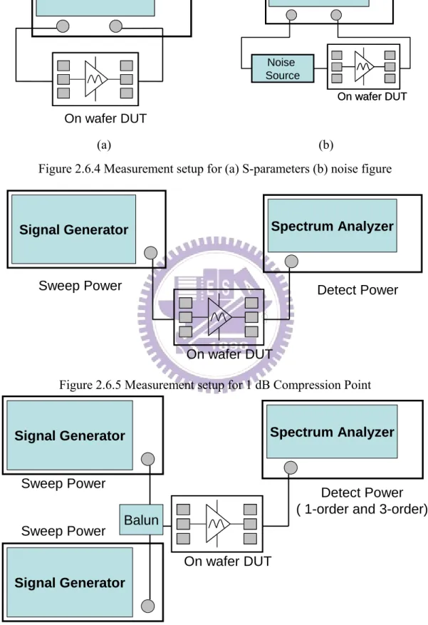
(32) 2.6 Measurement Considerations The dual-band LNA is designed for on-wafer measurement so the layout must follow the rules of CIC (Chip Implementation Center)’s probe station testing rules. This circuit needs two 3-pin DC PGP probes and two RF GSG probes for on-wafer measurement. The correlative rules are illustrated in Figure 2.5.1. Some other rules about layout are that the minimum distance of RF pad and DC pad are 200 um and the minimum pad size is 80um x 80um [11]. Figure 2.6.2 shows the on-wafer measurement setup with four probes. The top and bottom probes are DC PGP probes which provide the power supply voltage and bias voltage for the circuit. The left and right probes are RF GSG probes. A large coupling capacitor is needed in the input of the dual-band LNA to isolate the dc between circuit and equipment. Figure 2.6.3 is the picture of the on-wafer measurement setup with four probes. Figure 2.6.4 ~ Figure 2.6.6 show the measurement setup for S-parameters, noise figure, 1dB compression point and third-order intercept point. We use the RF IC measurement system powered by LabView to measure the linearity of the dual-band LNA. We will discuss the experimental and testing results of this circuit in following sections.. Figure 2.6.1 RF probe rules for measurement. 20.
(33) Vss. Vdd. Vin. Vout Vb. Vss. DC PGP Probe Figure 2.6.2 On-wafer measurement test diagram. Figure 2.6.3 Picture of on wafer measurement setup with four probes. 21. RF GSG Probe. RF GSG Probe. DC PGP Probe.
(34) Noise Figure Analyzer. Network Analyzer. Noise Source On wafer DUT. On wafer DUT (a). (b). Figure 2.6.4 Measurement setup for (a) S-parameters (b) noise figure. Spectrum Analyzer. Signal Generator. Sweep Power. Detect Power. On wafer DUT Figure 2.6.5 Measurement setup for 1 dB Compression Point. Spectrum Analyzer. Signal Generator. Sweep Power. Sweep Power. Detect Power ( 1-order and 3-order). Balun On wafer DUT. Signal Generator. Figure 2.6.6 Measurement setup for third-order intercept point. 22.
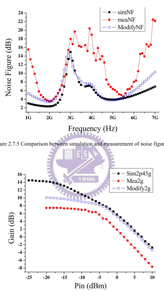
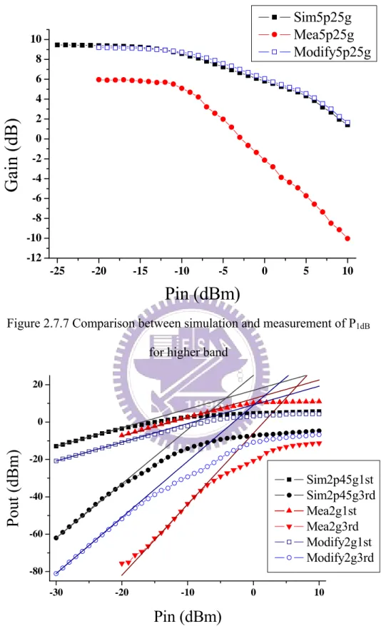
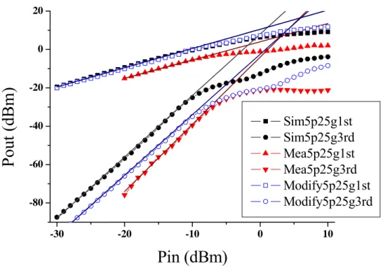
(35) 2.7 Experimental Results and Discussions The measured data reveals 7.45 dB and 6.06 dB power gain, -12.8 dB and -12.9 dB input return loss, 3.54 dB and 4.80 dB noise figure, -7.43 dBm and -9.66 dBm P1dB, and 6.84 dBm and 2.76 dBm IIP3 at 2GHz and 5.25Gz, respectively. From Figure 2.7.1 ~ Figure 2.7.4, It can be observed that the lower band of the dual-band LNA designed at 2.45GHz was shifted to 2GHz around while the higher band designed at 5.25GHz is roughly matched with simulation. The measured results reveal the fact that the most difficult part of the design is to provide exact input and output matching at both bands simultaneously with on-chip passive components. In other words the matching performance is very sensitive to variation of passive components, like inductors and capacitors. Fortunately the circuit has a fairly performance at the shifted band compared to the lower band, so the measured results at the shifted band is compared with the simulated performance at the lower band in stead of the measured results at the original band. Surely the reason why the lower band is shifted to 2GHz is also discussed in this section by modifying the original simulation results. The modified simulation gives us a reasonable explanation the difference between simulation and measurement. The measurement results reveal that the matching network of the dual-band LNA is not as well as what we expect, so we try to modify the simulation to fit the measurement results. We consider the ±10% variation of passive components while the size of the transistors is kept the same as original simulation. There are two reasons why we have to consider the variation of passive components though the physical models of the spiral inductors and MIM capacitors provided by the foundry were used in the simulation. First only some certain size of the spiral inductors are 23.
(36) measured and fitted. For example, the spiral inductor of W=15um, S=2um, R= 30um, 60um, 90um, 120um, and N=1.5, 3.5, 5.5 where W is the inductor track width, S is the spacing between tracks, R is the inner radius, and N is the number of turns. The inductance of the inductors whose size is not matched to the certain size is computed by interpolation or extrapolation using other measured physical models. For instance the spiral inductor L1 with size of W=15um, S=2um, R=72um, and N=3 might be computed form the inductor models with sizes of W=15um, S=2um, R=60um, 90um, and N=1.5, 3.5. The variation of the spiral model would be unignorable if the measured models are not very accurate, especially for the matching network sensitive to passive components. The similar problem also hit the models of MIM capacitors. The other reason is the parasitic capacitors from metal lines to substrate can not be predicted precisely though the layout parasitic extraction (LPE) had been applied on the design proceedings of the circuit design. According to the foregoing reasons we modified the dual-band LNA with variation of passive components to fit the measurement results. The comparisons of the simulation, measurement, and modified simulation results are shown in Figure 2.7.1 ~ Figure 2.7.9. These data are summarized in Table 2.7.1. The modified S-parameters are approximately fit to the measurement results in both frequency bands except for certain magnitude difference. This implies that the variation of passive components could course the shift of the frequency band. The measured linearity performances in both bands are better than modified simulation because of the degradation of the power gain. The measured noise figure is close to the modified simulation owing to the layout technique including the guard rings and shielding RF GSG pad. The measured results show the dual-band LNA achieves balanced performance at both the lower and higher band under low power consumption.. 24.
(37) 0. S11 (dB). -5 -10 -15 -20. sims11 meaS11 ModifyS11. -25 -30 0. 1G. 2G. 3G. 4G. 5G. 6G. 7G. Frequency (Hz) Figure 2.7.1 Comparison between simulation and measurement of S11. 20 10. S21 (dB). 0 -10 -20. sims21 meaS21 ModifyS21. -30 -40. 0. 1G. 2G. 3G. 4G. 5G. 6G. 7G. Frequency (Hz) Figure 2.7.2 Comparison between simulation and measurement of S21. 25.
(38) -20 -30 -40. S12 (dB). -50 -60 -70. sims12 meaS12 ModifyS12. -80 -90 -100 0. 1G. 2G. 3G. 4G. 5G. 6G. 7G. Frequency (Hz) Figure 2.7.3 Comparison between simulation and measurement of S12. 0. S22 (dB). -5 -10 -15 -20. sims22 meaS22 ModifyS22. -25 -30 0. 1G. 2G. 3G. 4G. 5G. 6G. 7G. Frequency (Hz) Figure 2.7.4 Comparison between simulation and measurement of S22. 26.
(39) simNF meaNF ModifyNF. 24 22. Noise Figure (dB). 20 18 16 14 12 10 8 6 4 2 1G. 2G. 3G. 4G. 5G. 6G. 7G. Frequency (Hz) Figure 2.7.5 Comparison between simulation and measurement of noise figure. Sim2p45g Mea2g Modify2g. 16 14 12 10. Gain (dB). 8 6 4 2 0 -2 -4 -6 -8 -25. -20. -15. -10. -5. 0. 5. 10. Pin (dBm) Figure 2.7.6 Comparison between simulation and measurement of P1dB for lower band. 27.
(40) Sim5p25g Mea5p25g Modify5p25g. 10 8 6. Gain (dB). 4 2 0 -2 -4 -6 -8 -10 -12 -25. -20. -15. -10. -5. 0. 5. 10. Pin (dBm) Figure 2.7.7 Comparison between simulation and measurement of P1dB for higher band 20. Pout (dBm). 0. -20. Sim2p45g1st Sim2p45g3rd Mea2g1st Mea2g3rd Modify2g1st Modify2g3rd. -40. -60. -80 -30. -20. -10. 0. 10. Pin (dBm) Figure 2.7.8 Comparison between simulation and measurement of IIP3 for lower band. 28.
(41) 20. Pout (dBm). 0. -20. Sim5p25g1st Sim5p25g3rd Mea5p25g1st Mea5p25g3rd Modify5p25g1st Modify5p25g3rd. -40. -60. -80 -30. -20. -10. 0. 10. Pin (dBm) Figure 2.7.9 Comparison between simulation and measurement of IIP3 for higher band. Table 2.7.1 Performance summary of concurrent dual-band LNA Specification. Simulation. Measurement. Modified Simulation. Frequency(GHz). 2.45. 5.25. 2. 5.25. 2. 5.25. S11 (dB). -18.4. -15.2. -12.8. -12.9. -18.4. -13.7. S21 (dB). 14.5. 9.47. 7.45. 6.06. 10.0. 9.30. S12 (dB). -37.6. -30.5. -28.0. -32.5. -46.07. -36.14. S22 (dB). -13.3. -13.9. -4.2. -3.8. -3.00. -7.43. NF (dB). 3.49. 3.97. 3.54. 4.80. 3.40. 4.00. Pin-1dB (dBm). -16.3. -10.4. -7.43. -9.66. -10.3. -7.18. IIP3 (dBm). -5.90. -1.32. 6.84. 2.76. -0.12. 6.09. Vdd (V). 1.8. 1.8. 1.8. Power (mw). 7.93. 7.21. 7.93. 29.
(42) 2.8 Comparisons Table 2.8.1 shows the comparisons of this work and recent dual-band LNA papers. It can be seen that the concurrent dual-band LNA presented in this chapter achieves a good performance with low power consumption. The circuit will be applied to a concurrent dual-band receiver front-end in the next chapter.. Table 2.8.1 Comparisons of concurrent dual-band LNA. Ref. [7]. Process. Frequency. S21. S11. NF. P1dB. IIP3. Band(Hz). (dB). (dB). (dB). (dBm). (dBm). 2.45G. 14 (Av). -25 *. 2.3. -8.5. 0. 5.25G. 15.5 (Av). -15 *. 4.5. -1.5. 5.6. Power. CMOS 0.35um. 10mw @2.5V. CMOS 0.18um. 14.2mw @ 1V. 2.4G. 11.6. -5.1. 2.3. -7.9. N/A. 5G. 10.8. -26.3. 2.9. -7.1. N/A. CMOS 0.25um. 19mw @1.5V. 1.8G. 18. -13. 3.5. N/A. N/A. 5.8G. 10. -10. 5. N/A. N/A. CMOS 0.25um. 31.2mw @ 2.5V. 2.45G. 13.2. -11.6. 1.7. -5.1. 10.1. 5.25G. 10.5. -8.3. 2.4. -5.1. 19.9. [3]. CMOS. 2.45G. 5.78. -20.4. 4.7. -3.5. 7. 2003. 0.25um. 37mw @ 2.5V. 5.25G. 3.24. -12.8. 5.69. 6.5. 17. This. CMOS. 7.21mw. 2G. 7.45. -12.8. 3.54. -7.43. 6.84. Work. 0.18um. @1.8V. 5.25G. 6.06. -12.9 4.80. -9.66. 2.76. 2002 [12] 2003 [13] 2003 [14] 2003 ※. ※:simulation results *:off-chip input matching network 30.
(43) Chapter 3 Concurrent Dual-Band Receiver Front-End. 3.1 Wireless LAN Standard Review In this section, we will review the wireless LNA standard, IEEE 802.11a, IEEE 802.11b and IEEE 802.11g. The IEEE 802.11b standard at the 2.4GHz ISM (industrial, scientific, and medical) band provides data rate up to 11Mbits/s with the direct sequence spread spectrum (DSSS). The standard was released by IEEE in 1999. The 802.11a standard at 5GHz U-NII band provides data rate up to 54Mbits/s using OFDM (orthogonal frequency division multiplexing) modulation. Released in 2003, the IEEE 802.11g standard, operating at the same band of 802.11b, uses OFDM modulation and provides data rate up to 54Mbits/s. In this section these three wireless LAN standards will be briefly described respectively.. 3.1.1 IEEE 802.11a As shown in Figure 3.1.1 the 802.11a standard has three U-NII (Unlicensed National. Information. Infrastructure). bands,. including. the. lower. band. (5.15GHz~5.25GHz), the middle band(5.25~5.35GHz) and the upper band (5.725GHz~5.825GHz). The lower and middle sub-bands accommodate eight channels in a total bandwidth of 200MHz. The upper band accommodates four. 31.
(44) channels in a bandwidth of 100MHz. The centers of the outermost channel shall be at a spacing of 30MHz from the edge of band for the lower and middle bands, and 20 MHz for the upper band. The bandwidth of each channel is 20MHz, and each channel has 52 sub-carriers for OFDM modulation with each sub-carrier has bandwidth of 312.5 KHz. Each sub-carrier can be either a BPSK, DQPSK, 16QAM, 64QAM signal. The data rate versus modulation is shown in Table 3.1.1. The input signal dynamic range is from -82dBm to -4dBm [15].. 30. 5150. 30. 20. 5250. 20. 5350. 20. 5725. 5825. 52 carriers, each BW= 312.5KHz. …. 20MHz. Figure 3.1.1 Channel allocation of IEEE 802.11a standard. Table 3.1.1 IEEE 802.11a modulation versus data rate. Modulation. Data Rate (Mbps). BPSK. 6,9. DQPSK. 12 , 18. 16QAM. 24 , 36. 64QAM. 48 , 64 32. MHz.
(45) 3.1.2 IEEE 802.11b IEEE 802.11b standard can be discussed by two operation areas: North American and European. The frequency range for North American is from 2400MHz to 2472MHz while the range for European is from 2400MHz to 2483.5MHz. Here we will discuss the North American operation. For non-overlapping operation three channels are used and the channel center frequencies are: 2412MHz, 2437MHz, and 2462MHz. As for overlapping operation, six channels are selected. The center frequency of each channel has a distance of 10MHz from others. Figure 3.1.2 shows the channel location of 802.11b standard. IEEE 802.11b provides a data rate up to 11Mbps and uses direct sequence spread spectrum (DSSS) and complementary code keying (CCK) modulation [16].. 2400. 2412. 2437. 2462. 2483.5 MHz. Non-overlapping. 2400. 2412. 10. 2462. 2483.5. MHz. Overlapping. Figure 3.1.2 Channel allocation of 802.11b standard. 3.1.3 IEEE 802.11g The operation frequency of 802.11g is from 2412MHz to 2483MHz, and the. 33.
(46) bandwidth of each channel is 20MHz. It extends the data rate of 802.11b to 54Mbps in the 2.4GHz band using OFDM modulation. Similar to 802.11b, 802.11g has three non-overlapping channels [17]. Table 3.1.2 lists the overview of IEEE 802.11a/b/g. Table 3.1.2 Overview of wireless LAN standard. Data Rate Modulation Mode (Mbps). Method. 6-54. Channel. Spectrum. Spacing. (MHz). (MHz). (MHz) 5150 - 5350. 802.11a. Available Frequency. 300. OFDM. 20 5725 – 5825. 802.11b. 1-11. CCK. 6-54. OFDM. 1-11. CCK. 802.11g. 2400 – 2483. 83.5. 25 25. 2400 - 2483. 83.5 25. 3.2 Review of Receiver Architecture The aggressive design goals of radio frequency transceivers may include low cost, low power dissipation, and small chip size. The architecture and frequency plan of the RF transceiver play an important role in the complexity and performance of the overall system. The base band signal feed into the transmitter is sufficiently strong, so there are fewer transmitter architectures thane those of receivers which small input signal is feed into. Some important issues such as noise, interference rejection, and band selectivity are serious discussed in the design of receivers. In this section we review some of recently popular receiver architectures, including heterodyne, homodyne, and low-IF. The benefits and drawbacks of them will be discussed in the following pages.. 34.
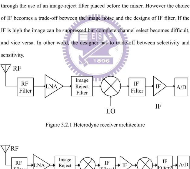
(47) 3.2.1 Heterodyne Architecture The first kind of receiver architecture is the heterodyne receivers shown in Figure 3.2.1. The RF input signal is firstly amplified, and then converted to a lower intermediate frequency (IF) by a local oscillator signal (LO). The low-noise amilifier (LNA) in front of the down-conversion mixer is used to amplify the RF signal and to reduce the noise figure of the following stage because of the high noise mixer. The IF filter suppress out-of-channel interferes and performs channel selection. This architecture suffers from a number of drawbacks. The problem of image is serious in heterodyne receivers. The most common approach to suppressing the image is through the use of an image-reject filter placed before the mixer. However the choice of IF becomes a trade-off between the image noise and the designs of IF filter. If the IF is high the image can be suppressed but complete channel select becomes difficult, and vice versa. In other word, the designer has to trade-off between selectivity and sensitivity.. RF RF Filter. Image Reject Filter. LNA. IF Filter. IF. A/D. IF. LO Figure 3.2.1 Heterodyne receiver architecture. RF RF Filter. LNA. Image Reject Filter. IF Filter1. LO1. IF1. IF Filter2. IF. LO2. Figure 3.2.2 Super-heterodyne receiver architecture 35. IF2. A/D.
(48) To solve the trade-off between selectivity and sensitivity, the super-heterodyne receiver, as shown in Figure 3.2.2, are presented. Most RF communication receivers use this conventional architecture. To release the requirement of filters’ Q- value we can down convert the RF signal by two steps, and perform the image rejection and channel selection between these stages. The drawback of super-heterodyne architecture is the numerous components. The filters which are commonly implemented with external SAW filters will be difficult to be integrated into a single chip while the on-chip filters would occupy unreasonable large areas.. 3.2.2 Homodyne Architecture Homodyne receivers, also called direct-conversion receivers or zero IF receivers, translates the RF signal directly to zero frequency. Figure 3.2.3 shows the architecture of the homodyne receivers. It has two important advantages over heterodyne architecture. First, the problem of image is circumvented because of zero IF. As a result, on image filter is required in front of the LNA. Second, the IF filters and subsequent down-conversion stages are replaced with low-pass filters and base-band amplifiers that are easy to monolithic integration. The drawbacks of the homodyne architecture may include the dc offset, I/Q mismatch, even-order distortion and flicker noise problem and the LO leakage to the antenna. The details about these problems and some possible solutions have been discussed in [18].. RF RF Filter. LPF. LNA. LO. VGA. IF. Figure 3.2.3 Homodyne receiver architecture 36. A/D.
(49) 3.2.3 Low-IF Architecture Comparing with the homodyne architecture converting the RF signal to zero IF directly, the other architecture converts the RF signal to low IF signal, which is so called low-IF architecture. Low-IF receiver architecture has gained much interest recently because it avoids the use of expensive discrete components such as image-reject filters, allowing a higher level of integration. As a non-zero IF receiver architecture, dc offset and LO self-mixing problems in low-IF receivers are not so severe compared to those in zero-IF receivers. On the other hand, low-IF receivers do have image problems. The most common techniques to remove the image in low-IF receivers are to use image reject architecture or polyphase filters [19]. The comparisons of these receiver architectures are summarized in Table 3.2.1. RF RF Filter. LNA. Filter. A/D. Low IF LO Figure 3.2.4 Low-IF receiver architecture. Table 3.2.1 Comparisons of different receiver architectures IF. Image reject. DC-offset. frequency. filter. problem. High. Off-chip. No. Low. Homodyne. Zero. None. High. High. Low-IF. Low. On-chip. No. High. Architecture. SoC. Heterodyne (Superheterodyne). 37.
(50) 3.3 Design of Concurrent Dual-Band Receiver Front-End In this section a new concurrent dual-band receiver using only one frequency synthesizer with tuning range of around 2.4 GHz for WLAN applications is introduced first. Figure 3.3.1 shows the concurrent dual-band receiver block diagram which has been proposed in [4]. It provides a RF concurrent dual-band receiver solution for IEEE 802.11a/b/g. The receiver consists of a differential concurrent dual-band LNA, a sub-harmonic mixer for 2.45GHz, a Gilbert-cell mixer modified from sub-harmonic topology for 5.25GHz, a quadrature voltage-controlled oscillator (VCO) and a multi-modulus frequency synthesizer. Appling such mixer operating at 2.45 GHz or 5.25 GHz with the same architecture can reduce the design complexity significantly. On-chip IF Gm-C filters are used for noise bandwidth limiting and anti-aliasing reasons. The concurrent dual-band receiver front-end is designed for this receiver block diagram as the marked area in Figure 3.3.1, which is designed and implemented cooperatively by the author and the other one [21]. Based on the comparisons of differential receiver architectures in last section, we choose low-IF receiver architecture in this work because of high degree of integration. The IF frequency is chosen at 10MHz because of the noise and receiver architecture considerations. The receiver frequency plan is shown in Figure 3.3.2. It can be seen that the tow LO frequencies are very close because of the usage of sub-harmonic mixer. Hence one frequency synthesizer is enough to provide the tuning range of LO signals around 2.4GHz. Compared with traditional topology with two Gilbert-cell mixers two frequency synthesizers may be needed owning to large frequency difference of two LO signals for two bands.. 38.
(51) This Work Dual-Band Antenna. 802.11a band. Sub-Harmonic Mixer Band-Pass Filter 10MHz. 4. Dual-Band LNA. 2. QVCO. To Baseband. 802.11b/g Gilbert Mixer band Figure 3.3.1 New concurrent dual-band receiver and concurrent dual-band front-end. DC. IF 10MHz. LO Image 2.44GHz RF 2.43GHz 2.45GHz. Frequency. (a) DC. IF 10MHz. LO 2.62GHz. (b). Image RF 5.23GHz 5.25GHz. Frequency. Figure 3.3.2 Receiver frequency plan (a) 2.45GHz (b) 5.25GHz. 39.
(52) The architecture of concurrent dual-band LNA for receiver front-end is shown in Figure 3.3.3. It has a similar architecture as the one discussed in last chapter except the spiral inductor Ls is replaced by the bondwire inductor Lbondwire1. Two other bondwires are needed in the RF input pad and power supply pad, so the input matching network and output matching network must be redesigned by considering the effect of the parasitic inductor from the bondwire. The inductance of bond wire is predicted as 1nH per 1mm length. Figure 3.3.4 illustrates the comparison of operation principles of conversional mixer and sub-harmonic mixer. The role of switching transistor (Qs) is evenly distributed to two parallel-connected transistors (Qs1, Qs2) in sub-harmonic mixer, thus it needs only half LO frequency compared to conversional mixer. Figure 3.3.5 and 3.3.6 show the topologies of the two mixers for receiver front-end. The design details about sub-harmonic mixer and Gilbert-cell mixer modified from sub-harmonic mixer can be found in [21]. The challenge of integrating LNA and mixers comes from the inter-stage design. In the design procedure we try to match the output matching of differential dual-band LNA and RF input matching of two mixers to the same impedance, for instance, 500 ohms parallel with 100pF, rather 50ohms. Large coupling capacitors are added between LNA and mixers for RF signal coupling and dc isolation. Some other circuits, like quadrature balun, balun, LO port matching network, and IF low-pass-filter, are implemented on PCB with lumped elements. The chip layout occupies area of 1.45mm x 1.45mm, and is shown in Figure 3.3.7. Figure 3.3.8 is the chip photograph of this work.. 40.
(53) Vdd=1.8V. Lbondwire3 On-chip C2. C3. Ld. L2. Vout Vbias Lbondwire2. Cout. M2 L1. Rb M1. Vin C1. Lg Lbondwire1. Figure 3.3.3 Concurrent dual-band LNA for receiver front-end. f IF. f RF. f LO LNA. Qs. RL. (a). f IF. 1/2 fLO,180. f RF Qs1. LNA Qs2. RL. 1/2 f LO,0. (b). Figure 3.3.4 Basic concept of (a) conversional mixer (b) sub-harmonic mixer 41.
(54) Vdd. RLn. RLp IF p IFn. LOp. M3. C4. LO. Balun. R3. M7. M4. M8. Vblo R4. M5. LOn. M9. C3 M6 C1. RFp. M10. M1. C2. M2. R1. RFn. R2. On-chip Vbrf. Vbrf. Figure 3.3.5 Gilbert-cell mixer for 2.45GHz front-end Vdd. RLn. RLp IFp IF n. LO. Quadrature Balun. LOp. C3 R3. Vblo. M7. R4. LOn. M4. C4 LOpj. M3. M8. C5 M5. R5. Vblo. M9. R6. LOnj. M6. C6. RFp. C1. M1. R1. M10 C2. M2. RFn. R2. Vbrf. Vbrf. On-chip. Figure 3.3.6 Sub-harmonic mixer for 5.25GHz front-end 42.
(55) Lop_5g. Lon_5g. LOpj_5g. RFp. LOnj_5g. IFp_5g RFn. IFn_5g IFp_2g IFn_2g. Lop_2g. Lon_2g. Figure 3.3.7 Chip layout of concurrent dual-band front-end. Figure 3.3.8 Chip photo of concurrent dual-band front-end. 43.
(56) 3.4 Experimental Results and Discussions The concurrent dual-band receiver front-end is measured by two PCB boards, 2.45GHz and 5.25GHz, rather one PCB board, because of large size off-chip passive baluns, too many on-board decoupling capacitors, and complicated dc bias routing for circuits. As shown in section 3.3, a balun for 2.44GHz and a quadrature balun for 2.62GHz are needed to provide differential and quadrature LO signals, which are shown in Figure 3.4.1 and 3.4.2, respectively.. Figure 3.4.1 Balun for 2.44GHz. Figure 3.4.2 Quadrature balun for 2.62GHz 44.
(57) The measured transmission coefficients of the 2.44GHz rat-race is. [ S ]rat −race. 0.689∠135.4° 0.016∠ − 94.2° ⎤ ⎡ 0.029∠117.4° 0.678∠135.56° ⎢0.678∠135.14° 0.045∠0.2° 0.024∠ − 161.7° 0.675∠ − 42.5° ⎥ ⎥ =⎢ ⎢0.688∠134.95° 0.023∠ − 162.5° 0.029∠34.6° 0.677∠137.62°⎥ ⎢ ⎥ 0.057∠41.1° ⎦ ⎣0.016∠ − 93.8° 0.675∠ − 42.1° 0.678∠138.15°. when all other ports are terminated with matched loads. The measured transmission coefficients of the quadrature balun composed of two rat-races and quadrature hybrid from port1 to port 2-port 5 are. S21 = 0.444∠ − 125.75° ; S31 = 0.442∠54.82° S41 = 0.452∠142.04°. ;. ; S51 = 0.452∠ − 35.27°. Selecting port 3 as phase reference we have phase relationship as Port 2:179.43∘. ;. Port 3:0∘. Port 4:87.22∘. ;. Port5:269.91∘. ;. The characteristic of quadrature balun satisfies the requirement for the LO port of sub-harmonic mixer though there are small phase and magnitude errors. PCB layouts and practical FR4 PCB circuits with SMA connectors are shown in Figure 3.4.3 and 3.4.4. There are some comments on PCB boards. Firstly the width of RF and LO signal paths on PCB are drawn as 50 ohms-line for impedance matching. Lumped Coupling capacitors (1uF) are placed in the RF paths for dc isolation. To filter out the ineluctable noise and spur from the power supplies we add four lumped decoupling capacitors (100pF, 10nF, 100nF, and 1uF) between each dc voltage and ground. IF low-pass-filters composed of lumped capacitors and resistors are placed at the IF outputs to depress the high frequency noise. The signal lines for differential or quadrature signals should be symmetric to avoid the phase error caused by the PCB transmission lines. The block diagram of PCB on board testing for dual-band receiver front-end is 45.
(58) shown in Figure 3.4.5. LO port has two paths for 2.45GHz front-end because of differential balun and four paths for 5.25GHz front-end because of quadrature balun. Two RF baluns are needed in the measurement, one for 2.45GHz and the other for 5.25GHz, to convert the RF signal from single to differential. The oscilloscope will be connected to the IF port to measure the output waveform because of 1M high input impedance.. IF OUT. IF OUT. RF IN. LOj IN. RF IN. LO IN. LOi IN. (a). Coupling Capacitors. (b). Decoupling Capacitors. IF LPF. Figure 3.4.3 PCB layout for (a)2.45GHz (b) 5.25GHz front-end. (b). (a). Figure 3.4.4 Photograph of PCB board for (a)2.45GHz (b)5.25GHz front-end. 46.
(59) DC Supplies. Balun. Signal Generator. RF. chip. Spectrum Analyzer. IF 50 Ω. LO 2/4. LO Matching Network 2/4. Signal Generator. (2.45GHz) / (5.25GHz). Balun / Quadrature Balun. Figure 3.4.5 Block diagram of PCB on-board testing for dual-band front-end. Table 3.4.1 summaries the performance of this work, including simulation and measurement results. The concurrent dual-band receiver front-end was fabricated using 0.18um CMOS 1P6M process. The RF input return loss of LNA are -15.9 dB and -15.8 dB at 2.45GHz and 5.25GHz, as shown in Figure 3.4.6. The LO port input return loss of two mixers are -13.4 dB and -13.1 dB, as shown in Figure 3.4.7 and 3.4.8. Figure 3.4.9 ~ Figure 3.4.12 show the measured linearity of the front-end characterized by the overall RF-to-IF -21.0 dBm and -15.3 dBm P1dB and the overall RF-to-IF -4.2 dBm and 4.9 dBm IIP3 for RF signals in two frequency bands. It demonstrates 17.2 dB and 11.8 dB voltage gain, 7.22 dB and 10.78 dB noise figure concurrently at two frequency bands with 28.8mw power dissipation. Finally the 10MHz output waveforms measured by oscilloscope are shown in Figure 3.4.13. Here are some discussions about the experimental results. The good RF input return loss may be owing to the accurate prediction of bondwire inductance and on-chip 47.
(60) circular spiral inductors which were designed, measured, and modeled by our group, rather foundry. The good LO input return loss comes from the accurate LO matching network composed of lumped inductors and capacitors. It may take great efforts to tune the matching network from the finite lumped element libraries. Although this work has good port input return loss, the performance of gain and noise figure does not meet our anticipation. There are three major factors. First, the inter-stage design may be interfered by the parasitic capacitors and resistors, causing the impedance mismatch between the output of differential dual-band LNA and RF input of mixers. Second, the quality factor Q values of the inductors are not good enough due to parasitic resistances. The Q-values of these inductors involved in this work is from 7.08 to 8.27. The gain and output matching of the concurrent dual-band LNA will be seriously affected by the poor Q-value of inductors. Finally the absence of output buffers at IF output impacts the driving capability of the front-end. These factors may depress the gain and increase noise figure of the concurrent dual-band receiver front-end.. Table 3.4.1 Performance summary of dual-band receiver front-end 2.45GHz Front-End. 5.25GHz Front-End. Sim.. Mea.. Sim.. Mea.. LO Power (dBm). -3. 8. -3. 7. RF Return Loss (dB). -18.4. -15.9. -13.4. -15.8. LO Return Loss (dB). -13.2. -13.4. -18.3. -13.1. Conversion Gain (dB). 14.7. 6.0. 2.57. -12.0. Voltage Gain (dB). 26.5. 17.2. 19.9. 11.8. Noise Figure (dB). 3.77. 7.22. 7.28. 10.78. P1dB (dBm). -20.6. -21.0. -22.1. -15.3. IIP3 (dBm). -7.8. -4.2. -4.5. 4.9. Power (mw). 17.9. 28.8. 17.9. 28.8. 48.
(61) Simulation Measurement. RF Port Return Loss (dB). 0. -5. -10. -15. -20. -25 0. 1G. 2G. 3G. 4G. 5G. 6G. 7G. Frequency (Hz) Figure 3.4.6 Comparison between simulation and measurement RF input return loss. Simulation Measurement. LO Port Return Loss (dB). 5. 0. -5. -10. -15. -20 2.0G. 2.2G. 2.4G. 2.6G. 2.8G. Frequency (Hz) Figure 3.4.7 Comparison between simulation and measurement LO input return loss of 2.45GHz Gilbert-cell mixer. 49. 3.0G.
(62) Simulation Measurement. LO Port Input Return Loss (dB). 5. 0. -5. -10. -15. -20 2.0G. 2.2G. 2.4G. 2.6G. 2.8G. 3.0G. Frequency (Hz) Figure 3.4.8 Comparison between simulation and measurement LO input return loss of 5.25GHz sub-harmonic mixer. Simulation Measurement. Conversion Power Gain (dB). 16 14 12 10 8 6 4 2 0 -2 -4 -40. -35. -30. -25. -20. -15. -10. Input RF Power (dBm) Figure 3.4.9 Comparison between simulation and measurement of P1dB of 2.45GHz front-end 50.
(63) Simulation Measurement. Conversion Power Gain (dB). 4 2 0 -2 -4 -6 -8 -10 -12 -14 -16 -40. -35. -30. -25. -20. -15. -10. Input RF Power (dBm) Figure 3.4.10 Comparison between simulation and measurement of P1dB of 5.25GHz front-end 20. IF Output Power (dBm). 10 0 -10 -20 -30. Sim_Fundamental Sim_IM3 Mea_Fundamental Mea_IM3. -40 -50 -60 -70 -30. -25. -20. -15. -10. -5. 0. RF Input Power (dBm) Figure 3.4.11 Comparison between simulation and measurement of IIP3 for 2.45GHz front-end. 51.
(64) 0. IF Output Power (dBm). -10 -20 -30 -40 -50. Sim_Fundamental Sim_IM3 Mea_Fundamental Mea_IM3. -60 -70 -30. -25. -20. -15. -10. -5. 0. 5. RF Input Power (dBm) Figure 3.4.12 Comparison between simulation and measurement of IIP3 for 5.25GHz front-end. VIFp = 125.0mV. VIFp = 112.5mV. VIFn = 123.4mV. VIFn = 121.9mV. Frequency =10.01MHz. Frequency =10.00MHz. (a). (b). Figure 3.4.13 Output waveform of (a) 2.45GHz (b) 5.25GHz front-end. 52.
(65) 3.5 Comparisons Table 3.5.1 shows the comparisons of this work and other recently dual-band receiver front-end papers. Compared with other dual-band front-end this work achieves comparable performances with nearly equal chip area and lower power dissipation under concurrent operation for two frequency bands. Table 3.5.1 Comparisons of dual-band receiver front-end Ref. [2] 2004. [22] 2004. [23] 2005. This Work. CMOS. CMOS. CMOS. CMOS. 0.18um. 0.18um. 0.18um. 0.18um. 41.5mw. 24mw. 53.9mw*. 17.9mw. 28.8mw. @1.8V. @1.8V. @1.8V. @1.8V. @1.8V. Process. Power Frequency (GHz). 2.4. 5.15. 2.4. 5.2. 2. 5. 2.45. 5.25. 2.45. 5.25. Gain (dB). 39.8. 29.2. 20. 18.8. 33. 31. 26.5. 19.9. 17.2. 11.8. S11 (dB). -8. -10.8. N/A. N/A. <-15. NF (dB). 1.5. 4.1. 3.1. 3.55. 4.7. 5.1. 3.77. P1dB (dBm). -21. -12. N/A. N/A. N/A. N/A. -20.6 -22.1 -20.0 -15.3. IIP3 (dBm). -12.7. -4.1. -13.4 -11.4. -1. -11.8. -7.8. <-15 -18.4 -13.4 -15.9 -15.8 7.28. -4.5. -4.2. 10.7. 4.9. Condition. Mea.. Mea.. Mea.. Architecture. switched dual-band LNA+ Gilbert mixers. concurrent dual-band LNA + Gilbert mixers. two LNAs + Gilbert mixers. sub-harmonic mixers. 0.98 x 1.13. 1.21 x 1.46. 1.4 x 3.5. 1.45 x 1.45. Chip area (mm2). *:IF mixer is included 53. Sim.. 7.22. Mea.. concurrent dual-band LNA +.
(66) Chapter 4 Low-Voltage Micromixer. 4.1 Review of Basic Micromixer The down-conversion mixer is a key building block in a receiver system. Its main function is to translate the incoming RF signal to an intermediate frequency for further processing. It dominates the system linearity and determines the performance requirements of its adjacent blocks. Among many proposed active mixers the Gilbert-cell mixer has been widely used because of it’s LO suppression at the IF output. However the circuit linearity is limited by MOSFET transistor linearity, which is the common source MOSFET transconductance [24]. The small-signal linearity of the input stage, and thus the third-order intercept point, can be greatly improved using several techniques, notably, source degeneration, the multi-tanh doublet and triplet. However the 1-dB gain compression point still falls short of what may be required in handling large input signals without significant intermodulation. Further these RF stages do not provide an accurate match to the source [25]. Therefore the micromixer was proposed in [25] to overcome these problems. The topology of the basic micromixer is shown in Figure 4.1.1. The micromixer follows the general form of Gilbert-cell mixer except for the use of a bisymmetric class-AB RF stage based on the translinear principles while the mixer core is identical to the Gilbert-cell mixer. The class-AB RF stage provides well-defined matching impedance and much lower input related nonlinearity.. 54.
(67) Figure 4.1.1 Basic micromixer. Although the micromixer does not have inherent gain compression in RF stage, the 1-dB compression point of the micromixer will often be determined by limitations on the output IF signal amplitude, rather than by the RF stage. The noise figure of the micromixer depends on design details and is acceptable for many receiver applications although it is generally not as low as in mixers specially optimized for noise performance. In Figure 4.1.1, Q1 can be viewed as a grounded-base stage. It delivers its output I1 to the mixer pair QM1-QM2 in phase. It can, in principle, handle unlimited amounts of current during large negative excursion of VGEN. On the other hand, the current mirror sub-cell Q2-Q3 can handle essentially unlimited amounts of current during positive excursion of VGEN both at its input node and at its inverted-phase current output I3, which drives QM3-QM4. Acting together, these two sub-cells provide an 55.
(68) overall transfer characteristic which is symmetric to both positive and negative inputs, and which is in principle not limited by the choice of bias level. The differential current output I1-I3 is linear with IRF, although the individual currents are quite nonlinear. [25] Because of the advantage of easily matching and wide dynamic range the micromixer is also applied to the CMOS process in recently years [26]. Replacing the BJT with MOSFET, we can derive two simple expressions for low-frequency small-signal input resistance and voltage gain under the assumption of ideal transistors and neglecting parasitic effects for simplifying [27]. The low frequency small-signal input resistance of RF input stage is approximately R IN = Re(Z in ) =. 1 2g m. (4.1). which implies the micromixer RF input stage can be matched to 50Ω as long as we choose proper bias current. Assume perfect impedance matching to 50Ω, the low frequency small-signal voltage gain is approximately GV ≡. V IF 1 2 2 ≈ ⋅ g m ⋅ ⋅ 2 RL = ⋅ g m RL V RF 2 π π. (4.2). These two equations will be very helpful when designing the micromixer.. 4.2 Low-Voltage Micromixer In recent years low-voltage circuit design has become an important issue because of the consideration of battery design and power reduction. However the traditional micromixer is inapplicable for the low voltage design due to the stack of the four stage cascode architecture. Here we propose a modified micromixer applicable for low-voltage operation, as shown in Figure 4.2.1.. 56.
(69) The main improvement of the low-voltage micromixer is the RF stage, while the switch-stage of the low-voltage micromixer is identical to the basic micromixer. The RF signal is feed in between R1 and M2, and coupled to the RF stage by CcRF1 and CcRF2. We bias the transistors M1 and M2 separately using Vg1 and Vg2. The improved RF stage overcomes the bias-relative problem and retains the characteristic of class. Figure 4.2.1 Low-voltage micromixer LLOn. CcLOn LOn. LOng Rbn. CLOn1. CLOn2. VbLO. LOp. LLOp. CcLOp. LOpg Rbp. CLOp1. CLOp2. VbLO. Figure 4.2.2 LO matching network 57.
數據
+7
相關文件
由圖可以知道,在低電阻時 OP 的 voltage noise 比電阻的 thermal noise 大,而且很接近電阻的 current noise,所以在電阻小於 1K 歐姆時不適合量測,在當電阻在 10K
一般我們如過是透過分享器或集線器來連接電腦 的話,只需要壓制平行線即可(平行線:兩端接 頭皆為EIA/TIA 568B),
一般我們如過是透過分享器或集線器來連接電腦 的話,只需要壓制平行線即可(平行線:兩端接 頭皆為 EIA/TIA 568B ), 如果是接機器對機器 的話,需要製作跳線( Crossover :一端為
油壓開關之動作原理是(A)油壓 油壓與低壓之和 油壓與低 壓之差 高壓與低壓之差 低於設定值時,
請繪出交流三相感應電動機AC 220V 15HP,額定電流為40安,正逆轉兼Y-△啟動控制電路之主
首先,在前言對於為什麼要進行此項研究,動機為何?製程的選擇是基於
Abstract - A 0.18 μm CMOS low noise amplifier using RC- feedback topology is proposed with optimized matching, gain, noise, linearity and area for UWB applications.. Good
傳統的 RF front-end 常定義在高頻無線通訊的接收端電路,例如類比 式 AM/FM 通訊、微波通訊等。射頻(Radio frequency,
