國 立 交 通 大 學
電子物理研究所碩士班
碩 士 論 文
鎳金屬誘發側向結晶垂直通道
低溫複晶矽薄膜電晶體之研究
The Study of Vertical Channel LTPS TFTs with
Metal-Induced Lateral Crystallization Method
研 究 生:郭 柔 含
指導教授:趙 天 生 博士
鎳金屬誘發側向結晶垂直通道
低溫複晶矽薄膜電晶體之研究
The Study of Vertical Channel LTPS TFTs with
Metal-Induced Lateral Crystallization Method
研 究 生:郭柔含 Student:Rou-Han Kuo
指導教授:趙天生 博士 Advisor:Dr. Tien-Sheng Chao
國 立 交 通 大 學
電子物理研究所碩士班
碩 士 論 文
A Thesis
Submitted to Department of Electrophysics
College of Science
National Chiao Tung University
in Partial Fulfillment of the Requirements
for the Degree of Master of Science in Electrophysics
June 2012,
Hsinchu, Taiwan, Republic of China
中華民國 一百零一 年 六 月
I
鎳金屬誘發側向結晶垂直通道低溫複晶矽薄膜電晶體之研究
研 究 生:郭 柔 含 指導教授:趙 天 生 博士
國 立 交 通 大 學
電 子 物 理 系 碩 士 班
摘要
多晶矽薄膜電晶體擁有較高的載子遷移率,被認為可廣泛應用於主動矩陣式 液晶顯示器的主動開關元件上。為了提升元件特性,元件的通道長度的微縮是有 必要的。然而,垂直通道結構的複晶矽薄膜電晶體的通道長度是以沉積的閘極厚 度所決定,並不受微影機台的限制,因此具有高度的發展潛力可應用於三維垂直 整合。但過多的晶粒界面及缺陷存在於通道中將大幅地劣化多晶矽薄膜電晶體的 特性。 在本論文中,我們利用了金屬誘發側向結晶的方式製作垂直通道的多晶矽薄 膜電晶體,其製程簡單,並不需要額外的光罩並與 CMOS 製程有高度相容性,且 其具有等效的雙閘極結構,能有效地抑制汲極端的電場以降低漏電流並提升開關 電流比。 本研究提出利用氨電漿處理及結晶過濾效應可有效地提升元件特性。研究中 發現,較窄的結晶通道寬度具有較佳的結晶特性及較少的晶界缺陷,因此我們可 利用較窄的結晶過濾寬度來有效地提升元件特性。此外,我們也比較了以鎳金屬 誘發側向結晶及鎳金屬矽化物誘發側向結晶的差別。由結果顯示,兩種方式並沒 有太大的差異。推論由鎳金屬矽化物誘發側向結晶的方式無法有效地進一步降低 在通道中的鎳金屬含量。但藉由結晶過濾效應,兩種結晶方式都可利用通道個數 的增加來提升元件的開關電路比,且並不影響其他電性表現。II
The Study of Vertical Channel LTPS TFTs with Metal-Induced
Lateral Crystallization Method
Student:Rou-Han Kuo Advisor:Dr. Tien-Sheng Chao
Department of Electrophysics
National Chiao Tung University
Abstract
Polycrystalline silicon thin-film transistors (poly-Si TFTs) have attracted considerable attention because of its application in active matrix liquid crystal displays (AMLCDs), due to their higher mobility than amorphous silicon (a-Si) TFTs. There is a need to scale down poly-Si TFTs’ channel length to achieve higher speeds and packing densities. Therefore, vertical-channel thin-film transistors (VTFTs) have been widely researched and developed to overcome the limits of photolithography. VTFTs have shown great potential for 3-D integration since the channel lengths are determined by the thicknesses of the poly-Si or SiO2 film, instead of photolithographic process
limitations.
In this thesis, we have fabricated the VTFTs with MILC technology. They are simple in structure and fabrication of VTFTs without any additional mask and compatible with the silicon technology. Moreover, VTFT structure which has the inherently own an effective dual-gate structure. And it can reduce the peak lateral electrical field in the drain depletion region, significantly reducing the leakage current and increasing the Ion /Ioff current ratio.
We have proposed that the NH3 plasma treatment and crystal filtering effect can
improve the electrical performance of VTFTs. In our research indicates that the narrower channel width has the better the electrical performance and less intra-grain defects and grain boundary. Thus, the high performance VTFTs can be achieved by
III
reducing the channel width. Compare MILC-VTFTs with NSILC-VTFTs, we can observe that the electrical performance of them seems to be no significantly difference. The method of NSILC is not able to reduce the Ni and NiSi2 efficient and further
improve the device characteristics. Both the MILC-VTFTs and NSILC-VTFTs can be improved the crystal filtering effect and multiple channel structure.
IV 誌謝 兩年,說長不長說短不短的時間,我學習到了很多道理,也有所長進了吧?! 首先,最應該要感謝的,就是實驗室的大家長:趙天生老師。謝謝老師當初肯辜 負眾學長的期待選擇看似上進乖巧的我作為實驗室的新力軍。老師以淡定哲學領 導著一個向心力如此強大的團隊,讓我們可以盡情地做自己想做的事!我想,這些 年的研究成果都足以說明無為而治的潛在力量。這一路以來也受到很多人的幫助, 我才得以順利完成學位。最應該感謝的人就是吳翊鴻學長(小胖)及呂宜憲學長(阿 壘)。我想應該沒有第二個學弟妹可以同時收集到『NDL 雙煞』的暴怒紅牌吧! 正 所謂愛之深責之切,從你們身上獲得了太多太多的關愛及幫助,這學位可說是你 們賜予的。此外,也要謝謝郭柏儀學長在實驗及生活經驗上熱情分享,總讓我充 滿動力;呂侑倫學長(Allen)總不忘在落井下石後偷偷地拉我一把;江宗育學長默 默的提點我做人處事及學習上應有的態度;林哲緯學長成熟穩重的男人哲學;王 冠迪學長的禪定態度;廖家駿學長在學問及處事上的分享;嚴立丞學長(阿堂)擔 任夜間部班長期間的輔導及接送;陳昱旋學姊(肉肉)照護我的生活起居,一手包 辦生活上的瑣碎雜事;張添舜學長的游擊狙擊手人生;李時璟學長以德報怨地接 納我的無禮;林玉喬學姐帶給實驗室許多生活樂趣;卓大鈞學長親切的為人及口 吻讓我覺得有股安定感;林哲毅學長稱職的夜間警衛默默守護實驗室;小阿昌和 小劉的深夜連環炮;其儒的溫文有禮;立盈遠方的祝福;同窗劉劭軒(小劉)詼諧 風趣的言談使我思想更為多元;好朋友唐明慈讓我的碩班生活增添許多精彩;NFC 二哥解偉斌的義氣相挺;EF554 妹婿貽泓、文武雙全的儀儒、樂觀開朗的樂樂及 無聲無息的小小等。短短的研究所生涯,發生了很多事,謝謝各位學長姐不斷地 幫我收拾善後。因為有你們,小紅的碩士班人生得以平安順利。 此外,更要謝謝一群從大學陪伴我至今的好友們:曼麗、詩涵、堯薇、好長、 小柏、宇晟、蔡、西瓜及一同長大的琇怡。一路上發生的大小事都能有你們的參 與、扶持,真的很令人安心。因為有你們,生活多了些歡樂,少了點憂慮。
V
最後,由衷地感謝我的家人。謝謝爸媽總不辭辛勞地教導養育我長大,所有 的成就都是你們賜與我的;謝謝哥哥及弟弟在生活上的扶持,你們是我最堅強的 後盾。希望這小小的成就可以帶給你們小小的驕傲!
VI
Contents
Abstract (Chinese)... I.
Abstract (English)... II.
Acknowledge... IV.
Contents... VI.
Table Captions... VIII.
Figure Captions... IX.
Chapter 1 Introduction... 1
1.1
Overview of Poly-Si Thin-Film-Transistors (TFTs)...
1
1.1.1
Solid-Phase Crystallization (SPC)...
3
1.1.2 Excimer Laser Crystallization (ELC) ... 4
1.1.3 Metal-Induced Lateral Crystallization (MILC) ... 4
1.2
Overview of Vertical Channel Thin-Film-Transistors
(VTFTs) ...
6
1.3
Motivation...
7
1.4
Thesis Organization... 9
Chapter 2 Experimental process and Electrical parameters
extraction...
12
2.1
Fabrication
of
the
vertical
channel
thin-film
transistor...
12
2.1.1 Fabrication process... 12
2.1.2 Fabrication results... 13
2.2
Method of Device Parameter Extraction... 14
2.2.1 Determination of Subthreshold Swing... 14
VII
2.2.3
Determination of On/Off Current Ratio...
16
Chapter 3 Characteristics of Vertical Channel Low
Temperature Nickel Induced Lateral Crystallization Poly-Si
TFT………
26
3.1
Effect of post-treatment... 27
3.2
Crystal Filtering effect... 28
3.3
Compare NSILC-VTFT with MILC-VTFT... 31
Chapter 4 Conclusions and Future Works... 50
4.1
Conclusion... 50
4.2
Future works …... 51
VIII
Table Captions
Table 3-1 Characteristics of poly-Si TFTs with and without plasma
treatment. All parameters are extracted at Vd = 0.1 V. W/L = 0.35 μm/ 1 μm………...…...… 35
Table 3-2 The width and number of unit channel in the devices.…….…... 36
Table 3-3 The statistical average value of some parameters of EW2 and
EW1. ……….……... 43
Table 3-4 Comparison the statistical average value of NSILC-VTFTs and
IX
Figure Captions
Chapter 1
Fig. 1-1 Schematic of field-effect transistor. ……….…... 10
Fig. 1-2 The crystalline structure of Si and NiSi2. ……….. 10 Fig. 1-3 Schematic equilibrium molar free-energy diagram for NiSi2 in
contact with a-Si and c-Si. ………..…...….. 11
Fig. 1-4 Schematic of the growth mechanism of Ni-induced lateral
crystallization………..……….. 11
Chapter 2
Fig. 2-1 The schematic cross-section diagrams and key process flows of
the devices. ………..……...…….. 17
Fig. 2-2 Device structure of the proposed VTFT. ………..………. 20
Fig. 2-3 The cross-sectional transmission electron microscope (TEM)
microphotograph and TED pattern of the NSILC-VTFTs. …..….. 21
Fig. 2-4 The cross-sectional transmission electron microscope (TEM)
microphotograph and TED pattern of the MILC-VTFTs………… 22
Fig. 2-5 The top-view schematic diagram of MILC-VTFTs with source,
drain, bottom gate and Ni-window. ………...……… 23
Fig. 2-6 (a) The cross-sectional schematic diagram of MILC-VTFTs and
(b) Effective dual gate structure of MILC-VTFTs. ……... 23 Fig. 2-7 Optical microscopy photograph of active pattern with the source,
X
the drain, channels, bottom-gate and Ni-seeding window. ……….. 24
Fig. 2-8 The OM micrographs of a sample heat treated for (a) 3 h and (b)
12 h of heat treatment at 500 oC, and the whole active channel was crystallized by the MILC process. ……….. 25
Chapter 3
Fig. 3-1 The typical transfer characteristic and the transconductance of
(a) NSILC-VTFTs and (b) MILC-VTFTs with and without NH3 plasma treatment. ………...… 34
Fig. 3-2 The top view optical microscope microphotograph of
MILC-VTFTs with various widths of crystal filter. (a) Total width
= 2 μm (b) Total width = 1μm ………... 37
Fig. 3-3 The transfer characteristics of MILC-VTFTs with various widths
of crystal filter. (a) Effective widths = 2 μm (b) Effective widths =
1 μm………... 38
Fig. 3-4 The statistical average values of on-state current of group
EW2……….…... 39
Fig. 3-5 The statistical average values of off-state current of group
EW2………..……. 39
Fig. 3-6 The statistical average values of subthreshold swing of group
EW2. ……….………..….. 40
Fig. 3-7 The statistical average values of transconductance of group
EW2...………..…….. 40
XI
EW1…...………..….. 41
Fig. 3-9 The statistical average values of off-state current of group
EW1…….………..……… 41
Fig. 3-10 The statistical average values of subthreshold swing of group
EW1. ………... 42
Fig. 3-11 The statistical average values of transconductance of group
EW1. ……….... 42
Fig. 3-12 Comparison the on-state current distribution of NSILC-VTFTs
and MILC-VTFTs with various channel width………... 44
Fig. 3-13 Comparison the off-state current distribution of NSILC-VTFTs
and MILC-VTFTs with various channel width. ………...… 44
Fig. 3-14 Comparison the subthreshold swing distribution of
NSILC-VTFTs and MILC-VTFTs with various channel width... 45
Fig. 3-15 Comparison the transconductance distribution of NSILC-VTFTs
and MILC-VTFTs with various channel width………. 45
Fig. 3-16 The transfer characteristics of a MILC-VTFT with unit crystal
width of 0.35 μm under various channel number. ………... 47
Fig. 3-17 The on-state current distribution of NSILC-VTFTs and
MILC-VTFT with unit crystal width of 0.35 μm under various
channel number. ………..… 48
Fig. 3-18 The off-state current distribution of NSILC-VTFTs and
MILC-VTFT with unit crystal width of 0.35 μm under various
channel number. ………... 48
Fig. 3-19 The subthreshold swing distribution of NSILC-VTFTs and
XII
channel number. ………..…… 49
Fig. 3-20 The transconductance distribution of NSILC-VTFTs and
MILC-VTFT with unit crystal width of 0.35 μm under various
channel number. ………....….. 49
Chapter 4
Fig. 4-1
The schematic cross-section of VTFT with O/N/O layer
and double-gate.
………..……….. 521
Chapter 1
Introduction
Low-temperature polycrystalline silicon (LTPS) thin-film-transistors (TFTs) have attracted considerable interest due to their wide applications in active matrix liquid crystal displays (AMLCDs) [1]-[3], driving circuit of system-on-panel (SOP) [4]-[5], nonvolatile memory, image sensors, photo-detector amplifier, and 3-D circuit integration [6], because they provide good electrical properties and can be integrated in peripheral circuits on inexpensive glass substrates. Among these applications, the application in the AMLCD was the major driving force to promote the developments of poly-Si TFTs technology. Therefore, how to improve the performance of LTPS TFTs is an interesting and important issue.
1.1 Overview of Poly-Si Thin-Film-Transistors
Thin film transistor (TFT) is one of the field-effect transistors, which is composed of three terminals including a gate, a source and a drain as shown in Fig. 1-1. The transistor may conduct current between the source and drain if a channel of carrier is created by making the gate voltage (VG) sufficiently large. Thus, the magnitude of the
current can be controlled by the gate voltage. Take n-type transistor for example. When the VG becomes sufficiently positive, free electrons are attracted to the oxide/ Si
interface, forming the conductive channel. We say the transistor is on. The gate potential at which the channel begins to appear is called the “threshold voltage” Vt. If
the VG < Vt, no channel exist, the device is off.
The TFT employ a thin semiconductor film on an insulating substrate as the active device channel. And the TFT was first demonstrated in 1961 by Dr. P. K. Wedsnimer.
2
With its simplicity in structure and fabrication, the applications of TFTs are becoming more and more popular.
In the beginning, the a-Si:H (hydrogenated amorphous silicon) TFTs were applied as the pixel switching device in the AMLCDs. The major advantage of a-Si TFTs is appropriate for large area glass substrate with the lower processing temperature (T < 350 oC). However, the application of a-Si TFTs is constrained in the aspect of pixel
switching elements. Hence, it is difficult to integrate pixel switching elements and peripheral driving circuits on the same glass substrate for system-on-panel due to the low carrier field-effect mobility (below 1 cm2/V-s generally) of the a-Si:H TFTs. In
order to acquire devices suitable for system-on-panel, it is necessary to fabricate the devices with low cost, high electrical properties and reliability by low temperature process.
Since the first poly-Si TFTs were fabricated by Fa et al in 1966 [7], the electrical properties, conduction mechanism and fabrication process of poly-Si films were extensively studied [8]-[9]. Over the past three decades, poly-Si TFTs have been drawn much attention thanks to the fact that they can be fabricated with a low thermal budget and on large area substrates while achieving performances adequate for the realization of complex circuit. For this reason, they have many commercial applications.
Recently, poly-Si has been proposed as a very attractive alternative material for the AMLCDs because of their superior performance [10]-[12]. The mobility of poly-Si can reach 10 to 300 cm2 /V-s, so the devices with considerable high driving current can
be integrated of peripheral circuit on the same panel in AMLCDs [13]. However, the conduction mechanism and performance of poly-Si TFTs are strongly influenced by grain boundaries and intra-grain defects. The defects in the grain boundary would trap carriers and build a potential barrier which degrades the on-state current and subthreshold swing (S.S.). Moreover, the grain boundary also provides the path of
3 leakage current.
In order to enhance the performance of the poly-Si TFTs, several methods have been proposed to improve the device performance such as enlarging the grain size of poly-Si films and reducing the trap-state densities in the grain boundaries. It has been reported that the a-Si films can be crystallized by many techniques, such as Solid-Phase Crystallization (SPC) [13]-[15], Excimer Laser Crystallization (ELC) [16]-[17] and Metal-Induced Lateral Crystallization (MILC) [18]-[20] to obtain the large grain size of poly-Si to raise the field-effect mobility. Besides, there were other methods such as plasma treatment to passivate the defects in the channel or narrowing the channel width to reduce the trap state density. These techniques are described as follow.
1.1.1 Solid-Phase Crystallization (SPC)
The a-Si film was deposited at temperature below 600 oC, so the film was required
thermal energy to convert amorphous silicon into the polycrystalline form. This method is called Solid-Phase Crystallization (SPC). The SPC technique is usually performed at 600 oC for 24~72 hours. The SPC method has many advantages, such as simplicity,
low-cost batch process, and compatible with the silicon technology, large area capability, and smoother surface. However, such crystallized poly-Si films have high density of grain-boundary defects and intra-grain defects, which degrade the electrical properties of poly-Si TFTs. But the high crystallization temperature around 600 oC
prevents SPC from commercial application. Because the maximum process temperature of the inexpensive glass substrate is limited to less than 600 oC. If
temperature up to 600 oC, the substrate might be bending, it would affect the following
process of fabrication.
4
Excimer Laser Crystallization (ELC) has investigated as an alternative crystallization technique to furnace annealing. And the standard gas mixtures and output wavelengths are ArF (193 nm), KrF (248 nm) and XeCl (308 nm). For fabricating high performance poly-Si TFTs on a glass substrate, Excimer Laser Crystallization method is very promising for the following reasons. First of all, the combination of strong optical absorption of the UV light in silicon (α>106 cm-1) and
small heat diffusion length (~100 nm) during the laser pulse (10 ns~30 ns) implies that high temperature can be produced in the silicon surface region. Therefore, we can obtain higher quality poly-Si film without damage of the glass substrate by serious thermal shrinkage. Second, it can crystallize the film selectively by partially irradiating the film surface, so both poly-Si TFTs and a-Si TFTs can be formed on the same substrate. Third, the throughput of the ELC process is higher than that of the SPC process and the large grain size translates to fewer defects.
However, there are many problems need to be resolved to obtain a mature ELC poly-Si TFT technology, such as high manufacturing cost, high process complexity, narrow laser process window, the roughness and uniformity of poly-Si films, and stability of electric performances.
1.1.3 Metal-Induced Lateral Crystallization (MILC)
There are many researches show that: the crystallization temperature of a-Si can be lowered by the addition some certain metal. The lower energy barrier of recrystallization was resulting from the reaction between the free electrons of metal and covalent of Si-Si bonds at the interface when the silicide is moving. This phenomenon is called “metal-induced crystallization (MIC)”. And the various metals can be classified into two groups. One is silicide-forming metals such as Pd, Ti, Ni, and Cu [21]-[25]. The metal on the a-Si films are forming the crystalline metal silicide,
5
which acts as a heterogeneous nucleation site for Si crystallization. And the other is eutectic-forming metals such as Ag, Au, Al etc [26]-[29]. The metals could increase Si atomic mobility by forming interstitials which change the Si-Si bonding nature from covalent to metallic [30]-[31], or to form low temperature eutectic [32] or metal stable silicide compounds [33]-[35].
But this phenomenon has not been applicable to the fabrication of TFT’s because of the grain size of poly-Si is small, and metal contamination into the crystallized Si films. These disadvantages of MIC might degrade the field-effect mobility and leakage current of poly-Si TFTs. Subsequently, metal-induced lateral crystallization (MILC) has been proposed as an alternative crystallization technique to MIC.
Take Nickel for example. When a Ni film is deposited on the a-Si film and annealed, the interaction follows two steps: first step is Ni2Si to NiSi and second step is
NiSi to NiSi2. The NiSi2 precipitates acts as a good nucleus of Si, which has similar
crystalline structure (the fluorite type) and a small lattice mismatch of 0.4% with Si, which is shown in Fig. 1-2.
MILC is a silicide-mediated phase transformation process in which a tiny nodule of NiSi2 exists between a crystallized silicon (c-Si) region and an a-Si region. The
metal/silicon diffusion leads to the successive formation of the silicides, starting from the metal-rich to end up to the silicon-rich silicide. Fig. 1-3 shows that the Molar free-energy curves which is drawn for a-Si, c-Si, and NiSi2. The driving force for the
phase transformation is the reduction in free energy associated with the transformation of metastable a-Si to stable c-Si. The chemical potential of the Ni atoms is lower at the NiSi2/a-Si interface, whereas the chemical potential of the Si atoms is lower at the
NiSi2/c-Si interface. There is a driving force for the forward diffusion of Ni atoms
through the NiSi2 and a driving force for the diffusion of Si atoms in the reverse
6
a-Si host first initiated crystallization of Si on {111} faces of the nodule. They observed that decomposition of NiSi2 at the c-Si/NiSi2 interface and Ni diffuses into
the a-Si from the precipitate, forming new NiSi2 at the NiSi2 /a-Si interface due to its
ability to lower the Ni atom chemical potential. Diffusion of Ni through NiSi2 will
continue to occur dissociatively leaving epitaxial c-Si at the rear of the precipitate. This transportation of Ni through the nodules resulted in the movement of the nodules away from the crystallized Si region [36]. The growth mechanism of Ni-induced lateral crystallization is shown in Fig. 1-4.
1.2 Overview of Vertical Channel Thin-Film-Transistors
Polycrystalline silicon (poly-Si) thin-film transistors (TFTs) have attracted much attention because of its wide range of application in electronics, such as in the active matrix liquid crystal display, organic light-emitting displays, due to their higher mobility and lower threshold voltage than amorphous silicon (a-Si) TFTs. For further system-on-panel and 3-D circuit applications with multi-function circuit and system integration, there is a need to scale down poly-Si TFTs’ channel length to achieve higher speeds and packing densities. However, it is difficult to reduce channel length due to the limits of photolithography resolution. Therefore, vertical-channel thin-film transistors (VTFTs) have been widely researched and developed to overcome the limits of photolithography. In these previous studies, VTFTs have shown great potential VTFTs have shown great potential for 3-D integration since the channel lengths are determined by the thicknesses of the poly-Si or SiO2 film, instead of photolithographic
process limitations for 3-D integration since the channel lengths are determined by the thicknesses of the poly-Si or SiO2 film, instead of photolithographic process limitations
[37]-[39]. However, these works using asymmetric source/drain (S/D) have encountered circuit design difficulties. S/D parasitic series resistance and contact
7
resistance remain problems for device scaling and reduce device performance.
Moreover, the performance of conventional top-gate poly-Si TFTs are not good enough in terms of speed and current drive capability, and the large leakage current of poly-Si TFTs is still a serious problem that leads to poor switching characteristics. The leakage current, which is caused by the high electric field in the drain region, is relatively large in short channel devices. To reduce the leakage current, many methods have been proposed to reduce the drain electric field, such as offset-gated, filed-induced drain, lightly doped drain (LDD) structure, high-k spacer and Si/Ge T-Gate structure [40]-[44]. But these structures need additional lithography process or other materials which makes the fabrication for the device rather complicated and difficult. VTFT structure which has the inherently own an effective dual gate structure. And the offset region was constructed by self-aligned oxide overetching without any additional photolithographic step and the fabricated device exhibited submicron device characteristics.
1.3 Motivation
Metal-induced lateral crystallization process has been introduced by which the a-Si thin films could be crystallized at a low temperature of below 500 oC. However,
the applications of Ni-mediated lateral crystallization of a-Si to poly-Si TFTs have a critical issue because the leakage current are mostly high [45]. The Ni defects induced leakage current is directly related to the lateral electrical field in the drain region in the off-state [46]. Much research related to overcoming the problems in MILC poly-Si TFTs has been carried out, and the general consensus is that the presence of Ni-silicide in the channel region is the cause of these problems. Several methods have been proposed to reduce the amount of undesired metal impurity [47]-[49]. However, these methods are complicated and need of extra process.
8
Accordingly, we propose a more simple method to reduce the Ni silicide contamination in the MILC region and expect the applicability of the method to fabricate poly-Si TFTs with high performance.
In this thesis, we fabricate the symmetric vertical-channel NSILC-VTFT device with unilateral crystallization. Thus, the MILC/MILC grain boundary (LLGB) in the middle of the channel can be eliminated. Besides, the devices can reduce the metal contaminations on source and drain region due to the metal seed window is separated from the drain metallurgical junction [45]. We also hope that grain filtering effect occurred on the NSILC process when the width of a-Si film pattern was narrowed. Thus we can obtain the vertical channel region, which is composed of a single-orientated crystal. In addition, the NSILC-VTFTs which has the inherently own an effective dual gate structure and offset region. We hope that measured results shows the NSILC-VTFTs have high on-state current, high field effect mobility, steeper subthreshold swing, and low leakage current.
9
1.4 Organization of the Thesis
There are four chapters in this thesis. This thesis is organized as follows:
In Chapter 1, we introduce the development of thin-film transistors and comparison between poly-Si TFTs and a-Si TFTs. Some technique of manufacture the poly-Si TFTs are described in this chapter. Moreover, we also introduce the vertical channel thin-film transistors.
In Chapter 2, we describe the structure and the process of our vertical thin-film transistors. We also show the VTFTs cross-sectional photograph of TEM and optical microscopy photograph during different process time of MILC. Besides, the electrical parameters extraction are shown in the end of this chapter.
In Chapter 3, we discuss the electrical characteristic of VTFTs and the effect of post treatment. Then, we discuss the crystal filtering effect in the VTFTs and comparison between MILC-VTFTs and NSILC-VTFTs.
10
Fig. 1-1 Schematic of field-effect transistor.
Poly-Si gate Gate oxide
n
+n
+P-type substrate
Field oxide Field oxide e-e-e-e- e -e- e-V
g> V
tSource
Drain
Si Diamond structure
a = 5.430 Å
NiSi
2Fluorite structure
a = 5.406 Å
11
Fig. 1-3 Schematic equilibrium molar free-energy diagram for
NiSi
2in contact with a-Si and c-Si. [36]
NiSi2 NiSi2 a-Si
a-Si
c-Si a-Si Si rejected to interface a-Si Nucleation of c-Si on NiSi2 Diffusion of Niinto c-Si layer c-Si
NiSi2
NiSi2
Si
Ni
c-Si at leading edge c-Si
Fresh NiSi2/ a-Si
interface formed
NiSi2
c-Si
Formation of c-Si thin layer
Diffusion of Ni
into c-Si layer c-Si NiSi2
Growth of epitaxial c-Si
a-Si
(a)
(b)
(c)
Fig. 1-4 Schematic of the growth mechanism of Ni-induced lateral
crystallization [36].
12
Chapter 2
Device Fabrication and Electrical Parameters Extraction
2.1 Fabrication of the vertical channel thin-film-transistor
2.1.1 Fabrication Process
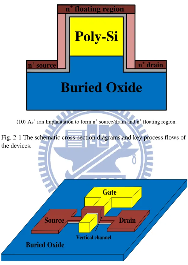
The overall fabrication process flow of the vertical thin-film-transistors (VTFTs) is shown in Fig 2.1.
First of all, the 550-nm thick thermal oxide was grown on Si wafer as starting substrate. Then 200-nm thick poly-Si layer was deposited for gate by low-pressure chemical vapor deposition (LPCVD) system using SiH4 as source gas. The gate was
implanted with phosphorous, the energy and the dose of the implantation were 40 keV and 5 × 10¹⁵ 𝑐𝑚−2, respectively. Subsequently, the dopants were activated by furnace
at 600 oC for 24 hours.
After the gate patterning, the oxide was overetched to about 80-nm to form the offset region. Then, the 15-nm thick layer of tetraethoxysilane (TEOS) oxide and 50-nm thick undoped amorphous Si (a-Si) layer were deposited consecutively as gate oxide and active region by LPCVD. The deposition pressure and temperature of a-Si film are 350 mTorr and 560 oC, respectively. After active region patterning, Ni-window
mask pattern was form on the top of the TFTs using photoresist. The 10-nm Ni film was deposited by electron-beam evaporation system and then Ni film on the photoresist was removed by the lift-off process. Ni contacts with a-Si only in the seeding window; other areas of wafers outside the seeding window are mostly free of Ni contamination. We used two methods to complete the channel crystallization: MILC and NSILC. The MILC-VTFTs were fabricated without Ni-silicidation process by rapid thermal annealing (RTA). In the NSILC-VTFTs, the Ni-silicidation was carried out at 450 oC
13
solution at 120 oC for 10 min. Next, both devices were crystallized subsequently at 500
o
C for 48 hours in N2 ambient.
Then, a 15-nm thick TEOS oxide was deposited and 15-keV, 5 × 10¹⁵ 𝑐𝑚−2 As+ ion implantation to form self-aligned n+ S/D and n+ floating region. Then the dopants
were activated by RTA at 750 oC for 30 s. The three-dimensional graph of the device
structure is shown in Fig. 2-2.
2.1.2 Fabrication results
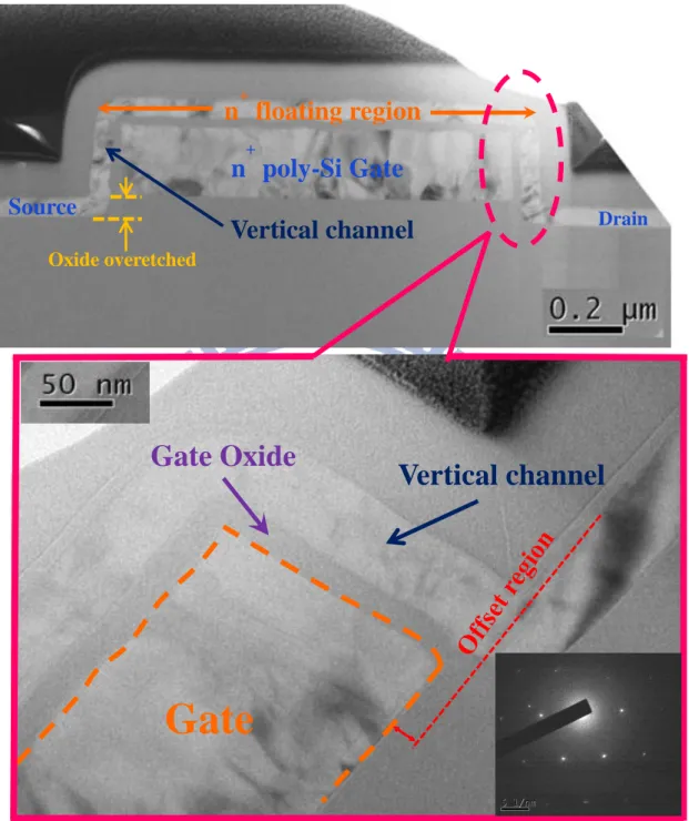
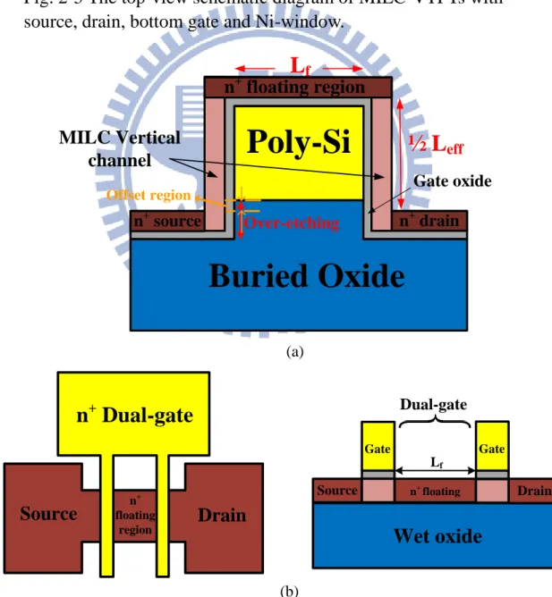
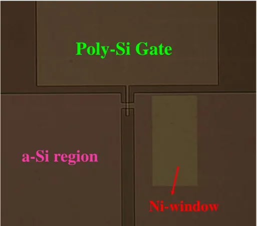
Fig. 2-3 and Fig. 2-4 show the cross-sectional transmission electron microscope (TEM) microphotograph of the NSILC-VTFTs and MILC-VTFTs. The integrity of the vertical poly-Si channel is verified by the transmission electron diffraction (TED) pattern inserted in TEM microphotograph. In the TEM images, the gate oxide and the poly-Si thickness in the channel are roughly 20-nm and 50-nm, respectively. The offset region between the gate and the S/D edges was achieved by wet-oxide overetched resulting in about 20-nm offset region. Fig. 2-5 displays the top-view schematic diagram of MILC-VTFTs with source, drain, bottom gate and Ni-window. And the schematic cross-sectional view and effective dual gate structure of MILC-VTFTs are shown in Fig. 2-6. The length of floating n+ region (Lf) is defined by the mask channel
length, and the mask channel width (Wmask) is equal to the effective channel width. The
effective channel length Leff is the vertical channel region, which is defined as 2 × the
total thickness of the poly-Si gate, which equals 0.4 μm. Moreover, the equivalent dual-gate structure can reduce the peak lateral electrical field in the drain depletion region, significantly reducing the leakage current and increasing the Ion /Ioff current ratio
[1]-[2].
The Fig. 2-7 shows optical microscopy photograph of active pattern with the source, the drain, channels, bottom-gate and Ni-seeding window. The gate length is 1
14
μm, and the channel width is 2 μm. The optical micrograph of a sample heat treated for 3 h at 500 °C, as in Fig. 2-8(a), the crystallization was seen to proceed laterally from the Ni-window and the MILC distance was around 5.98 μm from the Ni-seeding window. And the crystallization was completed in 12 h as in Fig. 2-8(b), the whole active channel was crystallized by the MILC process. Three distinct regions are visible: the rectangle with the brighter contrast was originally covered by Ni, which is MIC region. This is surrounded by the MILC region with the brightest contrast. And the darkest area in the out of MILC region is a-Si region. These results indicate that the active channel can be crystallized during the MILC process at 500 oC for 48 hours.
2.2 Method of Device Parameter Extraction
In this thesis, all of the electrical properties of proposed poly-Si TFTs were measured by semiconductor characterization system Keithley 4200. Many methods have been proposed to extract the characteristics of poly-Si TFT. In this section, extractions of various electrical parameters are introduced. These parameters include the subthreshold swing (S.S.), Filed-effect mobility (𝜇𝑒𝑓𝑓), On-state current (Ion), and Off-state current (Ioff).
2.2.1 Determination of Subthreshold swing
Subthreshold swing (S.S.) is an important parameter to describe the control ability of gate toward the channel, reflecting the switch speed of the device. It is defined as the amount gate voltage required to increase/ decrease drain current by one-order of magnitude. In general, the S.S. should be independent on drain voltage and gate voltage. However, there are many non-ideal effects in MOSFETs and TFTs. The degradation of the S.S. with increasing drain voltage is due to short channel effect, avalanche multiplication, and punch through effect. Moreover, the subthreshold swing
15
is related to gate voltage which attributes the undesirable factor, such as interface states and gate oxide thickness.
In this thesis, the S.S. is defined as a quarter of gate voltage required to increase drain current by four-orders of magnitude.
S. S. ≡ 𝜕𝑉𝐺
𝜕(𝑙𝑜𝑔𝐼𝐷)= (𝑙𝑛10) 𝜕𝑉𝐺
𝜕(𝑙𝑛𝐼𝐷)
By neglecting the depletion capacitance in the active layer, Takashi Noguchi has reported that effective interface-trap-state-density (Nit) near the poly-Si/ SiO2 interface
can be extracted from the subthreshold swing [3]-[5]. 𝑁𝑖𝑡 = [( 𝑆. 𝑆. 𝑙𝑛10) ( 𝑞 𝑘𝑇) − 1]( 𝐶𝑜𝑥 𝑞 )
2.2.2 Determination of Field Effect Mobility
Usually, the field effect mobility (𝜇𝑒𝑓𝑓) is extracted from the maximum value of transconductance (gm) at low drain voltage (VDS = 0.1 V, VGS-Vth >> VDS ). The transfer characteristic of poly-Si TFTs is similar to traditional MOSFET, so the first order of I-V relation in the bulk Si MOSFETs can be applied to poly-Si TFTs. The drain current in linear region (VD < VG – Vth) can be approximated as the following equation:
𝐼𝐷 = 𝜇𝑒𝑓𝑓𝐶𝑜𝑥(
𝑊
𝐿) [(𝑉𝐺𝑆− 𝑉𝑡)𝑉𝐷𝑆− 1 2𝑉𝐷𝑆2]
Where W and L are channel width and channel length, respectively. Cox is the gate
oxide capacitance per unit area and the Vth is the threshold voltage. Thus, the
transconductance gm is given by
𝑔𝑚 = 𝜕𝑉𝜕𝐼𝐷
𝐺|𝑉𝐷𝑆=𝑐𝑜𝑛𝑠𝑡. = 𝜇𝑒𝑓𝑓𝐶𝑜𝑥(
𝑊 𝐿)𝑉𝐷𝑆
Therefore, the field-effect mobility is obtained by
𝜇𝐹𝐸 = 𝐿
16
2.2.3 Determination of ON/ OFF current ratio
On/off current ratio is one of the most important parameters of poly-Si TFTs. An promising poly-Si TFT technique should not only provides high on-state current but also low off-state leakage current. For switching elements, as pixel cell, the off state is frequently operated in normal operation. Therefore, on/off current ratio is evidently a more appropriate evaluation parameter compared with on state current alone. The leakage current mechanism in the poly-Si TFTs is more complicated than single crystal device. For single crystal device, the channel film is composed of single crystalline and the leakage current is due to the tunneling of minority carrier from drain region to accumulation layer located in channel region. However, in poly-Si TFTs, the channel is composed of poly-Si grain, which has lots of inherence defects in the intra-grain and inter-grain site. And most of the density of states located within deep state close to the middle of the forbidden band-gap, and increase as the number of dangling bond increases. Thus, the leakage current due to trap-assisted tunneling and band-to-band tunneling is much larger in poly-Si TFTs than in the single crystal MOSFETs.
In this thesis, the on-state current is defined as the drain current when the gate voltage at 6V and drain voltage is 0.1V for n-channel TFT. The off-state current is defined as the minimum current when the drain voltage equals to 0.1V.
𝐼𝑜𝑛
𝐼𝑜𝑓𝑓 =
𝐷𝑟𝑎𝑖𝑛 𝑐𝑢𝑟𝑟𝑒𝑛𝑡 𝑜𝑓 𝐼𝐷𝑆−𝑉𝐺𝑆 𝑝𝑙𝑜𝑡 𝑎𝑡 𝑉𝐷𝑆=0.1 𝑉,𝑉𝐺𝑆=6𝑉
17
Buried Oxide
Poly-Si
(1) 550-nm thick buried oxide was grown and 200-nm a-Si was deposited.
Buried Oxide
Poly-Si
Phosphorous implant
(2)
Phosphorous implantation.
Buried Oxide
n
+
poly-Si
18
Buried Oxide
Poly-Si
Ni
Buried Oxide
Poly-Si
(4) Dry etching the poly-Si and 80-nm thick buried oxide to define the gate pattern.
Buried Oxide
Poly-Si
a-Si
(5) Deposit the 15-nm thick TEOS oxide and 50-nm thick a-Si as gate oxide and channel respective.
19
Poly-Si
Buried Oxide
Ni
(7)
The Ni film on the photoresist was removed by the lift-off process.Poly-Si
Buried Oxide
NiSi
(8) The Ni-silicide was formed at 450 ℃ for 30 s by RTA.
Poly-Si
Buried Oxide
Poly-Si channel
20
Poly-Si
Buried Oxide
n
+source
n
+drain
n
+floating region
(10) As+ ion Implantation to form n+ source/drain and n+ floating region.
Fig. 2-1 The schematic cross-section diagrams and key process flows of
the devices.
Source
Gate
Drain
Buried Oxide
Drain
Vertical channel21
n
+floating region
Vertical Channel
n
+poly-Si Gate
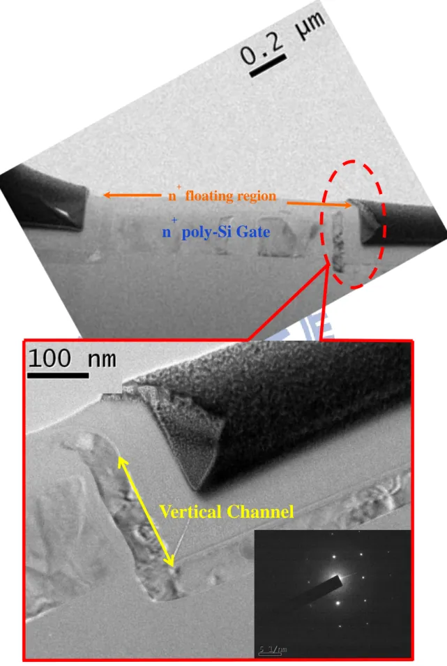
Fig. 2-3 The cross-sectional transmission electron microscope (TEM)
microphotograph and TED pattern of the NSILC-VTFTs.
22 Drain
Source
n
+poly-Si Gate
Vertical channel
n
+floating region
Oxide overetchedGate
Gate Oxide
Vertical channel
Fig. 2-4 The cross-sectional transmission electron microscope (TEM)
microphotograph and TED pattern of the MILC-VTFTs.
23 (b)
Fig. 2-6 (a) The cross-sectional schematic diagram of MILC-VTFTs and
(b) Effective dual gate structure of MILC-VTFTs.
Wet oxide
Drain Source n+ floating Dual-gate Gate Gate LfDrain
Source
n + floating regionn
+Dual-gate
Source DrainGate
Ni window Lf WmaskPoly-Si
Buried Oxide
n+ source n+ drainn
+floating region
MILC Vertical
channel
Over-etching Gate oxideL
f½ L
eff Offset regionFig. 2-5 The top-view schematic diagram of MILC-VTFTs with
source, drain, bottom gate and Ni-window.
24
Ni-window
Poly-Si Gate
a-Si region
Fig. 2-7 Optical microscopy photograph of active pattern with the
source, the drain, channels, bottom-gate and Ni-seeding window.
25
(a)
(b)
Fig. 2-8 The OM micrographs of a sample heat treated for (a) 3 h and (b) 12 h
of heat treatment at 500
oC, and the whole active channel was crystallized by
the MILC process.
26
Chapter 3
Characteristics of Vertical Channel Low Temperature
Nickel Induced Lateral Crystallization Poly-Si TFT
Poly-Si TFTs have attracted considerable interest due to their wide applications, such as driving pixels and peripheral circuits in AMOLEDs and system on panel (SOP). The most widely employed methods for poly-Si formation are solid-phase crystallization (SPC), excimer laser annealing (ELA) and metal-induced lateral crystallization (MILC). The a-Si thin films could be crystallized at a low temperature of below 500 oC by MILC, and it has uniform poly-Si films and low-cost production.
However, there are many intra-grain defects in poly-Si and the Ni and NiSi2
precipitates are trapped in poly-Si grain boundaries. Both Ni and NiSi2 act as trap sites
for high leakage current at the junction boundary and as scattering sources that considerably reduce the filed-effect mobility. Therefore, Ni contamination inside the MILC poly-Si film should be reduced to improve the device performance.
In order to alleviate adverse effects to obtain high performance TFTs, plasma treatment and crystal filtering can be used to produce the uniform crystal orientation and enhance the device performance. Besides, several methods have been proposed to reduce the amount of undesired metal impurity [47]-[49]. But these methods are complicated and need extra process. Accordingly, we propose a more simple method to reduce the Ni and NiSi2 contamination in the MILC region and expect the applicability
27
3.1 Effects of post treatment
It is well known that the grain boundaries exert a profound effect on device characteristic, because the charges trapped within grain boundaries and build up potential barriers to the flow of carrier subsequently. Moreover, the numerous intra-grain defects in poly-Si channel film also adversely influence on the device performance. Thus, poly-Si TFTs exhibit poor performance such as low mobility, large subthreshold swing, large threshold voltage, and large leakage current than the single-crystal counterparts. To obtain high performance poly-Si TFTs, both the grain enlargement techniques [1]-[2] and defect passivation processes have become increasingly important. In order to reduce the trap state densities in the poly-Si channel film, it can be performed by plasma treatment, including H2, O2, N2, and NH3 plasma
[3]-[7]. Traditionally, H2 plasma has been a very effective and popular method for
passivation. However, it had been observed that the introduction of hydrogen would degrade the reliability due to the weak Si-H bonds. To attenuate the hot-carrier degradation and obtain comparable device performance, NH3 anneal and NH3 plasma
passivation have been recently proposed, and the better hot-carrier reliability than using H2 plasma passivation has been realized.
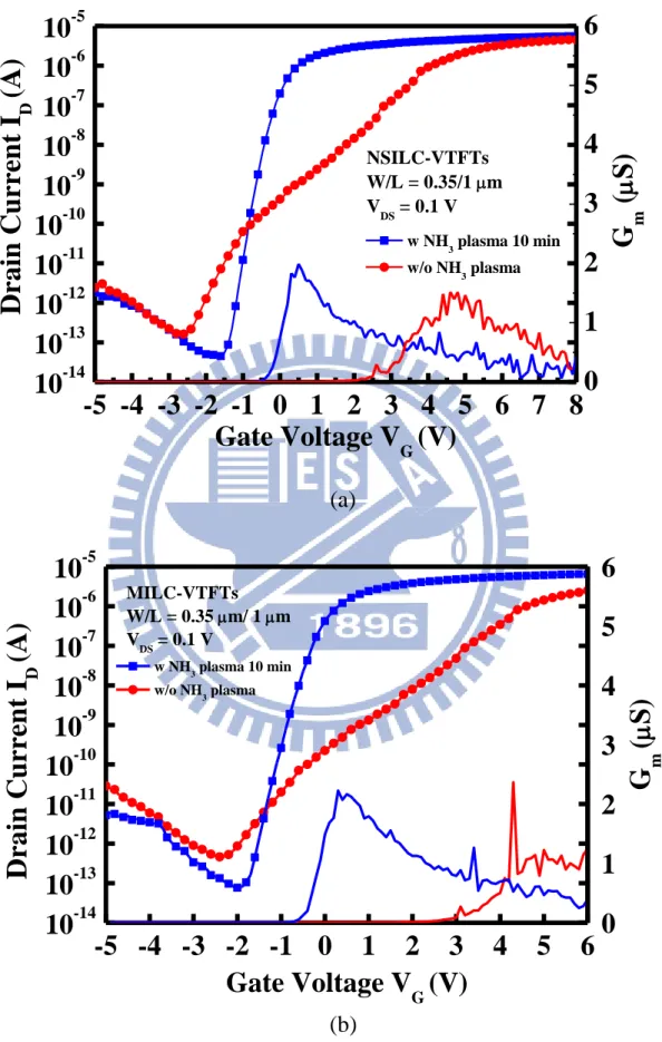
In this thesis, the NH3 plasma treatment was performed for 10 min at 300 oC with
RF power of 50 W. The flow-rate was 100 sccm at pressure of 67 Pa. The typical transfer characteristic and the transconductance of NSILC-VTFTs and MILC-VTFTs with and without NH3 plasma treatment is shown in Fig. 3-1. The length of the floating
region and channel width is 0.35 μm and 1 μm respectively.
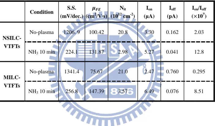
Accordingly, the subthreshold swing (S.S.) and the effective interface trap-state density (Nit) of the NH3 plasma-treated NSILC-VTFT are 224.1 mV/dec. and
2.98 × 10¹² 𝑐𝑚−2, respectively, which are superior to 1206.9 mV/dec. and 20.8 ×
1012 𝑐𝑚−2 of the control NSILC-VTFT. And the S.S and the N
28
MILC-VTFT are 256.8 mV/dec. and 3.57 × 10¹² 𝑐𝑚−2, respectively. Moreover, the
field-effect mobility of NILC-VTFT and MILC-VTFT with NH3 plasma treatment for
10 min are 131.87 cm2/V-s and 147.39 cm2/V-s, respectively. It is evident that device
characteristics are significantly improved by NH3 plasma passivation. Detailed device
parameters such as field-effect mobility (μeff), subthreshold swing (S.S.), effective
interface trap-state density (Nit), off-state current (Ioff), ON/OFF current ratio are
summarized in Table 3-1. It has higher field mobility, higher ON/OFF current ratio, lower threshold voltage, and steeper subthreshold swing with NH3 plasma treatment.
The previous study had reported that the threshold voltage and subthreshold swing are related to the dangling-bond deep trap states. They have faster response to the plasma passivation. And the leakage current and field-effect mobility, which are related to strain-bond tail trap states of poly-Si channel, have slower improvement to plasma passivation [8]. NH3 plasma passivation further improves the performance of these
devices, suggesting that the NH3 plasma effectively passivated the dangling bonds at
the grain boundary by the H and N radicals coupling and the nitrogen pile up at the SiO2/poly-Si interface resulting in the formation of strong Si-N bonds[6]-[8]. Moreover,
the NH3 plasma passivation reduces the barrier height (EB) of the poly-Si grain
boundary, the electrons can easily overcome EB, producing a high current and allowing
the TFT to be easily turned on.
3.2 Crystal Filtering Effect
The poly-Si TFTs have attracted much attention for driving pixels and peripheral circuits in AMOLEDs, due to their higher carrier mobility than a-Si TFTs. However, the presence of poly-Si grain boundary defects in the channel region of TFTs drastically influences on the electrical characteristics [9]-[10]. Therefore, the control of the orientation of the Si crystal grains enables us to control the alignment of grain
29
boundaries. Thus, the electrical performance can be improved by reducing the grain boundary defects and the randomly oriented grain boundaries from the device area. In this section, we propose the VTFTs with various crystal filter widths and multichannel structure to improve the electrical characteristics by crystal filtering effect.
In this thesis, the devices can be divided into two groups, EW2 and EW1, according to their effective widths listed in Table 3-2. The top view optical microscope microphotographs of MILC-VTFTs with various widths of crystal filter are shown in Fig. 3.2. The effective width of EW2 and EW1 are 2 μm and 1 μm respectively. Both the devices of the floating region length (Lf) were fixed at 1 μm. In the group EW2,
one with crystal filter width of 2 μm and a single-channel (designed “W2C1”), one with crystal filter width of 1 μm and two channels (designed “W1C2”), one with crystal filter width of 0.5 μm and four channels (designed “W0.5C4”), and the other with crystal filter width of 0.4 μm and five channels (designed “W0.4C5”). In the group EW1, one with crystal filter width of 1 μm and a single-channel (designed “W1C1”), and another with crystal filter width of 0.5 μm and two-channels (designed “W0.5C2”).
Fig. 3.3 shows the transfer characteristics of MILC-VTFTs with various widths of crystal filter. Compared with W2C1, W1C2, W0.5C4, W0.4C5 has better device performance than its counterparts. Moreover, the W0.5C2 also has the significant performance than other. These results indicate that the narrower the unit channel width is, the better the electrical performance is, including higher on-state current, steeper subthreshold swing, and lower off-state current. This is attributed to that lower probability of the channel region covers the grain boundary in narrower width devices and the channel region would have more uniform crystal growth direction than the unfiltered active layer of MILC-VTFT area. The narrower the widths of the crystal filters are, the more uniform the crystallographic orientation the MILC poly-Si is
30
[11]-[12]. In general, the c-Si grains grow toward the a-Si region with the migration of NiSi2 and the individual crystallites form networks in Ni-MILC process. Moreover, if
the NiSi2 layer at the front of c-Si grain meets other crystal grains crystallized by the
MILC process. Subsequently, the NiSi2 cannot migrate through the c-Si anymore
because there is no difference of chemical potential driving force for the phase transformation between the two c-Si grains [13]. Therefore, the captured NiSi2 would
increase silicide contaminations in the MILC region. For the crystal filtering method, there are few crystal Si grains, which has growth direction parallel to the crystal filter, can pass through the filter. Thus, the crystallized Si grains have longer grain lengths, similar crystal orientation and dense microstructure could be selected through crystal filter [14]-[15]. Therefore, the narrower crystal filter width has better grain crystallization, less intra-grain defects, less grain boundaries defects and NiSi2
contaminations in the poly-Si channel. Hence, the device performance, including higher on-state current, steeper subthreshold swing, lower off-state current, will be improved by reducing the crystal filter width.
In order to further confirm the crystal filter effect is correct, we measured more than 20 devices to determine the statistical average values of on-state current (Ion),
off-state current (Ioff ), subthreshold swing (S.S.), and transconductance (Gm) of group
EW2 and EW1, shown in Fig. 3-4 – Fig. 3-11. Based on the statistical result, the narrower crystal filter width also has higher Ion, lower Ioff, steeper S.S., and higher Gm
than others wider crystal filter width. The statistical average values of some important parameters of all devices are summarized in Table 3-3. The W0.4C5 also has the highest field-effect mobility (μFE) as 87.5 cm2/V·s in the group EW2. And the W0.5C2
has the best field-effect mobility as 96.3 cm2/V·s in all devices. These results were
similar to previous reports, indicating that the poly-Si grain lateral length increase as the channel width declines and the grain boundary defects of poly-Si would be reduced
31 to increase the mobility.
In addition, the longitudinal grains and their boundaries are parallel to the direction of carrier flow in the channel. The wide channel devices with grain boundaries traversing from source to drain provide extra current paths and cause punchthrough. However, the VTFTs inherently own an effective dual gate structure and the offset region, constructed by self-aligned oxide overetching. The previous study had reported that the OFF-state currents can be improved by increasing the oxide overetching depth and equivalent dual-gate structure [16]. This improvement on leakage current originates from reducing the lateral electrical field in the drain depletion region [17]-[20]. Thus, the OFF-state current of these device can be reduced below 1 pA/ μm.
3.3 Compare NSILC-VTFT with MILC-VTFT
According to the previous report [21], the excess Ni accumulation in the middle of the n+ floating region is found in the MILC-VTFTs, but it is not found in the NSILC-VTFTs. The Ni and NiSi2 precipitates trapped in the grain boundary would act
as trap sites which increase the leakage current and degrade the field-effect mobility.
In this section, we focus on discussing the different electrical characteristics
between NSILC-VTFTs and MILC-VTFTs. Fig. 3-12 –Fig. 3-15 show the on-state current distribution, off-state current distribution, subthreshold swing distribution, and transconductance distribution of the NSILC-VTFTs and MILC-VTFTs with 1 μm of length of n+ floating region and channel width from 0.35 μm to 1 μm, respectively. We
can observe that the electrical performance of NSILC-VTFTs and MILC-VTFTs seems to be no significantly difference. No matter what size of device we choose, we still have the same conclusion: There are no difference between NSILC-VTFTs and MILC-VTFTs.
32
This observation can be possibly ascribed to the following explanations. In this work, we used the unilateral crystallization method to complete the channel crystallized. Therefore, there is no excess Ni accumulation found in MILC-VTFTs and NSILC-VTFTs. And the MILC/MILC grain boundary in the middle of the channel can be eliminated. If the Ni content is provided by an appropriate amount to complete the channel crystallization, even MILC-VTFTs will be no excess Ni remaining in the channel. Therefore, the NSILC-VTFTs with Ni-silicided seeding window to limit the Ni source is not able to further improve the device characteristics. Nevertheless, the leakage current still can be suppressed by the dual-gate structure and offset region due to reducing the lateral electrical field in the drain depletion region.
Moreover, as channel widths decrease, the Ioff suppresses and the Gm, S.S. and Ion
enhances. These results reflect the crystal filtering once more. The average values of some important parameters are summarized in the Table 3-4. The narrower the widths of the crystal filters are, the more uniform the crystallographic orientation the MILC poly-Si is. Thus, the high performance device can be achieved by reducing the channel widths.
Although the narrower the channel width is the better the electrical performance, the on-state current would be degrade due to the W/L factor reducing. In order to overcome this problem, we proposed a layout which given high performance VTFTs. The design of wide devices usually involves the breakdown of a wide transistor into a number of smaller transistors in parallel. In this experiment, we fabricated the multiple channels structure, which unit channel width of 0.35 μm. Fig. 3-16 shows the transfer characteristics of a MILC-VTFT with unit crystal width of 0.35 μm under various channel number. These results indicate that the multiple channel and crystal filtering effect can significant improve the on-state current, while maintaining the high performance of VTFTs. When the channel numbers are increased, the S.S. still remains
33
better performance about 300 mV/dec.. Moreover, the off-state current can significantly be reduced with both the equivalent dual-gate structure and offset region, and the on-state current and Gm can evidently be improved by multiple channels. In
order to further verify the result is correct, more than 20 devices are measured to obtain the statistics. The average values of some important parameters such as Ion, Ioff, S.S.,
Gm and their standard deviations with unit crystal width of 0.35 μm for various channel
number are shown in Fig. 3-17- Fig. 3-20. As a result, the combination of narrower crystal width and multiple channels can successfully further optimize electrical characteristics of poly-Si TFTs, owning to the elimination of grain boundaries and defects.
34
Fig. 3-1 The typical transfer characteristic and the field-effect mobility of
(a) NSILC-VTFTs and (b) MILC-VTFTs with and without NH
3plasma.
treatment.
(a)
(b)
-5 -4 -3 -2 -1 0 1 2 3 4 5 6 7 8
10
-1410
-1310
-1210
-1110
-1010
-910
-810
-710
-610
-5G
m(
S
)
w NH 3 plasma 10 min w/o NH 3 plasma NSILC-VTFTs W/L = 0.35/1 m VDS = 0.1 VDra
in Curre
nt
I
D(A
)
Gate Voltage V
G(V)
0
1
2
3
4
5
6
-5 -4 -3 -2 -1 0
1
2
3
4
5
6
10
-1410
-1310
-1210
-1110
-1010
-910
-810
-710
-610
-5G
m(
S
)
Dra
in Curre
nt
I
D(A
)
Gate Voltage V
G(V)
w NH3 plasma 10 min w/o NH3 plasma0
1
2
3
4
5
6
MILC-VTFTs W/L = 0.35 m/ 1m VDS = 0.1 V35 Condition S.S. (mV/dec.) 𝝁𝑭𝑬 (cm2/V∙s) Nit (1012 cm-2) Ion (μA) Ioff (pA) Ion/Ioff (×107) NSILC-VTFTs No-plasma 1206. 9 100.42 20.8 3.30 0.162 2.03 NH3 10 min 224.1 131.87 2.98 5.27 0.041 12.8 MILC-VTFTs No-plasma 1341.4 75.67 21.0 2.47 0.760 0.295 NH3 10 min 256.8 147.39 3.57 6.49 0.076 8.51
Table 3-1 Characteristics of poly-Si TFTs with and without plasma
treatment. All parameters are extracted at V
d= 0.1 V. W/L = 0.35 μm/ 1 μm
36
Group
Device
Unit channel
Total
channel
width
width
number
EW 2
W2C1
2
1
2 μm
W1C2
1
2
W0.5C4
0.5
4
W0.4C5
0.4
5
EW 1
W1C1
1
1
1 μm
W0.5C2
0.5
2
37
W2C1
W 1C2
W0.5C4
W0.4C5
W1C1
W0.5C2
(b)
Fig. 3-2 The top view optical microscope microphotograph of MILC-VTFTs
with various widths of crystal filter. (a) Total width = 2 μm (b) Total width =1μm
38 W2 C1 W1 C2 W0.5 C4 W0.4 C5
-4 -3 -2 -1
0
1
2
3
4
5
6
10
-1410
-1310
-1210
-1110
-1010
-910
-810
-710
-610
-510
-4Drain curre
nt
I
DS(A)
Gate voltage V
G(V)
MILC-VTFTs Lf = 1 m VDS = 0.1 V NH3 plasma 10 min Effective width = 2m(a) Effective widths = 2 μm
W1 C1
W 0.5 C2
-4 -3 -2 -1
0
1
2
3
4
5
6
10
-1410
-1310
-1210
-1110
-1010
-910
-810
-710
-610
-510
-4Drain
curr
ent
I
DS(A)
Gate voltage V
G(V)
MILC-VTFTs L f = 1 m V DS = 0.1 V NH 3 plasma 10 min Effective width = 1 m(b)
Effective widths = 1 μm
Fig. 3-3 The transfer characteristics of MILC-VTFTs with various widths
of crystal filter. (a) Effective widths = 2 μm (b) Effective widths = 1 μm
39

![Fig. 1-4 Schematic of the growth mechanism of Ni-induced lateral crystallization [36]](https://thumb-ap.123doks.com/thumbv2/9libinfo/8748566.205406/25.892.173.738.421.1072/fig-schematic-growth-mechanism-ni-induced-lateral-crystallization.webp)