國 立 交 通 大 學
電子物理學系
博 士 論 文
非對稱金氧半場效電晶體及無接面多晶矽薄膜電晶
體的研究
A Study on Asymmetrical MOSFETs and Junctionless
Polycrystalline Silicon Thin-Film Transistors
研 究 生:蔡子儀
指導教授:趙 天 生 博士
林 鴻 志 博士
黃 調 元 博士
非對稱金氧半場效電晶體及無接面多晶矽薄膜電晶
體的研究
A Study on Asymmetrical MOSFETs and Junctionless Polycrystalline
Silicon Thin-Film Transistors
指導教授:趙天生 博士
Advisors:Dr. Tien-Sheng Chao
林鴻志 博士
Dr. Horng-Chih Lin
黃調元
博士
Dr.
Tiao-Yuan Huang
研 究 生:蔡子儀
Student:Tzu-I Tsai
國 立 交 通 大 學
電子物理學系
博士論文
A DissertationSubmitted to Department of Electrophysics College of Science
National Chiao Tung University in Partial Fulfillment of the Requirements
for the Degree of Doctor of Philosophy
in Electrophysics December 2013
Hsinchu, Taiwan, Republic of China
非對稱金氧半場效電晶體及無接面多晶矽薄膜電晶體
的研究
研究生:蔡子儀 指導教授:趙天生 博士
林鴻志 博士
黃調元 博士
國立交通大學
電子物理學系
摘 要
在本論文中,我們利用傳統 I-line 步進機發展一新穎雙重微影技術,可將閘極 長度微縮至 80 奈米;而後改良此雙重微影製程可進一步縮小其線寬以製作出次 60 奈米線寬圖形,並將之用於 45 奈米 n 型通道金氧半場效電晶體的製作。此技術與 一般大學實驗室常用的方法,例如電子束直寫系統與光阻灰化技術進行比較,包 括臨界尺寸(CD)均勻性、產率、線邊緣粗糙度(LER)、最小線寬等特性,作定量上 的比較。憑藉所提出的 I-line 雙重微影技術,我們也研製出對稱與非對稱源汲極元 件,並討論其電性特性與相關的可靠度議題。 我們發現,雖然對稱暈邊(halo)結構相較於對照組能有效降低 104倍次臨界漏 電及改善短通道效應,但同時造成嚴重的逆短通道效應與犧牲 25%電流驅動力。 為了改善這項缺失,我們提出非對稱暈邊結構製程以解決上述的矛盾。相較於對 稱暈邊結構,非對稱暈邊結構貢獻了 7.8% 的轉導增益以及 15%電流驅動力增益 另外在可靠度議題方面,我們發現暈邊掺雜會增加在閘極邊緣下汲極的側向電場 強度,進而使熱載子退化效應變得更嚴重。藉由非對稱暈邊結構,我們可以減緩 熱載子退化效應,其臨界電壓偏移為 0.21 伏特,對稱式結構則為 0.32 伏特的臨界 電壓偏移。此外,我們也藉由探討熱載子測試前後的閃爍雜訊特性來評估暈邊掺 雜對元件的影響,發現汲極端暈邊掺雜也會造成元件雜訊劣化。 另一方面,我們研製出各式不需佈植製程的無接面元件,包含多閘極組態奈米線場效電晶體、三維多層堆疊奈米線場效電晶體、多閘極組態奈米線 SONOS 記 憶體元件、以及平面式薄膜電晶體以探討其操作機制。藉由導入臨場磷摻雜多晶 矽薄膜作為上述無接面元件的通道及源汲極材料以實現無佈植技術的製程方式。 由無接面奈米線場效電晶體的電性結果發現,足夠小的奈米線通道截面對於關閉 n 型重摻雜通道與得到優異電流開關比值(在閘極電壓為 2 伏特下有 5.2 × 10⁶倍)是 非常重要的。此外,由於較低的源汲極串聯阻值與通道阻值,無接面元件具有較 高的電流驅動表現約為反轉式元件的 1.75 倍。 接下來,相較於反轉式元件而言,無接面奈米線 SONOS 記憶體元件展現較快 的寫入速度與不錯的資料保存能力,而相當的抹除速度與毫不遜色的記憶窗口也 被記錄。另一方面,摻雜濃度與閘極組態對於無接面記憶體元件的效應也一併探 討。由電性與記憶體特性結果發現對於高性能 SONOS 應用方面而言,無接面多晶 矽奈米線記憶體元件的摻雜濃度必須謹慎的調整。簡而言之,就低成本與極高密 度非揮發記憶體應用而言,所提出的無接面奈米線 SONOS 技術是相當有潛力的。 最後,我們研製 n 型平面式超薄型無接面多晶矽薄膜電晶體以探討對射頻與 低頻雜訊之影響。在汲極電壓 2 伏特偏壓下無接面元件展現出優異的截止頻率(3.36 GHz)與最大共振頻率(7.37 GHz)以實現低電壓操作的應用。在低頻雜訊方面,相較 於對照組的反轉式元件,無接面元件改善了低頻雜訊以及達到較高的信號雜訊 比。此外,我們也建立了無接面元件的小訊號模型並且對照實驗與模擬結果以驗 證其準確性,由對照的結果發現所建立的小訊號模型是成功運作的。
A Study on Asymmetrical MOSFETs and Junctionless
Polycrystalline
Silicon Thin-Film Transistors
Student:Tzu-I Tsai Advisors:Dr. Tien-Sheng Chao
Dr. Horng-Chih Lin
Dr. Tiao-Yuan Huang
Department of Electrophysics
National Chiao-Tung University
Abstract
In this dissertation, we have developed a novel double-patterning (DP) technique for generation of gate patterns with gate length down to 80 nm using only a conventional I-line stepper. With a modification in the process steps, this DP technique can further shrink the patterns down below sub-60 nm and have been employed to fabricate 45nm nMOSFETs. This technique is also compared with alternative methods, such as electron-beam direct writing and photoresist-ashing scheme which are often adopted in the university-based laboratories, from the perspectives of the uniformity of critical dimension (CD), throughput, line edge roughness (LER), and minimum line width. Moreover, with the aid of the proposed I-line DP technique, several symmetrical or asymmetrical S/D devices were fabricated and characterized.
We found that, although the symmetrical halo-doping structure helps reduce the subthreshold leakage by four orders of magnitude over the control and improve the short-channel effects (SCEs), severe reverse-short-channel effect (RSCE) and degenerate current drivability (25% output current degradation as compared with the control) are compromised at the same time. To address this issue, the implementation of asymmetrical halo structure was proposed to relieve such a dilemma. In contrast with symmetrical halo structure, the Asymmetric Halo split shows a 7.8% higher transconductance and a 15% larger driving current. For reliability issue, we found that the drain-side halo doping is the primary culprit of hot-carrier (HC) degradation due to the increased peak lateral electric field. The aggravation of HC degradation is alleviated with the Asymmetric Halo split, while the Symmetric Halo split exhibits threshold
voltage shift of 0.32 V and the Asymmetric Halo split performs that of 0.21 V after 5000-second of hot-electron stressing. Furthermore, we have evaluated the impact of halo on device performance by investigating the flicker noise (1/f) characteristics before and after the hot-carrier stress, indicating that drain-side halo doping. deteriorates low-frequency noise as well.
Concurrently, we have fabricated and characterized junctionless (JL) polycrystalline silicon-based thin-film transistors (TFTs) of various configuration, including multiple-gated nanowire (NW) field-effect transistors (FETs), 3-D multilayer-stacked NWFETs, multiple-gated NW silicon–oxide–nitride–oxide–silicon (SONOS) memory cells, and planar TFTs with an implant-free technique. The results indicate that a sufficiently small cross section of the channel, less than 20 nm × 20 nm, is essential to switch off the device and obtain a superior on-to-off current ratio of 5.2 × 10⁶ at VG = 2 V. Moreover, JL devices exhibit boosted on-state behavior (a 1.75 times
output current value over the inversion-mode counterpart), as ascribed to lower S/D series resistances and channel resistances.
The fabricated NW SONOS memory devices with JL scheme depict faster programming speed and better data retention behavior, while a comparable erase window and similar erasing efficiency to the inversion-mode (IM) counterparts are also observed. On the other hand, the effects of doping concentration and gate configuration implemented with JL scheme have also been investigated. From the results of the electrical characterizations and memory properties, the doping concentration of the JL poly-Si NW device should be carefully optimized for high-performance SONOS applications.
We’ve also fabricated and characterized n-type planar ultrathin JL poly-Si TFTs with emphasis on RF and low-frequency noise (LFN) performance. The 0.2-μm JL device shows remarkable ft and fmax of 3.36 and 7.37 GHz, respectively, at a VD of 2 V.
In addition, the JL devices improve the LFN and achieves higher signal-to-noise ratio as compared with those of the IM devices. Finally, we have derived a small-signal model for the fabricated JL devices and verified its accuracy by comparing the S-parameters.
Acknowledgement
首先要感謝指導教授趙天生博士、林鴻志博士與黃調元博士。三位老師在專 業領域上的知識,對於研究的熱誠,嚴慎的做事態度與強烈追求新知的精神是學 生由衷景仰與遵循的楷模。無論是日常生活或是專業研究領域,老師們常給予學 生種種的指導、教誨與關心,老師們的所有建議學生都謹記在心,於此誠摯感謝 老師們的一切付出。 本論文的完成也要感謝口試委員—胡振國教授、李明逵教授、鄭晃忠教授、 賴朝松教授、蘇彬教授授—所給予的寶貴建議與指導。 接下來我要感謝先進元件技術實驗室的所有成員在生活與實驗上所提供的各 種協助。感謝李耀仁博士、盧文泰博士、呂嘉裕博士、李明賢博士、盧景森博士、 徐行徽博士、陳威臣博士、林哲民博士、張凱翔學長、黃健銘學長等等早期辛苦 為實驗室奠定的基礎,由量測系統的建立到許多便利的量測技術以及實驗室制度 等,正所謂前人植樹後人乘涼,學弟在此由衷感謝前輩們的付出。感謝蘇俊榮博 士在奈米線元件上深厚的功力與經驗得以順利完成本論文無接面奈米線元件相關 的討論。感謝曾經一起努力熬夜爆肝做實驗與趕國科會計畫的博班夥伴們—政頤 (阿毛)、嘉豪(maca)、克慧(Kerker)、博璿(阿莫)、嘉文(Albert)、榮哲、明鴻、金儀 與你們共事是我的榮幸,還有碩士班的學弟妹們—冠樟、忠祐、政雄、漢仲、陳 玲、小強、SRJ、Gay 綸、敏峰、家維、博翔、段凱、禹伶、孝雄、廷燿、靜玲、 信宏,族繁不及備載,謝謝你們在研究實驗上的協助與生活的交流,為研究生涯增 添不少樂趣。 另外還要感謝國家奈米元件實驗室與交大奈米中心所有的工作人員,提供如 此便利與完善的環境,雖然設備有時會故障但優秀的工程師能快速的回復狀況, 使得實驗最終能夠順利的進行。感謝國家奈米元件實驗室的林家毅工程師在 FIB 上的鼎力相助、薛富國工程師在蝕刻上的協助、鄭旭君工程師在微影上的協助、 陳柏源工程師在高頻量測上的協助、陳坤明博士在 RF 相關研究的討論,以及製程 服務組的幫忙—耘木疌、明娟、家如、李姊、琇芝、婉貞、庭瑋、台鳳、子綾、 宋爺、蔣姊,即使我離開了,精神永遠與你們同在,最後一年的低潮期中感謝你 們與實驗室學弟妹的開導與鼓勵讓我完成了這本論文。最後特別要感謝我的父母親 蔡文全先生與邱昭綾女士,對我從小到大無怨無 悔的付出與照顧,該是您老享清福的時候,兒子終於能夠回饋您們的養育之恩。 感謝兩位姐姐如涵、依珊,在我求學過程中的關懷與照顧。 謹以此論文獻給我最敬愛的家人、朋友以及敬重的師長們。 蔡 子 儀 誌於風城交大 2014 年 1 月
Contents
Abstract (Chinese)……….. i
Abstract (English)………... iii
Acknowledgement (Chinese)……….. v Contents ……….. vii Table Captions ……… x Figure Captions ……….. xi Chapter 1 Introduction………... 1 1.1 General Background……… 1
1.1-1 Double Patterning Technique ……….. 1
1.1-2 Junctionless Technique………..……….. 2
1.1-3 Asymmetric S/D Devices...……….………..………... 2
1.1-4 Flicker Noise Characteristics……..…...……….. 4
1.1-5 Radio Frequency Techniques.………..……… 6
1.2 Motivation………... 7
1.3 Thesis Organization ……… 8
References ……… 11
Chapter 2 A Simple Method for Sub-100 nm Pattern Generation with I-line Double Patterning Technique……….………. 25
2.1 Introduction ……… 25
2.2 Development of Double Patterning with I-line Stepper……..……… 26
2.3 Devices Fabrication ...…...……..……… 27
2.4 Results and Discussion ………... 28
2.4-1 End Point Detection Issue ………..………. 28
2.4-2 Feasibility of Double Patterning Technique ...………. 29
2.4-3 Device Characteristics ………...………. 31
2.5 Summary ……… 33
Chapter 3 A Comparison of Nano-scale Patterning Techniques….……… 54
3.1 Introduction ……… 54
3.2 Lithographic Experiments ..……… 56
3.2-1 Brief Illustrations of Lithographic Experiments ……… 56
3.2-2 Experiments of Electron Beam Systems ……… 56
3.2-3 Experiments of I-Line Stepper with PR Ashing Method ……… 56
3.2-4 Experiments of I-Line Stepper with Double Patterning Method ………… 57
3.2-5 Experiments of I-Line Stepper with Modified Double Patterning Method. 58
3.3 Devices Fabrication ……… 59
3.4 Results and Discussion ………... 60
3.4-1 Performance Comparison of Lithographic Techniques ..……… 60
3.4-2 Devices Characteristics ………..……… 61
3.5 Summary ……… 64
References ……… 65
Chapter 4 Fabrication of Sub-100 nm Devices with Asymmetrical Source/Drain Using I-line Double Patterning Technique……….. 82
4.1 Introduction ……… 82
4.2 Devices Fabrication ……… 84
4.3 Measurement Setup ……… 86
4.3-1 Electrical Measurement Setup ………...…...……… 86
4.3-2 Hot-Carrier Stress Measurement Setup ………...……… 86
4.3-3 Charge Pumping Measurement Setup………...……… 87
4.3-4 Flicker Noise Measurement Setup………...…...……... 88
4.4 Results and Discussion ………... 88
4.4-1 Electrical Characteristics of TFETs……….……… 88
4.4-2 Electrical Characteristics of nMOSFETs………...………….. 91
4.4-3 Hot-Carrier Stress (HCS) of Asymmetrical Halo nMOSFETs…………... 93
4.4-4 Lateral Distribution of Interface Trap Density of Asymmetrical Halo nMOSFETs……….. 95
4.4-5 Flicker Noise Characteristics on Asymmetrical Halo nMOSFETs……….. 96
4.5 Summary ……… 100
Chapter 5 Fabrication and Characterization of Junctionless Devices Using an
Implant-free Technique……..………... 135
5.1 Introduction ……… 135
5.2 Device Fabrication and Experiment……… 137
5.2-1 Junctionless NWFETs ………..………... 137
5.2-2 Junctionless SONOS Nonvolatile memory Devices……….... 139
5.2-3 Three-Dimensional Multilayer-Stacked Junctionless NWFETs……..….... 140
5.2-4 Planar Junctionless TFTs………..………... 141
5.3 Measurement Setup……….………... 142
5.3-1 Electrical Measurement Setup………. 142
5.3-2 S-Parameter Measurement Setup………. 142
5.3-3 De-embedding Process……….………... 143
5.4 Results and Discussion ………... 144
5.4-1 Electrical Characteristics of Junctionless NWFETs... ……… 144
5.4-2 NVM Characteristics of JL NW SONOS Devices .……… 147
5.4-3 Electrical Characteristics of 3-D Multilayer-Stacked JL NWFETs………. 151
5.4-4 RF Characteristics and Small-Signal Modeling of Planar JL TFTs………. 152
5.5 Summary ……… 155
References ……… 157
Chapter 6 Conclusions and Suggested Future Works………. 195
6.1 Conclusions ……… 195
6.2 Suggestions for Future Work ……….. 196
References ……… 198
Vita (Chinese)……….. 199
Table Captions Chapter 2
Table 2-1 Overall implantation conditions used in the n-MOSFET fabrication. .………..……….36 Table 2-2 Overall implantation conditions used in the p-MOSFET
fabrication. .………..……….36 Table 2-3 Specifications of Canon FPA-3000i5+
Stepper. .……… ….. ……….36
Chapter 3
Table 3-1 Overall implantation conditions used in the device fabrication. ……….……...67 Table 3-2 Comparisons of electron beam tools and I-line processes…….……….…...67
Chapter 4
Table 4-1 Overall implantation conditions used in the device fabrication of TFETs. ……….………...106 Table 4-2 Overall implantation conditions used in the device fabrication of
nMOSFETs……….…………..…………...106
Chapter 5
Table 5-1 Hall measurement results of poly-Si films. ………...…162 Table 5-2 Splits of JL NW SONOS devices with various gate configuration and
channel doping. ………...………162 Table 5-3 Performance comparison of the fabricated JL and IM poly-Si TFTs with
W/L=8 μm/0.4 μm……….……...……...162 Table 5-4 Summary of the small-signal parameters of fabricated JL and IM poly-Si
Figure Captions Chapter 1
Fig. 1-1 Schematic diagram of a TFET…..………..………17
Chapter 2
Fig. 2-1 Transistor cost and scaling trend of channel length versus years for technology node [1]. ………..……….37 Fig. 2-2 Process flow of poly-Si gate formation with double patterning
technique. ……….………...37 Fig. 2-3 Mask layouts of the first (G1) and second (G2) gate patterns for defining the
gate pattern on the active region. Gate length (Lovp) of the final gate is
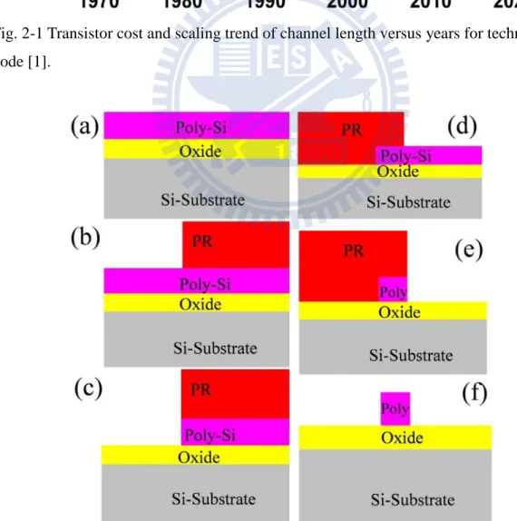
determined by the overlap region of the two gate patterns. ………..……….38 Fig. 2-4 Major process steps for fabricating n-MOSFETs with the DP method. (a)
Formation of gate oxide and poly-Si on Si wafer with LOCOS isolation. (b) Generation of first PR pattern (G1), followed by the first poly-Si etching. (c) Generation of second PR pattern (G2) after removing the first PR. (d) Completion of the poly-Si gate after second poly-Si etching and subsequent PR removal. (e) Formation of S/D structure. ………..38 Fig. 2-5 Typical optical emissive signal recorded during the main etching stage of the
second gate etching with the original mask design. No end point was detected. ………...39 Fig. 2-6 Cross-sectional SEM view of a MOSFET showing an etch-induced recess at
the right side of the gate. Top illustration is used to help visualize the structure. The recess was formed during the G2 etching stage due to the failure of EPD. ……….…39 Fig. 2-7 (a) Optical emissive signal recorded during the main etching stage of the first gate etching step with the modified mask design. ……….……….40 (b) Optical emissive signal recorded during the main etching stage of the
second gate etching step with the modified mask design. Successful EPD is achieved in the two etch steps………..40 Fig. 2-8 (a) In-line SEM views of gate patterns on active region etched with original
mask designs. The etch-induced damage region can be distinguished vividly. ……….41 (b) In-line SEM views of gate patterns on active region etched with modified mask designs. The etch recess phenomenon can be resolved with the modified mask design………..41
Fig. 2-9 Throughput of two lithography tools. ………...……….42
Fig. 2-10 Mask layout for defining the gate pattern and observed area on the active region marked with a red dashed line. ……….42 Fig. 2-11 (a) In-line SEM image of a patterned poly-Si line with nominal line width of
500 nm. The measured line width in this case is 498 nm. ……….………..43 (b) In-line SEM image of a patterned poly-Si line with nominal line width of 400 nm. The measured line width in this case is 390 nm……….43 (c) In-line SEM image of a patterned poly-Si line with nominal line width of 300 nm. The measured line width in this case is 294 nm……….44 (d) In-line SEM image of a patterned poly-Si line with nominal line width of 200 nm. The measured line width in this case is 214 nm……….44 Fig. 2-12 In-line SEM images of patterned poly-Si lines located at eight different dies of
a wafer with nominal line width of 100 nm. ……….……..45 Fig. 2-13 In-line SEM images of patterned poly-Si lines located at eight different dies of
a wafer with nominal line width of 80 nm. ……….………..45 Fig. 2-14 In-line SEM images of patterned poly-Si lines randomly located on a wafer
with nominally shortest line width of 50 nm. ………...46 Fig. 2-15 Measured poly-Si gate length (Lpoly) as a function of nominal gate length
(Lovp). ………..……….46
Fig. 2-16 Cumulative plots of poly-Si gates patterned with DP method with nominal length of 80, 300, and 400 nm, and with conventional single patterning (SP) with nominal length of 350 nm. Each curve represents the results measured from 35 test structures. ………47 Fig. 2-17 Cross-sectional SEM image of a fabricated device with nominal gate length of
120 nm. Practical length was measured to be 115 nm. ……….………..47 Fig. 2-18 (a) Transfer characteristics of NMOS control split biased at VD = 0.05V with
various channel length ranging from 0.12 to 10 μm. All devices have the same width of 10 μm. ………..…….48 (b) Transfer characteristics of NMOS control split biased at VD = 1.5V with
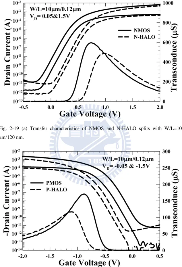
various channel length ranging from 0.12 to 10 μm. All devices have the same width of 10 μm………..……….…..48 Fig. 2-19 (a) Transfer characteristics of NMOS and N-HALO splits with W/L=10
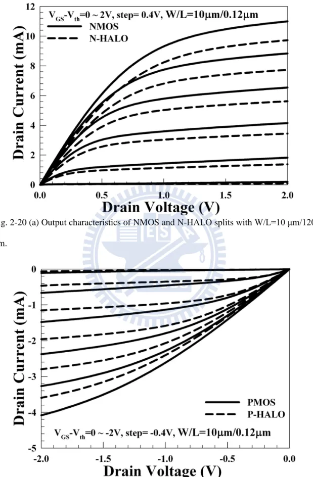
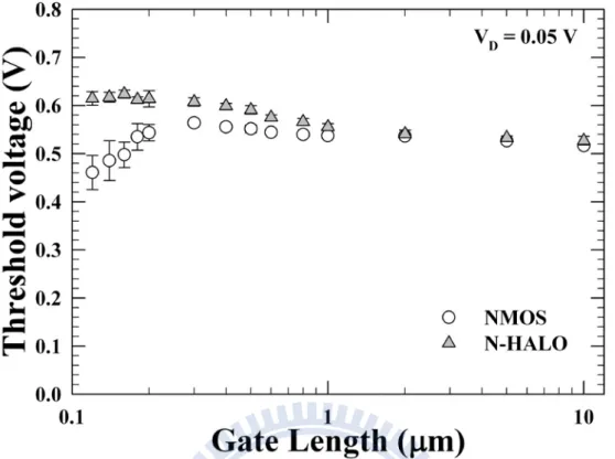
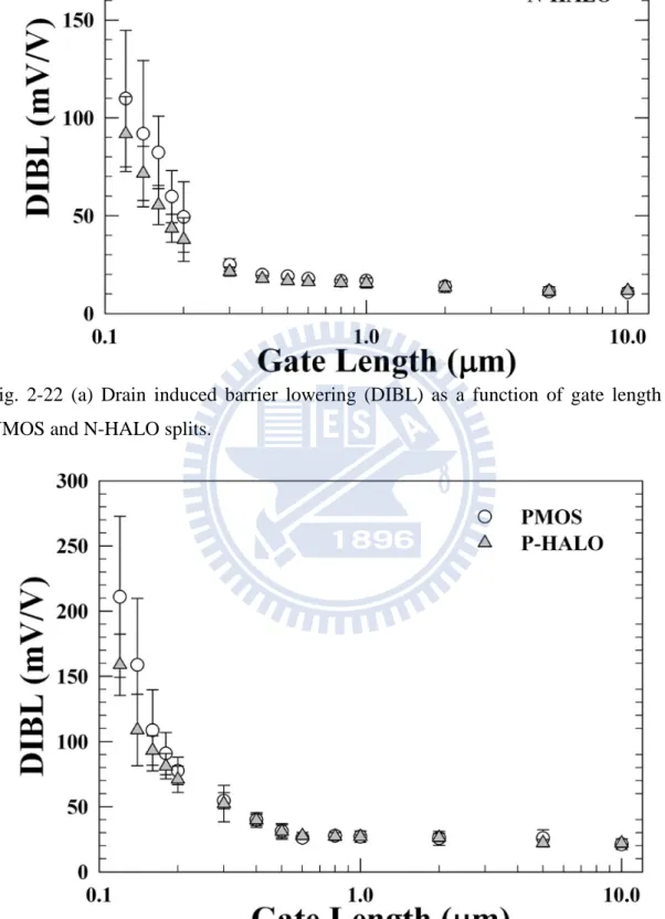
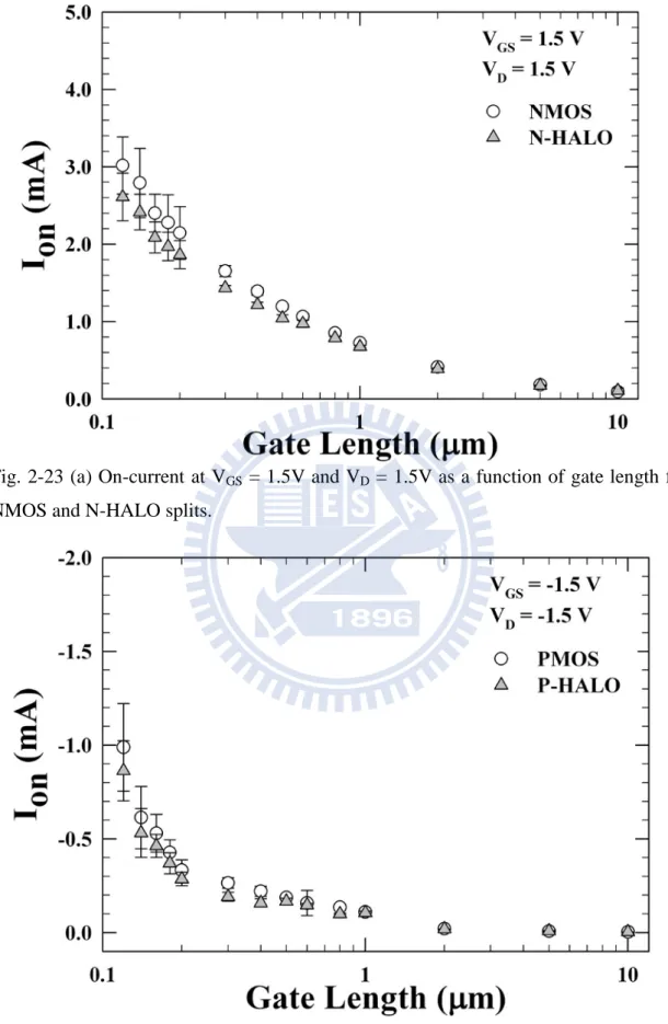
μm/120 nm. ………..………49 (b) Transfer characteristics of PMOS and P-HALO splits with W/L=10 μm/120 nm………..………..…49 Fig. 2-20 (a) Output characteristics of NMOS and N-HALO splits with W/L=10 μm/120 nm. ……….……...50 (b) Output characteristics of PMOS and P-HALO splits with W/L=10 μm/120 nm………..…….……...50 Fig. 2-21 (a) Threshold voltage as a function of gate length for NMOS and N-HALO splits. ………51 (b) Threshold voltage as a function of gate length for PMOS and P-HALO splits ……….……51 Fig. 2-22 (a) Drain induced barrier lowering (DIBL) as a function of gate length for
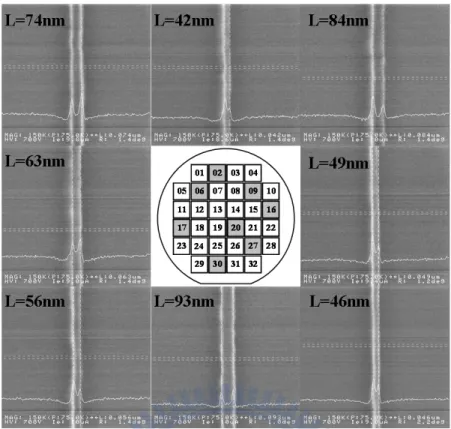
NMOS and N-HALO splits. ………52 (b) Drain induced barrier lowering (DIBL) as a function of gate length for PMOS and P-HALO splits………...…………52 Fig. 2-23 (a) On-current at VGS = 1.5V and VD = 1.5V as a function of gate length for
NMOS and N-HALO splits. ………....53 (b) On-current at VGS = -1.5V and VD = -1.5V as a function of gate length for
PMOS and P-HALO splits………...……....53
Chapter 3
Fig. 3-1 Lithography roadmap for DRAM, MPU and Flash [1]. ………...68 Fig. 3-2 (a) Mask layouts for defining the gate pattern and observed area on the active
region. A single mask is used in the single-patterning process. ………..……..69 (b) Mask layouts for defining the gate pattern and observed area on the active region. Gates 1 and 2 represent the two masks used in the DP process.……..90 Fig. 3-3 In-line SEM images patterned by the shaped-beam
tool. ………..………70 Fig. 3-4 In-line SEM images patterned by the Gaussian-beam tool. ………..…70 Fig. 3-5 In-line SEM images patterned by the PR ashing method after over-ashing process. ………..……..71 Fig. 3-6 In-line SEM images patterned by the PR ashing method. …………...71 Fig. 3-7 In-line SEM images patterned by the DP
method. ………...……….72 Fig. 3-8 Major process steps for fabricating n-MOSFETs with the Modified I-DP
method. (a) Deposition of TEOS oxide hard mask and in situ phosphorus-doped poly-Si layers onto the HfO2 gate dielectric (active region)
with LOCOSisolation. (b) Generation of first PR pattern (G1), followed by the anisotropic etching of hard mask layer. (c) Lateral etching of the hard mask layer, followed by the PR removal and the first anisotropic etching of poly-Si layer. (d) Generation of second PR pattern (G2). (e) Completion of the poly-Si gate pattern after second hard mask and poly-Si etching, and subsequent PR removal. (f) Formation of S/D junctions. ………..…..72
Fig. 3-9 In-line SEM images patterned by the Modified I-DP
method. ………..73
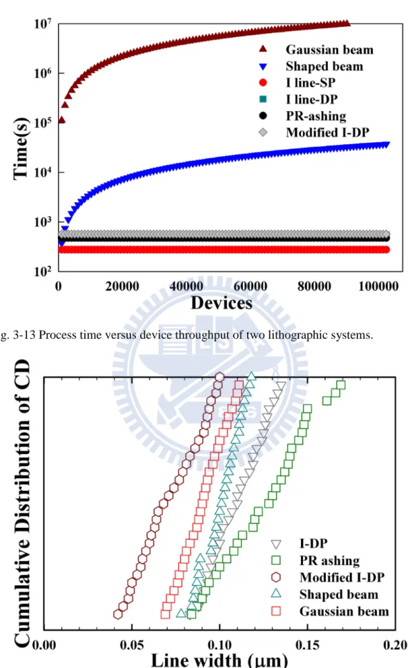
Fig. 3-10 In-line SEM images of dense line patterns generated by the Modified I-DP method compared with single patterning method (I-SP). ………..73 Fig. 3-11 Cross-sectional TEM image of a fabricated nMOSFET………..74 Fig. 3-12 Throughput of two lithographic systems. ………....74 Fig. 3-13 Process time versus device throughput of two lithographic
systems. ………75
Fig. 3-14 CD distribution of two lithographic systems. ………75
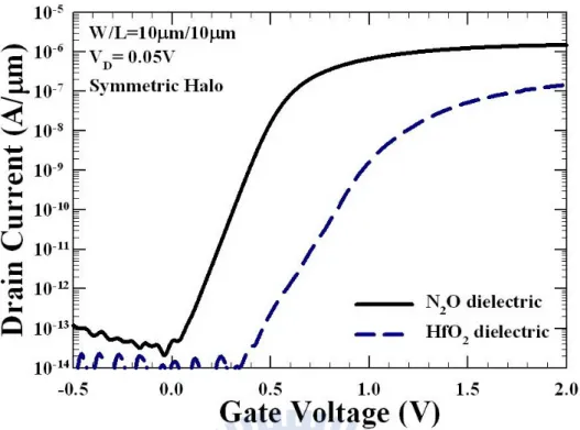
Fig. 3-15 (a) Transfer characteristics of two gate dielectric splits measured at VD =
0.05V with gate length of 10 μm and gate width of 10 μm. ……….………..76 (b) Output characteristics of two gate dielectric splits with gate length of 10 μm and gate width of 10 μmmeasured at VGS-Vth = 0 ~ 2 V, step= 0.4 V, and
VD = 0 ~ 2 V……….…………..…..76
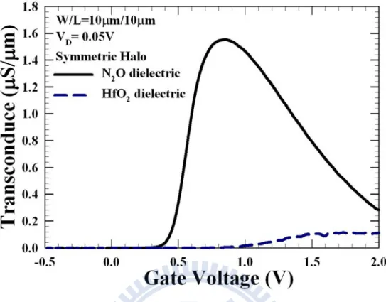
Fig. 3-16 Transconductance curves of two gate dielectric splits measured at VD = 0.05V
with gate length of 10 μm and gate width of 10 μm. ………...………...77 Fig. 3-17 Transfer characteristics of two gate dielectric splits measured at VD = 0.05 and
2 V with gate length of 45 nm and gate width of 10 μm. ………...77 Fig. 3-18 (a) Transfer characteristics of Symmetric and Asymmetric Halo splits
measured at VD = 0.05 and 2 V with gate length of 45 nm and gate width of 10
μm. ………...78 (b) Output characteristics of Symmetric and Asymmetric Halo splits with gate length of 45 nm and gate width of 10 μmmeasured at VGS-Vth = 0 ~ 2 V, step=
0.4V, and VD=0~2
V………...78 Fig. 3-19 (a) Transfer characteristics of Symmetric Halo split with HfO2 dielectric
measured at VD= 0.05 V with W/L = 50 μm/50 μm. ………..79
(b) Transfer characteristics of Symmetric Halo split with HfO2 dielectric
measured at VD = 0.05 V with W/L = 20 μm/20 μm………..………..79
(c) Transfer characteristics of Symmetric Halo split with HfO2 dielectric
measured at VD= 0.05 V with W/L = 10 μm/10 μm………..………..80
Fig. 3-20 Capacitance-Voltage (C-V) characteristics of HfO2 dielectric split randomly
sampled at eleven different dies of a six-inch wafer with gate length of 5 μm and gate width of 10 μm. The measurement frequency is 100 kHz. ………...80 Fig. 3-21 Threshold voltage as a function of gate length for Symmetric and Asymmetric Halo splits………...81 Fig. 3-22 Current drivability (Ion) as a function of gate length for Symmetric and
Asymmetric Halo splitsmeasured at VGS-Vth = 2 V and VD = 2 V. ...81
Chapter 4
Fig. 4-1 Schematic diagram of a TFET. ………..………...107
Fig. 4-2 Energy band diagrams of a TFET operated in the on/off-states……….107 Fig. 4-3 Major process steps for fabricating TFETs with the DP method. (a) Formation
of gate oxide and poly-Si on Si wafer with LOCOS isolation. (b) Generation of first PR pattern (G1), (c) First poly-Si etching and drain-junction implant. (d) Generation of second PR pattern (G2), (e) Second poly-Si etching and source-junction implant. (f) Completion of poly-Si gate after second PR removal………...108 Fig. 4-4 Major process steps for fabricating nMOSFETs with the DP method. (a)
Deposition of TEOS oxide hard mask and in situ phosphorus-doped poly-Si layers onto N2O gate dielectric (active region) with LOCOS isolation. (b)
Generation of first PR pattern (G1), (c) First oxide/poly-Si etching. (d) Generation of second PR pattern (G2), (e) Second poly-Si etching. (f) Completion of poly-Si gate after second PR removal, and formation of spacer, halo and S/D junctions………108
Fig. 4-5 Cross-sectional SEM image of a fabricated nMOSFET with nominal gate length of 80 nm………...…109 Fig. 4-6 Cross-sectional views of TFETs and the four splits of nMOSFETs……...…109 Fig. 4-7 Schematic illustrations for the charge pumping measurements with (a) fixed
peak sweep, (b) fixed base sweep, and (c) fixed amplitude sweep……...….110 Fig. 4-8 Basic setup for charge pumping measurements……….…..…...110 Fig. 4-9 Measurement setup for single-junction charge pumping measurement.…...111 Fig. 4-10 Schematic setup for flicker noise measurements………..……..111 Fig. 4-11 Transfer curves of TFETs for different source dose splits with W/ L = 10
μm/0.2 μm………..……..……...112 Fig. 4-12 Absolute value of source current versus source voltage curves with various
channel length (0.2/0.5/1μm) and W of 10 μm. The gate is floating during measurements………..……..…….112 Fig. 4-13 Absolute value of source current versus source voltage curves with various
channel length (50/60/80/100nm) and W of 10 μm. The gate is floating during measurements………..…………..…….113 Fig. 4-14 Length dependence of transfer characteristics for nMOSFETs with various
channel length and W = 10 µm biased at VD =1.2 V and VS =0 V. …..…….113
Fig. 4-15 Length dependence of transfer characteristics for TFETs with various channel length and W = 10 µm biased at VD =0.5 V and VS = -0.5 V……….114
Fig. 4-16 Transfer characteristics of a TFET with constant VDS (1.25V) but different S/D
biases. W/L = 10 µm/0.2 µm………..114 Fig. 4-17 The simulated doping concentration of boron in the source junction for the
fabricated TFETs………..………..115 Fig. 4-18 Transfer characteristics of all splits measured at VD=0.05 and 1.2 V with W/L
= 10 μm/80 nm………..………...………..115 Fig. 4-19 Transconductance characteristics of all splits measured at VD=0.05 V with
W/L = 10 μm/80 nm………..………...………..116 Fig. 4-20 Output characteristics of all splits measured at VG -Vth = 0~2 V and step = 0.4
V with W/L = 10 μm/80 nm. ………..………..……...………..116 Fig. 4-21 Threshold voltage roll-off characteristics of all splits measured at VD = 0.05 V
with W/L = 10 μm/80 nm………..………..……...………..……..117 Fig. 4-22 DIBL as a function of channel length for all splits measured at VD = 0.05 V
with W = 10 μm…………..………..……...………..……….117 Fig. 4-23 Substreshold swing as a function of channel length for all splits measured at
VD= 0.05 V with W = 10 μm……..……...………..……….….118
Fig. 4-24 On-current as a function of channel length for all splits measured at VG -Vth =
1 V and VD= 1.2 V with W = 10 μm. ……...………..………..118
Fig. 4-25 Off-current as a function of channel length for all splits measured at VG = 0 V
and VD= 1.2 V with W = 10 μm…...………...………..119
Fig. 4-26 Transfer characteristics of 15 Control nMOSFETs, with W/L = 10 μm/80 nm measured at VD = 1.5 V…...………...………....119
Fig. 4-27 Transfer characteristics of 15 Sym-Halo nMOSFETs, with W/L = 10 μm/80 nm measured at VD = 1.5 V………...……….………....120
Fig. 4-28 Transfer characteristics of 15 Asy-Halo nMOSFETs, with W/L = 10 μm/80 nm measured at VD = 1.5 V...………...………...120
Fig. 4-29 Transfer characteristics of 15 Asy-Halo-R nMOSFETs, with W/L = 10 μm/80 nm measured at VD = 1.5 V. ………...……….………...121
Fig. 4-30 Substrate current (Isub) versus gate voltage for all splits of devices measured at
VDof 3 V with W/L = 10 μm /100 nm. ………...……….……….121
Fig. 4-31 Impact ionization rate (Isub/ID) for all splits of devices measured at VD of 3 V
with W/L = 10 μm /100 nm……...……….………....122 Fig. 4-32 Subthreshold characteristics and transconductance of Control device before
and after 5000-second of hot-electron stressing measured at VD of 0.05 V with
W/L = 10 μm /100 nm……...……….………....122 Fig. 4-33 Subthreshold characteristics and transconductance of Sym-Halo device before
and after 5000-second of hot-electron stressing measured at VD of 0.05 V with
W/L = 10 μm /100 nm...……….………....123 Fig. 4-34 Subthreshold characteristics and transconductance of Asy-Halo device before
and after 5000-second of hot-electron stressing measured at VD of 0.05 V with
W/L = 10 μm /100 nm……….………...…....123 Fig. 4-35 Subthreshold characteristics and transconductance of Asy-Halo-R device
before and after 5000-second of hot-electron stressing measured at VD of 0.05
V with W/L = 10 μm /100 nm…….………...124 Fig. 4-36 Threshold voltage shift as a function of stress time for all splits of devices
measured at VD of 0.05 V with W/L = 10 μm /100 nm. The hot-electron
stressing was performed at VD = 3 V and VG at maximum substrate
current...124 Fig. 4-37 Transconductance degradation as a function of stress time for all splits of
devices measured at VD of 0.05 V with W/L = 10 μm /100 nm. The
hot-electron stressing was performed at VD = 3 V and VG at maximum
substrate current...125 Fig. 4-38 The increase in interface state density as a function of stress time for all splits of devices measured at VD of 0.05 V with W/L = 10 μm /100 nm. The
hot-electron stressing was performed at VD = 3 V and VG at maximum
substrate current...125 Fig. 4-39 The increase in charge pumping current after 5000-second of hot carrier stress for all splits of devices with W/L = 10 μm /100 nm. The hot-electron stressing was performed at VD = 3 V and VG at maximum substrate current...126
Fig. 4-40 Non-uniform distribution of local threshold voltage and flat-band voltage across the device caused by variation of lateral doping concentration. (x=0 is at the drain junction and direct to source junction) ...126 Fig. 4-41 Derivation of the relationship between local threshold voltage and lateral
distance x from the single-junction charge pumping data of the control device………..127 Fig. 4-42 Extracted lateral profile of local threshold voltage near the graded drain
junction in the control sample………....127 Fig. 4-43 Charge pumping current before and after 5000-second of hot-electron stressing
(VG@Isubmax and VD= 3 V) with W/L = 10 μm /100 nm………...128
5000-second of hot-electron stressing (VG@Isubmax and VD = 3 V) with W/L =
10 μm /100 nm………...128 Fig. 4-45 Drain current noise spectrum density (Sid) of a virgin Control device measured
at gate overdrive of 0.1 V (VG –Vth = 0.1 V) and VD = 0.05 V with W/L = 10
μm/100 nm…………...129 Fig. 4-46 Drain current noise spectrum density for all splits of virgin devices measured
at a gate overdrive of 0.1 V (VG –Vth = 0.1 V) and VD = 0.05 V with W/L = 10
μm/100 nm………...129 Fig. 4-47 Normalized noise power spectrum density (Sid/ID2) and (gm/ID)2 as a function
of drain current for Control device with W/L = 10 μm/0.2 μm at 100 Hz. ...130 Fig. 4-48 Normalized noise power spectrum density (Sid/ID2) and (gm/ID)2 as a function
of drain current for Sym-Halo device with W/L = 10 μm/0.2 μm at 100 Hz. ……….130 Fig. 4-49 Normalized noise power spectrum density (Sid/ID2) versus gate overdrive
(VG–Vth) for all splits of devices with W/L = 10 μm/10 μm at 100 Hz…….131
Fig. 4-50 Normalized noise power spectrum density (Sid/ID2) versus gate overdrive
(VG–Vth) for all splits of devices with W/L = 10 μm/0.1 μm at 100 Hz. .….131
Fig. 4-51 Drain current noise spectrum density for all splits of stressed devices measured at gate overdrive of 0.1 V (VG –Vth = 0.1 V) and VD = 0.05 V with W/L = 10
μm/100 nm………..132 Fig. 4-52 Normalized noise power spectrum density (Sid/ID2) versus gate overdrive
(VG–Vth) before and after 5000-second of hot-electron stressing for Control
device with W/L = 10 μm/0.1 μm at 100 Hz. ………132 Fig. 4-53 Normalized noise power spectrum density (Sid/ID2) versus gate overdrive
(VG–Vth) before and after 5000-second of hot-electron stressing for Sym-Halo
device with W/L = 10 μm/0.1 μm at 100 Hz. ………133 Fig. 4-54 Normalized noise power spectrum density (Sid/ID2) versus gate overdrive
(VG–Vth) before and after 5000-second of hot-electron stressing for Asy-Halo
device with W/L = 10 μm/0.1 μm at 100 Hz………..133 Fig. 4-55 Normalized noise power spectrum density (Sid/ID2) versus gate overdrive
(VG–Vth) before and after 5000-second of hot-electron stressing for
Asy-Halo-R device with W/L = 10 μm/0.1 μm at 100 Hz………...…..134 Fig. 4-56 The increase in normalized noise power spectrum density (ΔSid/ID2) versus
gate overdrive (VG–Vth) after 5000-second of hot-electron stressing for all
splits of devices with W/L = 10 μm/0.1 μm at 100 Hz. …………...………..134
Chapter 5
Fig. 5-1 Key fabrication process flow of the proposed GAA JL NWFET. (a) Deposition and patterning of a sandwich stack of nitride/TEOS oxide/nitride layers on Si substrate capped with 200-nm-thick wet oxide, followed by selective lateral etching of TEOS oxide layer using DHF to form sub-100-nm cavity underneath both sides of the top nitride. (b) Deposition of an in situ phosphorus-doped poly-Si layer. (c) Simultaneous definition of NW doped channels and S/D regions. (d) Etching of the nitride and oxide, followed by the ALD deposition of the high-κ/metal gate stack structure (10-nm Al2O3 and
10-nm TiN). (e) Sputter deposition of another 140 nm TiN film to make a final gate electrode of 150 nm. (f) Schematic top-view layout of the
device.. ………..……….164
Fig. 5-2 Tilted scanning electron microscopic (SEM) images before and after cavity formation. ………...……….165 Fig. 5-3 Tilted SEM images of different-sized NW devices before the gate stack
formation. (a) A tiny NW device showing NWs exposed on both sides of the temporary dielectric step, (b) a mid-sized NW device, and (c) a large-sized NW device………..………..…….165 Fig. 5-4 Cross-sectional HRTEM image of a fabricated GAA JL NWFET with the
TEOS oxide/TiN gate stack. A NW size is around of 12 nm in thickness (T) and 23 nm in width (W). The inset is the corresponding diffraction pattern of the NW, revealing the monocrystalline structure of the grain with [110] orientation. ………..………..……….165 Fig. 5-5 TEM and tilted SEM images of fabricated JL devices. (a) Cross-sectional TEM image of a JL device with tiny NW covered with Al2O3/TiN GAA stack. 52°
tilted SEM images of a mid-sized JL device with a NW cross section of 75 × 30 nm and a large-sized JL device with a NW cross section of 152 × 74 nm. ……….166 Fig. 5-6 Key fabrication process flow of the proposed GAA JL NW SONOS memory
device. (a) Deposition and patterning of a sandwich stack of nitride/TEOS oxide/nitride layers on Si substrate capped with 200-nm-thick wet oxide. (b) Selective lateral etching of TEOS oxide using DHF to form a sub-100-nm cavity underneath both sides of the top nitride. (c) Deposition of an in situ phosphorus-doped poly-Si layer. (d) Simultaneous definition of the NW doped channels and S/D regions, followed by etching off the nitride and oxide surrounding the NW channels. (e) LPCVD deposition of gate dielectric stack of blocking oxide/trapping nitride/tunneling oxide (ONO) with thicknesses of 12/7/3 nm. (f) Deposition and patterning of an in situ phosphorous doped n+-poly-Si layer as the gate electrode. ……….……….167 Fig. 5-7 Schematic illustrations of gate structures (GAA/Ω-gate) implemented in our
JL-SONOS memory cells. ……….………...168 Fig. 5-8 (a) Top-view SEM and cross-sectional TEM images of the NW channel with
(b) GAA and (c) Ω-gate
structures. ……….………..………...168 Fig. 5-9 Illustration of the key steps for building 3-D multilayer stacked JL poly-Si NW
device. (a) Formation of sub-100 nm cavities. (b) Formation of channel and S/D. ……….………..……….169 Fig. 5-10 Tilted SEM images of anisotropically-etched dummy patterns. …...……….169 Fig. 5-11 Overhead-view SEM images of the nano-cavities with (a) 30- and (b)
40-second lateral-etching time. ………..………170 Fig. 5-12 Cross-sectional TEM images of fabricated 3-D stacked JL NW memory device. ………..………..………170 Fig. 5-13 Key fabrication process flow of the proposed planar JL poly-Si TFT. (a)
Growth of 1000-nm-thick oxide by wet oxidation on a six-in silicon substrate as the buried oxide. (b) Deposition of a 9-nm-thick in situ phosphorous doped n+-poly-Si layer as the channel layer. (c) Successive depositions of a 13-nm
TEOS oxide as the gate dielectric and a 200-nm in situ n+-poly-Si as the gate electrode, followed by the gate pattern definition. (d) Formation of sidewall spacers (20-nm TEOS oxide layer and 20-nm nitride layer). (e) Depositions of a 5-nm-thick nickel layer and a 15-nm-thick titanium nitride layer. (f) Annealing process for forming NiSi on the gate, and S/D regions. ………..171 Fig. 5-14 Top-view SEM and cross-sectional TEM images of the fabricated planar JL
poly-Si TFT. …………..………..………..172 Fig. 5-15 S-parameter measurement system. ………..………..172 Fig. 5-16 Equivalent circuit diagram used for the two-step correction including parasitic
effect. ………..………..……….173 Fig. 5-17 (a)The open test fixture and (b) the diagram of equivalent circuit. ……..….173 Fig. 5-18 (a)The short test fixture and (b) the diagram of equivalent circuit. …..…….174 Fig. 5-19 Transfer characteristics of JL and IM NWFETs with an NW channel dimension of W/T = 23 nm/12 nm and a channel length (L) of 1 μm measured at VD = 0.5 and 2 V. ………..……….174
Fig. 5-20 Comparison of transconductance versus gate voltage for the JL and IM devices
at VD = 0.5 V. ………..………..……….175
Fig. 5-21 Measured total resistance Rtotal ≡ VD/ID = RSD + Rch versus channel length
for JL and IM NWFETs measured at VG – Vth of 4 V and VD of 0.15 V. …..175
Fig. 5-22 Transfer characteristics of the JL and IM NW devices. Mid-sized (75 × 30 nm) and large-sized (152 × 74 nm) JL NW devices are also plotted for comparison. All devices characterized here are with channel length of 0.4 μm. ……….176 Fig. 5-23 Output characteristics of JL and IM splits measured at VG - Vth = 0 ~ 2 V and
step = 1 V with L = 0.4 μm. ………..……….176 Fig. 5-24 Transconductance (Gm) and increments of Gm as a function of gate length for
JL and IM splits measured at VD = 0.5 V. ……..………...…….177
Fig. 5-25 Threshold voltage (Vth) as a function of gate length for JL and IM splits
measured at VD = 0.5 V. ………..……….…..177
and IM splits extracted at VG - Vth = 2 V and VD = 0.5 V. ………....178
Fig. 5-27 Tilted SEM and cross-sectional TEM images of a fabricated GAA JL NWFET with L=5 μm showing collapse of NWs in the central channel region with an omega-shaped gate structure. The inset shows a NW device with L=1 μm depicting normal suspension of NWs between the S/D regions. …….…....178 Fig. 5-28 Programming properties of the JL and IM NW SONOS devices at gate biases
of 9, 11, and 13 V. ………..………..……..179 Fig. 5-29 Transfer characteristics of JL SONOS split in the programmed states biased at
VG = 13 V for various duration times. ……….……..179
Fig. 5-30 Multilevel programming behavior of the JL NW device. Transfer characteristics of JL SONOS device with gate biases of 9, 11, and 13 V for 100 ns. Inset shows the definition of Vth range for each state. …………...……..180
Fig. 5-31 Erasing properties of the JL and IM NW SONOS devices at gate biases of -9, -11, and -13 V. Before erasing, the cells were programmed to Vth shift of +3 V
and +2.5 V for the JL and IM structures, respectively. …………...…….…..180 Fig. 5-32 Retention behaviors for the JL and IM NW SONOS devices at room
temperature. ……...…….………...181 Fig. 5-33 Endurance behaviors for the JL and IM NW SONOS devices at room
temperature. …...…….………...181 Fig. 5-34 Transfer characteristics of GAA-L, Ω-L, GAA-H and Ω-H JL NW SONOS
devices measured at VD = 0.5 and 2 V. ………..182
Fig. 5-35 Programming behaviors for GAA-L, Ω-L, GAA-H and Ω-H JL NW SONOS devices. The programming gate bias is 11 V. ………182 Fig. 5-36 Erasing behaviors for GAA-L, Ω-L, GAA-H and Ω-H JL NW SONOS devices.
The Erasing gate bias is -11 V. ………..183 Fig. 5-37 Retention behaviors for the GAA-L and GAA-H JL NW SONOS devices at
room temperature. ……….183 Fig. 5-38 Retention behaviors for the Ω-L and GAA-L JL NW SONOS devices at room
temperature………184 Fig. 5-39 Transfer characteristics and the affiliated cross-sectional SEM image of a
non-working 3-D JL device. ……….……….184 Fig. 5-40 Cross-sectional SEM image of a non-working 3-D JL device. ……….185 Fig. 5-41 Transfer and output characteristics of both 1-level and 3-level JL splits with L
= 1 μm, (a) measured at VD = 0.1 and 2 V, (b) VG - Vth = 0 ~ 4 V with step = 2
V. ……….…...185 Fig. 5-42 Cumulative distribution of Vth for both 1-level and 3-level JL splits with L = 1
μm measured at VD = 0.1 V. ………...186
Fig. 5-43 Cumulative distribution of SS for both 1-level and 3-level JL splits with L = 1 μm measured at VD = 0.1 V. ………...186
Fig. 5-44 Cumulative distribution of Ion for both 1-level and 3-level JL splits with L = 1
μm extracted by maximum drain current at VD = 2 V. ………...187
Fig. 5-45 Cumulative distribution of Ioff for both 1-level and 3-level JL splits with L = 1
μm extracted by minimum drain current at VD = 2 V. ………...187
Fig. 5-46 Transfer characteristics of both JL and IM planar poly-Si TFTs with W/L = 8/0.4 μm measured at VD = 0.1 and 2 V. ……….………...188
Fig. 5-47 Output characteristics of both JL and IM planar poly-Si TFTs with W/L = 8/0.4 μm measured at VG - Vth = 0 ~ 3 V with step = 1 V. ………...188
Fig. 5-48 Drain-current noise power spectral density (Sid) versus frequency for both JL
and IM planar poly-Si TFTs with W/L = 8/0.4 μm measured at VGS - Vth =0.5
V and VD = 0.1 V. ………...…………...189
Fig. 5-49 (Symbols) Sid/Id2 and (dashed lines) (gm/Id)2 versus drain current for both JL
and IM planar poly-Si TFTs with W/L = 8/0.4 μm measured at VD = 0.1
V. ……….…………..189 Fig. 5-50 H21 and U of JL device measured at VD of 2 V and (VGS − Vth) of 4 V with
W/L = 8/0.4 μm. ……….….……..190 Fig. 5-51 H21 and U of IM device measured at VD of 2 V and (VGS − Vth) of 4 V with
W/L = 8/0.4 μm. ……….…….……..190 Fig. 5-52 ft and fmax of the JL and IM devices measured at VD of 2 V and (VGS− Vth) of
0.5–3.5 V with respect to the drain current. ……….………..191 Fig. 5-53 The cross section of the fabricated TFT with corresponding small-signal
equivalent circuit. ………..…….…….……..191 Fig. 5-54 The extraction results of extrinsic resistances. ………..…….……….……..192 Fig. 5-55 The extraction results of Im(Y11)+Im(Y12), -Im(Y12), and Im(Y12)+Im(Y22) as
a function of the angular frequency. ………..…….…….………..192 Fig. 5-56 The extraction results of gm and ro as a function of the angular frequency. ..193
Fig. 5-57 The extraction results of τ as a function of the angular frequency. ………...193 Fig. 5-58 The modeling results of the fabricated TFT (a) S11 and S22 and (b) S12 and S21
Chapter 1
Introduction
1.1 General Background
1.1-1 Double Patterning Technique
The well-known Moore’s Law describes that the number of transistors on an integrated circuit (IC) chip will double every 18 months [1-2]. Since the advent of IC manufacturing, this law has been in force for decades. In order to keep up with the Moore’s Law, shrinkage in device dimensions is indispensable, which also promotes device density, operation speed, and chip functionality. In other words, for better performance and cheaper manufacturing cost, the continuous scaling of the devices is evitable. To keep pace with the law, it requires innovation to overcome several fundamental physical barriers lying ahead, and first of all is to extend the photolithography limit. According to the Rayleigh’s criterion, the resolution, R, of a photolithography technique can be expressed as follows [3]:
NA
k
R= 1λ (1-1), where k1 is a system constant, λ is the wavelength of incident light, and NA is the numerical aperture of the lithography system. Based on such criterion, we could adjust the three factors of the criterion so as to boost the resolution of a lithography system [4-6]. Recently, it was reported that the double exposure (DE) technique [7], and double patterning (DP) technique [8-10] were being considered as the promising candidates to extend lithography processing beyond the 45 nm node at k1 factors below 0.30. DP is a process that splits one patterning step into two to relax the imaging fidelity requirements for small technology nodes. The most common form of DP typically decomposes a target layout pattern into two separate photomasks employing two exposure steps and subsequent etching steps. Consequently, the dimensions of the final target patterns can easily break the resolution limit with single exposure. Usually I-line stepper is not capable of sub-100 nm pattern generation owing to its long exposure wavelength of 365 nm. In this work, we develop a DP technique with conventional I-line stepper to generate sub-100 nm photoresist (PR) patterns with the goal to fabricate nano-scale
MOSFETs. Although this technique consists of two times the lithographic and subsequent etching steps, we show that the DP method could reliably generate line patterns with dimension down below 100 nm.
1.1-2 Junctionless Technique
For the sake of keeping pace with the Moore’s Law, continuously downscaling the dimension of the semiconductor devices is indispensable to maintain device functionality and make manufacturing cost cheaper. However, the traditional planar bulk MOSFET structure used in the past decades inherently consists of two PN junctions, the source/drain-to-channel junctions, and the extremely high doping concentration gradient of S/D region causes the fluctuation of diffusing impurities especially within a range of few nanometers for the nano-scale devices [11]. To precisely control the doping prolife of S/D region, it needs an excessively tight and efficient thermal process for the dopant activation, which imposes more challenges on the device fabrication with the continuous shrinkage of device dimension.
To address the aforementioned challenge of controlling the doping profile, a novel device named “junctionless (JL) field-effect transistor” has been revived recently [12-14], while the same idea has been revealed in an old patent filed by Lilienfeld in 1926 [15]. In a JL transistor, the same doping polarity and concentration are used throughout the entire device from the source, channel to drain. Furthermore, the operation of a JL transistor is different from that of an accumulation-mode device, and is inherently a gated resistor in the on-state. In particular, a JL transistor is turned off through full depletion of carriers in the channel by the gate in the off-state. Besides, the much higher doping concentration in the channel, larger than 1019 cm-3, is the unique feature of JL transistor, and is different from an accumulation-mode transistor. Due to the inherently homogeneous doping concentration across S/D and channel in the JL transistor, no conventional p-n junctions are present in it. Therefore, the JL technique can relieve the constraints related to the formation of the ultra-shallow or ultra-abrupt junction encountered in the conventional inversion-mode (IM) transistor, thus the fabrication process can be greatly simplified and the manufacturing cost can be cheaper as well.
With the dimensional scaling of the MOSFETs, it accompanies a lot of challenges including the increasingly rising off-state leakage current and the short channel effects (SCE), such as the threshold voltage (Vth) roll-off, the drain induced barrier lowering
(DIBL), and bulk punch-through. As for the IC industry, which has traditionally been driven by the Moore’s Law, it has brought about catastrophic power consumption, and thus the emergent demand for lower power supply is without any description. But it also requires a coexisting reduction in the threshold voltage to sustain the device performance leveraging the Moore’s Law. Nevertheless, a concomitant increase in off-state leakage is inevitable due to the restriction of non-scalable subthreshold swing (SS). For the sake of leakage current reduction, low power consumption and good SCE immunity, optimization of the source and drain junctions separately would be an effective scheme.
The asymmetric MOSFET with asymmetric lightly-doped drain (LDD) architecture [16-17] was fabricated by using additional implantation mask, followed by formation of selective oxide deposition. However, the latent misalignment would obstruct the device scaling. Fortunately, the self-aligned asymmetric structure [18] was proposed to settle the aforementioned issue. But, unfortunately, the inevitable use of phosphoric acid would likely be another issue resulted from the gate oxide damage caused by isotropic etching of phosphoric acid. The implantation scheme is an approach to achieve an asymmetric architecture as well. As described in [19], the implementation of tilt-angle implantation facilitated the fabrication of asymmetric architecture. Nonetheless, the shielding of denser gate electrodes would increase more challenges in the adoption of tilt-angle implantation with downscaling. On the other hand, the halo doping scheme employed in standard CMOS process certainly can be adopted to accomplish the asymmetric structure in terms of boosting the device performance as reported in [20-22]. The adoption of source-junction-only halo doping scheme can not only reduce the capacitance of n+p junction at the drain junction but also the electrical field of drain side. Therefore the issue of leakage current can effectively be relieved, and further the power consumption can be reduced.
With the ever-increasing concerns about the forthcoming exhaust of petroleum in the near future and the unavoidable power consumption by the IC appliances, the green technology is highly demanded for reducing the supply voltage of CMOS logic devices. The most fundamental limitation that controls the turn-on efficiency of a transistor stems from its inherent properties related to thermodynamic carrier distribution. The
basic drift-diffusion theory gives the physical limitation on the subthreshold swing (SS) at 60 mV/dec at room temperature [23]. The concept of tunneling field-effect transistor (TFET) was proposed by Sanjay Banerjee et al. in 1987 [24] and called “surface tunneling transistor” as well in those days [24-26]. The TFET is inherently a gated p-i-n diode and certainly can be categorized as an asymmetric S/D device as depicted in Fig. 1.1, using band-to-band tunneling (BTBT) as carrier transport mechanism. As a result, TFETs do not undergo the same physical limitation as MOSFETs, and are a promising candidate for achieving sub-60 mV/dec of SS.
1.1-4 Flicker Noise Characteristics
In an electronic circuit, currents and voltages are randomly perturbed from their given values because of inextricable interference of noise. Considering the random nature of noise, it can’t be excluded thoroughly and further restricts the accuracy of measured results eventually [27-28]. Hence, in view of both science and engineering, noise is a basic problem, essential to comprehend and consider for the sake of alleviating its effects and increasing the precision of desired signals. There are many kinds of noise sources such as thermal noise, shot noise, generation-recombination (g-r) noise, random-telegraph-signal (RTS) noise, and flicker (1/f) noise [29-35]. Because the transistor dimensions have been continuously downscaled, CMOS technology has been developed for the RF and analog applications which were governed by bipolar transistors in the past [36-40]. For low-noise RF/analog applications, low 1/f noise in MOSFETs is an important requirement. Therefore, accurate MOSFET noise models are highly correlated with circuit designers as well as semiconductor manufacturers that are required to pay attention to reducing the 1/f noise in transistors.
The flicker noise in MOSFETs has been extensively studied for more than two decades [41-47]. The flicker noise, called 1/f noise as well, is the common name for the fluctuations with its power spectral density proportional to 1/fγ, with γ close to 1, usually in the range of 0.7 to 1.3. In the past, there were two major theories to explain the physical origins of flicker noise in MOSFETs. One is the number fluctuation theory based on McWhorter’s charge trapping model [43]. The other is the bulk mobility fluctuation theory based on Hooge’s empirical relation [48].
In the carrier number fluctuation theory, the random trapping and detrapping processes of charges occurred in the oxide traps near the interface between Si channel
and SiO2 are the culprit of flicker noise [41-42], [49-50] which was originally presented
by McWhorter in 1957 [43]. The charge fluctuation influences fluctuation of the surface potential, and further the channel carrier density is modulated. The conventional number fluctuation theory predicts that the 1/f noise power in the linear region is given by
2 2 ( ) ( ) d t fn eff Id N E I S f fWLN γ = (1-2),
where Nt(Efn)eff is the effective oxide trap density at the quasi Feimi level; Id is the drain current; f is frequency; N is the number of channel carrier per unit area; γ is the attenuation coefficient of electron wave function in the oxide and the value is typically taken to be 108 cm-1 for the Si-SiO2 system [51]; W and L are channel width and length,
respectively.
On the other hand, the mobility fluctuation theory considers 1/f noise as a result of fluctuation in bulk mobility, and moreover, the spectral density in a homogeneous material based on Hooge’s empirical relation can be given by
2 ( ) d H Id I S f fWLN α = (1-3), where SId is the spectral density of the noise in the current; Id is the drain current; f is the frequency; N is the number of channel carriers per unit area; αH is the Hooge’s parameter with a value of around 2 × 10⁻³ [46]; W and L are channel width and length, respectively.
Later a unified flicker noise model which was proposed by K. K. Hung [52] incorporated both the carrier number fluctuation theory and the mobility fluctuation mechanism to explain the origin of low-frequency noise in a correlated manner. The total drain current noise power can be expressed as
2 2 2 0 2 0 1 1 ( ) ( , ) ( ) ( ) L L d Id Id t fn kTI S f S x f xdx N E dx L ∆ γ fWL N x αµ = ∆ = ±
∫
∫
(1-4),where Nt(Efn) is the oxide trap density at Fermi level Efn; N(x) is the number of channel carriers per unit area; α is the Columbic scattering parameter; γ is the attenuation coefficient and typically equals to 108 cm-1 [51]; The sign of the mobility term can be determined by fitting the expression with the measured data. For the majority of samples, the sign has to be chosen as positive. This equation is the basic expression of the unified flicker noise model. Furthermore, we can yield the input referred noise power by virtue of dividing SId by the square of the transconductance, and the formula
can be given by 2 2 2 2 ( ) ( ) Id (1 ) ( ) Vg t fn m ox S f kTq S f N N E g γ fWLC αµ = = + (1-5).
1.1-5 Radio Frequency Techniques
In the past, wireless communication industry was regarded as an important part of the defense industry due to the importance of instantaneous transmission, and its mysterious muffler was gradually taken off until Cold War came to the end. People were looking forward to breaking the space constraint by virtue of wireless communication, and therefore the private enterprise found their motivation in the development of wireless communication industry nonstop. Based on the continuous development of the integrated circuit technology and the desperate demand for the people's livelihood application, it makes possible to bring out the cheap wireless communication products. However, human beings really manifest their hungers for larger capacity of data transmission after both the convenience and timeliness of the wireless transmission are met. In the case of no longer extra bandwidth being squeezed out through both the network protocol and the developments of systematic architecture, it is the fundamental solution to obtain a large number of bandwidth by increasing the communication frequency. While using the wireless communication technology for facilitating some innovative applications such as distant and timely medical care [53], immediate disaster warning, logistics management to create better living is another important target worthy of development. Therefore, how to attain low power operation and energy-saving goals is the common objective of relative research topic. Nonetheless, the core value of wireless communication development is the high-frequency technology regardless of oncoming developments of both wireless communication technology and application.
There are various high-frequency devices including heterojunction bipolar transistor (HBT) such as AlGaAs/GaAs HBT, InGaP/GaAs HBT and InP HBT of III-V compound semiconductors [54], or silicon based devices such as SiGe HBT and CMOS [55]. For the past decades, transistors have been widely used and continuously developed because the raw material of silicon is easily obtained and the correlated fabrication process is well mature. Moreover, IC manufacturing vendors have made great efforts to scale down the device’s gate length for achieving higher operation frequency of the circuits and further encroaching in the field of high-frequency
applications in recent years. There are various RF transmission chips constructed by transistors including voltage-controlled oscillator (VCO) [56], low-noise amplifier (LNA) [57], filter, mixer, and phase-locked loop (PLL) [58]. On the other hand, the RF performance of thin-film transistors (TFTs) is expected to improve significantly by properly shrinking the dimensions of devices, and further it is demonstrated that the polycrystalline silicon TFT technology is feasible for low-cost RF IC applications such as RF identification (RFID) and RF modules integrated on display panel [59-60].
1.2 Motivation
To keep pace with the Moore’s Law, it requires innovation to accomplish shrinkage in device dimensions, and first of all extending the photolithography limit is indispensable. 32 nm technology node mass production of nano-scale ICs employs the immersion lithography tools with the excimer laser to generate the nano-scale patterns [61]. However, the extremely high-cost equipment employed for high-volume manufacturing is not affordable in the university-based laboratories. Therefore, a large part of researches focused on the device size of nano-scale regime accomplished in the university-based laboratories barely count on some substitute methods, such as electron beam direct writing [62], ion beam lithography system [63], nanoimprint lithography [64], etc. In this dissertation, a simple method which combines both I-line lithographic process and double patterning (DP) technique, as stated in Sec.1.1-2, is proposed and developed to generate sub-100 nm photoresist (PR) patterns with the goal to fabricate nano-scale MOSFETs. In addition, the proposed lithographic technique was implemented to fabricate symmetric or asymmetric devices as stated in Sec. 1.1-4. The additional merit associated with the proposed DP process is increasing the flexibility in device design in terms of accomplishment of independent S/D engineering to promote the device performance.
On the other hand, polycrystalline silicon (poly-Si) thin-film transistor (TFT) technology has been very attractive for the flexible electronics, the emerging 3-D IC and system-on-panel (SoP) electronics integration owing to its low thermal budget and very mature fabrication processes [65-66]. In recent years, the nanowire (NW) TFTs with the implementation of NWs as the channels have been demonstrated with excellent device performance thanks to their inherently tiny volume and the following reduction of defects [67-68]. Furthermore, the NW TFT combined with multiple-gated (MG)
structure [69] benefits not only current drive, but also subthreshold slope, as well as better immunity to the short-channel effects thanks to better gate controllability for effectively controlling the electrostatic potential in its tiny NW channel. To cope with the issue of formation of extremely abrupt junctions, as mentioned in Sec. 1.1-3, NWTFT technology previously developed by our group with the MG configuration was adopted to implement the JL scheme by using one in situ doped poly-Si layer to serve as source, channel and drain junctions [70]. In this dissertation, we exploit the feasibility of JL technology through the fabrication and characterization of both MG NWTFT and planar ultrathin-channel TFT schemes, and furthermore adopt these JL devices in the applications of logic circuits, nonvolatile memory devices and even high-frequency techniques.
Owing to well developed and very mature fabrication processes of TFTs, the performance of TFTs has been greatly boosted to serve as not only the mainstream technology, the switches of pixels in the AMLCDs [71] at the start, but also the basic building blocks of ICs on the periphery of displays, SoP especially. In addition, with the thriving in portable electronics, wireless transmission among electronics equipment doubtlessly prevails throughout our daily life as mentioned in Sec. 1.1-6. However, owing to the relatively low mobility of poly-Si as compared with the bulk Si counterparts, as well as the quite giant device size in state-of-the-art manufacturing (e.g., channel length > 3 μm), few works are reported on studying the high-frequency characteristics of poly-Si TFTs. Therefore, in this dissertation, we undertook the studies to investigate the high-frequency characteristics of short-channel poly-Si TFTs (e.g., channel length < 3 μm), including the fabrication and characterization of both IM and JL planar poly-Si TFTs to demonstrate the feasibility of low-cost RF IC applications, as well as the related small-signal modeling and parameter extraction of fabricated devices.
1.3 Thesis Organization
Total seven chapters are contained in this dissertation.
In Chapter 1, the related backgrounds and motivations of this dissertation are described.
In Chapter 2, we have developed a simple method adopting double-patterning (DP) technique to extend the I-line stepper limit to define nano-scale structures. Through in-line and cross-sectional scanning electron microscopy analyses of the generated
patterns, we confirmed the feasibility of the DP technique for the fabrication of nano-scale devices. Resolution capability of this technique has been confirmed to be at least 100 nm, which is much superior to the resolution limit of conventional I-line lithography. Moreover, an unexpected obstacle, the etching issue of second gate pattern, occurred in the DP process is addressed as well.
In Chapter 3, we have developed a modified DP technique with an I-line stepper and also compared several lithographic techniques implemented as promising candidates for the purpose of patterning nano-scale structures in the university-based laboratories. By virtue of in-line and cross-sectional scanning electron microscopy analyses of the generated patterns, we confirmed the feasibility of the ameliorative DP technique for generating sub-30 nm line patterns, and furthermore some features of these lithographic techniques were discussed in terms of throughput, line edge roughness (LER), critical dimension uniformity (CDU), minimum line width, etc.
In Chapter 4, we have fabricated asymmetric devices, including asymmetric halo nMOSFETs and tunneling field-effect transistors (TFETs) after demonstrating the feasibility of DP technique in Chapter 2. In addition, several device performances of symmetric and asymmetric devices are discussed in terms of both dc characteristics and reliability tests such as hot-carrier stress and flicker noise characteristics.
In Chapter 5, we have investigated the feasibility of gate-all-around (GAA) polycrystalline silicon (poly-Si) nanowire transistors with junctionless (JL) configuration by utilizing only one heavily doped poly-Si layer to serve as source, channel, and drain regions. In situ n+-doped poly-Si material features high and uniform-doping concentration, facilitating the fabrication process and reducing the process cost. Moreover, we have also investigated the impacts of other gate stacks such as TiN gate/Al2O3 dielectric and n+ poly-Si gate/oxide-nitride-oxide (ONO) dielectric,
and further the performances of fabricated devices are discussed through basic electrical analyses and memory reliability characteristics compared with undoped-channel counterpart, demonstrating that the JL scheme is a promising candidate for the emerging SoP and 3D-IC or high density memory applications. On the other hand, we have demonstrated the feasibility of poly-Si technology for RF applications by virtue of both fabricating the in situ doped-channel TFTs adopted with salicide process, and furthermore characterizing the fabricated devices, including basic electrical analyses, small-signal modeling and the related parameter extraction. The results suggest the poly-Si TFT technology is applicable to low-cost RF IC and RF modules integrated on