國 立 交 通 大 學
電信工程學系碩士班
碩 士 論 文
低功率、低電壓之超寬頻低雜訊放大器設計
Low-Power/Low-Voltage Low Noise Amplifiers for
Ultra-Wideband Radio Systems
研 究 生:李奕慶
指導教授:唐震寰 教授
低功率、低電壓之超寬頻低雜訊放大器設計
Low-Power/Low-Voltage LNAs for Ultra-Wideband Radio
Systems
研 究 生:李奕慶 Student:Yi-Ching Lee
指導教授:唐震寰 教授 Advisor:Jenn-Hwan Tarng
國 立 交 通 大 學
電 信 工 程 學 系 碩 士 班
碩 士 論 文
A ThesisSubmitted to Department of Communication Engineering College of Electrical Engineering and Computer Science
National Chiao Tung University in Partial Fulfillment of the Requirements
for the Degree of Master
in
Communication Engineering June 2007
Hsinchu, Taiwan, Republic of China
低功率、低電壓之超寬頻低雜訊放大器設計
研究生:李奕慶 指導教授:唐震寰
國立交通大學
電信工程學系 碩士班
摘要
低雜訊放大器在無線通訊接收前端電路扮演一個重要的角色,負責放大接收 天線後的微弱訊號並維持最小的雜訊為原則。功率消耗、寬頻輸入阻抗的匹配、 雜訊指數和增益都是設計低雜訊放大器時的考量因子,然而這些考量因子之間彼 此相互衝突所以必須適當的取捨。本篇論文設計超寬頻低雜訊放大器時提出結合 共閘極放大器的架構和帶通濾波器的架構,不但達到降低功率消耗(電壓為 1.5V,功率消耗僅為3mW),也完成超寬頻的輸入阻抗匹配(3.1GHz-10.6 GHz)。 同時也讓雜訊指數均低於4.5dB、最大增益為12.4dB。本篇論文也提出另一種設 計超低電壓的低雜訊放大器電路,是利用在電晶體的基極端上外加上一個額外的 偏壓電路來達到低功率消耗(低電壓為0.75V並且消耗功率為2.8mW),也完成寬頻 的輸入阻抗匹配(6GHz-10.6GHz)。同時也讓雜訊指數均低於3.8dB、最大增益為 14.0dB。Low-Power/Low-Voltage LNAs for Ultra-Wideband
Radio Systems
Student:Yi-Ching Lee Advisor:Dr. Jenn-Hwan Tarng
Department of Communication Engineering
National Chiao Tung University
Abstract
Low noise amplifier (LNA) plays an important role in wireless communication receiver front-ends and is usually used for amplifying the weak signal after the receiving antenna with minimized noise contribution. Power consuming, broadband input impedance matching, noise figure, and power gain, are the major issues to be considered in LNA design. It is well-known that these issues are trade-offs one another. Here, two research topics are included in the thesis and the both focuses on low power consumption of UWB LNAs without sacrificing other important performances such as power gain and noise figure. The first topic propose the common gate combined with band pass filters for the input matching network can easily to low power consumption (1.5V power supply, and dissipates 3mW) and ultra-wideband (3GHz to 10.6GHz). It achieved 12.4dB maximum gain and noise figure less than 4.5dB. The second topic proposes very low voltage LNA, which uses an external bias circuit to the body node of transistor leads to low power consumption (0.75V power supply, and dissipates 2.8mW). It achieved 14.0dB maximum gain from 6 GHz to 10.0 GHz and noise figure less than 3.8dB.
誌
謝
在碩士研究的這二年歲月,首先要感謝的是我的指導教授 唐震寰教授並致 上我最誠摯的謝意。感謝老師在專業的通訊領域中,給予我不斷的指導與鼓勵, 並賦予了實驗室豐富的研究資源與環境,使得這篇碩士論文能夠順利完成。 其次,要感謝波散射與傳播實驗室的學長們—鄭士杰學長、劉文舜學長、莊 博學長、宜興學長、和穆學長、孟勳學長、舜升學長、懷文學長在研究上的幫助 與意見,讓我獲益良多。感謝電資810 實驗室的夥伴們—豐吉、育正、志瑋、思 云、蓓縝、雅仲、俊彥、佩宗、清標、唐源、峻義、敦智、煥能等在課業及研究 上的互相砥礪與切磋,以及生活上的多彩多姿。讓實驗室在嚴肅的研究氣氛中增 添了許多歡樂,有了你們,更加豐富了我這二年的研究生生活。另外,也要感謝 助理—梁麗君小姐,在生活上的協助和籌劃每次的美食聚餐饗宴。 最後,要感謝的就是我最親愛的家人,由於他們在我求學過程中,一路陪伴 著我,給予我最溫馨的關懷與鼓勵,讓我在人生的過程裡得到快樂,更讓我可以 專心於研究工作中而毫無後顧之憂。 鑒此,謹以此篇論文獻給所有關心我的每一個人。 李奕慶 誌予 九十六年六月CONTENTS
ABSTRACT (CHINESE)………...Ⅰ
ABSTRACT (ENGLISH)………...Ⅱ
ACKNOWLEDGEMENT……….Ⅲ
CONTENTS………Ⅳ
LIST OF TABLES………..Ⅶ
LIST OF FIGURES…………...Ⅷ
CHAPTER 1 Introduction 1
1.1 Background and Problems………..1
1.2 Related Works………..2
1.3 Thesis Organization……….3
CHAPTER 2 Basic Concepts of Low Noise Amplifier Design 4
2.1 System Specifications of LNA..……….….4
2.1.1 S-Parameters……….……..4 2.1.2 Power Gain………...….6 2.1.3 Noise Figure (NF)……….……....8 2.1.4 Sensitivity……….……...…..9 2.1.5 Harmonics……….……...….9 2.1.6 Inter-modulation……….…...10
2.1.8 1-dB Gain Compression Point (P1dB)………..…13
2.2 Conventional Low Noise Amplifier Architecture………....……15
2.3 Methods to Reduce Noise Figure of LNA………22
CHAPTER 3 Design of Low power Ultra-Wideband Low Noise
Amplifier 26
3.1 Introduction………...26
3.2 Proposed Low Noise Amplifier Architecture………..…26
3.2.1 Wideband Input Matching Design………..…27
3.2.2
π
-section LC network Design………..…303.2.3 Low Power Design……….…...33
3.3 Simulation Results……….…...37
CHAPTER 4 Design of Low voltage Ultra-Wideband Low Noise
Amplifier 49
4.1 Introduction………49
4.2 Proposed Low Noise Amplifier Architecture………..…….49
4.2.1 Resistive Shunt Feedback Technique………51
4.2.2 Noise Analysis………..…53
4.2.3 A Novel Method to Reduce LNA Noise Figure……….…57
4.2.4 Simulation Results………...…63
4.3 Proposed UWB LNA with Low voltage Design………...70
4.3.1 Threshold Voltage……….…..70
CHAPTER 5 Conclusions 76
REFERENCES
………78Appendix Basic Noise Theory……….
83List of Tables
Table 2.1 Comparison of LNA input matching architecture………21 Table 3.1 Summary of LNA performance and comparison with published LNAs
………..40 Table 4.1 Effect on feedback resistance………...51 Table 4.2 Summary of LNA performance and comparison with published LNAs
List of Figures
Figure 1.1 Multi-Band OFDM Proposal………..2
Figure 2.1 S-Parameters and Characteristic Impedance Z0……….……...5
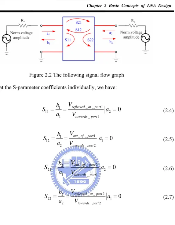
Figure 2.2 The following signal flow graph………6
Figure 2.3 A two-port network with general source and load impedance………..7
Figure 2.4 (a) Signal versus smaller noise figure, and (b) signal versus larger noise figure………...8
Figure 2.5 Frequency spectrum of input, output of the nonlinear system……….10
Figure 2.6 Inter-modulation in a nonlinear system………....11
Figure 2.7 The effect of the inter-modulation distortion in the frequency domain...12
Figure 2.8 (a) The linear gain (α1A) and the nonlinear component (3α3A3 /4 ); (b) The input and output third order intercept point (IIP3, OIP3)……….13
Figure 2.9 Illustration of the 1-dB compression point………..14
Figure 2.10 Illustration of the P1dB small………..15
Figure 2.11 Illustration of the P1dB large………..….15
Figure 2.12 Traditional transistor-amplifier of input matching………...16
Figure 2.13 Resistive termination matching technique………...16
Figure 2.14 Common gate input matching technique……….….17
Figure 2.15 Shunt series resistor feedback matching technique………..18
Figure 2.16 Inductive source degeneration matching technique………...…..18
Figure 2.17 Equivalent circuit of inductive source degeneration matching……....19
Figure 2.18 LNA with an external capacitor (CE)………...22
Figure 2.19 LNA exploiting noise canceling with a plus adder………..23
Figure 2.20 LNA with gate-drain overlap capacitance………..….24
Figure 2.21 On-chip Planner Spiral Inductors of different shapes………..…25 Figure 3.1 Proposed Common-Gate UWB LNA, which is filter configuration…27
Figure 3.2 Common gate LNA input stage, which 2nd band-pass filter, and small
signal equivalent circuit model……….28
Figure 3.3 Reflection coefficient and gain response of 2nd band-pass filter……..29
Figure 3.4 The smith chart of input reflection coefficient with 2nd band-pass filter ………..30
Figure 3.5 (a) Proposed low power LNA, and (b) π-section LC network of proposed LNA………..31
Figure 3.6 π-section small signal equivalent circuit model………...…31
Figure 3.7 Reflection coefficient of π-section with different inductor L2……….32
Figure 3.8 Power gain versus signal frequency with L2………33
Figure 3.9 Input impedance of typical common gate LNA………...33
Figure 3.10 A flow chart of proposed low direct current design……….34
Figure 3.11 The impedance transformations technique with using band pass filter ………..35
Figure 3.12 (a) Conventional cascode architecture LNA, (b) Low voltage LC tank cascade LNA………35
Figure 3.13 (a)The allowable voltages, and (b) low voltage design of the cascode architecture LNA………..36
Figure 3.14 Layout of the proposed UWB LNA…...38
Figure 3.15 Measure PCB of the proposed UWB LNA……….…….38
Figure 3.16 S-parameters versus signal frequency……….….39
Figure 3.17 Noise figure versus signal frequency with or without Rb…..………...39
Figure 3.18 Linearity parameters P1dB at 3GHz………...41
Figure 3.19 Linearity parameters OIP3 at 3GHz……….41
Figure 3.20 Linearity parameters P1dB at 4GHz………...42
Figure 3.21 Linearity parameters OIP3 at 4GHz……….42
Figure 3.22 Linearity parameters P1dB at 5GHz……… ………..43
Figure 3.23 Linearity parameters OIP3 at 5GHz……….43
Figure 3.25 Linearity parameters OIP3 at 6GHz……….44
Figure 3.26 Linearity parameters P1dB at 7GHz…..……….45
Figure 3.27 Linearity parameters OIP3 at 7GHz….….………...45
Figure 3.28 Linearity parameters P1dB at 8GHz……..……….46
Figure 3.29 Linearity parameters OIP3 at 8GHz..………….………..…46
Figure 3.30 Linearity parameters P1dB at 9GHz…..……….47
Figure 3.31 Linearity parameters OIP3 at 9GHz….….………...47
Figure 3.32 Linearity parameters P1dB at 10.6GHz……..………48
Figure 3.33 Linearity parameters OIP3 at 10.6GHz..……….48
Figure 4.1 Conventional narrowband cascode LNA……….50
Figure 4.2 The proposed ultra-wideband LNA, which is resistor feedback configuration………50
Figure 4.3 The smith chart of input impedance matching (Rf=1000Ω)………….52
Figure 4.4 Bandwidth with Rf=1000Ω to compare with the case without Rf…....52
Figure 4.5 Noise equivalent circuit of the input stage of proposed ultra-wideband LNA………..53
Figure 4.6 Noise Figure versus Frequency (Formulated and Simulated)………..57
Figure 4.7 Theoretical predictions of Noise Figure for several power dissipations.………..57
Figure 4.8 Equivalent circuit model of the substrate with an added resistor Rbx, which is located between the body node and the source node of transistor, and Rb, Rsb, Rdb represent the effective substrate model…..58
Figure 4.9 The small-signal equivalent circuit for substrate model with add resistor (Rbx)……….59
Figure 4.10 Noise equivalent circuit for LNA with substrate noise………....60
Figure 4.11 Noise Figure versus Resistor Rbx………...63
Figure 4.13 Noise Figure versus signal frequency with Rbx=10kΩ to compare with
the case without Rbx………..64
Figure 4.14 Linearity parameters P1dB at 6GHz……….…..65
Figure 4.15 Linearity parameters OIP3 at 6GHz ………65
Figure 4.16 Linearity parameters P1dB at 7GHz………...66
Figure 4.17 Linearity parameters OIP3 at 7GHz ………....66
Figure 4.18 Linearity parameters P1dB at 8GHz………...67
Figure 4.19 Linearity parameters OIP3 at 8GHz ………..…..67
Figure 4.20 Linearity parameters P1dB at 9GHz……….68
Figure 4.21 Linearity parameters OIP3 at 9GHz ………..68
Figure 4.22 Linearity parameters P1dB at 10GHz………...69
Figure 4.23 Linearity parameters OIP3 at 10GHz ………....69
Figure 4.24 NMOS I/V characteristic………....70
Figure 4.25 Depletion region and Inversion region (saturation region) with (a) VGS<Vth, (b) VGS
≥
Vth of NMOS transistors……….71Figure 4.26 VGS (min Vth) with or without VBS………...71
Figure 4.27 Threshold voltage Vth as a function of external bias VBS………....…72
Figure 4.28 Device I-V Curves without external bias VBS……….…72
Figure 4.29 Device I-V Curves with external bias VBS=0.6……….……..73
Figure 4.30 Proposed UWB LNA with Low voltage design.………...73
Figure 4.31 S-parameters versus signal frequency………...75
Figure 4.32 Power gain versus signal frequency with Low voltage design……...75
Figure 4.33 Noise figure versus signal frequency with or without Low voltage design………...75
Chapter 1 Introduction
Chapter 1 Introduction
1.1 Background and Problems
Ultra-wideband (UWB) communication techniques have attracted great interests in both academia and industry in the past few years for applications in short-range and high-speed wireless mobile system. The Federal Communication Commission (FCC) has recently approved the 3.1GHz to 10.6GHz band for UWB deployment as shown in Figure 1.1. Due to the U-NII bands (5.15GHz-5.85GHz in the United States and 4.9GHz-5.1GHz in Japan (GROUP B)) to lie in the middle of the allocated spectrum, the UWB spectrum is broken into two distinct and orthogonal bands that are free from interference: 3.1GHz-4.8GHz and 6.0GHz-10.6GHz. We subsequently refer to these two bands as the lower and upper UWB bands, respectively.
Chapter 1 Introduction
Figure 1.1 Multi-Band OFDM Proposal
A LNA is the first stage, after antenna in the receiver block of a communication system. It is widely used in the front end of narrow band communication system. For UWB applications, which ranges from 3.1GHz to 10.6GHz, because transmitted power spreads over a wide range and is restricted to be less than -41.3 dBm per MHz. There are several common goals in the design of UWB LNA including input impedance matching, low power consumption, low noise performance, small sizes, sufficient linearity, and enough power gain to overcome the noise of subsequent stages. The thesis starts with a deep analysis of the noise figure, wideband, and flatness gain problems, and reviews recently-published literatures thoroughly. After that, we try to find new ways of achieving these goals.
The thesis firstly proposes a new UWB LNA architecture, which incorporates a filter architecture and feedback resistor to enhance the bandwidth. The proposed LNA architecture covers from 3GHz to 11GHz, and shows low power consumption, and much better power gain flatness. Secondly, a novel low voltage design method is proposed for a common-source UWB LNA to attain very low power consumption.
1.2 Related Works
Chapter 1 Introduction
communication applications. The well-developed distributed amplifier is known as its wide bandwidth, but it requires large power consumption and layout area [8]. The filter design technique and source inductor degeneration technique are employed to incorporate the transistor gate-source capacitance as a part of the LC-ladder matching network and extend the bandwidth to a wide range [1], [7], [10], [13]-[17]. A common gate (or the 1/gm termination) amplifier has the highest potential to achieve the wideband input matching, good linearity, and input-output isolation, but it leads to lower gain and higher noise figure than using a common source amplifier [3]. Only a few literatures have reported on the design of a common gate LNA [3], [4], [5].
1.3 Thesis Organization
The thesis is organized into five chapters including the introduction. Chapter 2 deals with the receiver basics and basic concepts of low noise amplifier design, its metrics and some popular LNA topologies with their comparison. Chapter 3 proposes ultra-wideband LNA of proposed low power design with simulation results. In chapter 4, the noise analysis of the UWB LNA, and low voltage LNA design. In Chapter 5, conclusion is drawn.
Chapter 2 Basic Concepts of LNA Design
Chapter 2 Basic Concepts of Low Noise Amplifier
Design
2.1 System Specifications of the LNA
2.1.1 S-Parameters
Scatter Parameters, also called S-parameters, belong to the group to two-port parameters used in two port theory [47]-[50]. S-parameters are important in microwave design because they are easier to measure and to work with at high frequencies than other kinds of two-port parameters. The S-parameters are defined as:
2 2 2 2 1 11 12 1 2 2 2 2 2 21 22 2
*
b
S
S
a
b
S
S
a
⎛
⎞ ⎛
⎞ ⎛
⎞
⎜
⎟ ⎜
=
⎟ ⎜
⎟
⎜
⎟ ⎜
⎟ ⎜
⎟
⎝
⎠ ⎝
⎠ ⎝
⎠
(2.1) 2 ia : Power wave traveling towards the two-port gate
2
i
b
: Power wave reflected back from the two-port gate2 11
Chapter 2 Basic Concepts of LNA Design
2 12
S : Power transmitted from port 1 to port 2
2 21
S : Power transmitted from port 2 to port 1
2 22
S : Power reflected from port 2
Since the two-port is imbedded in a characteristic impedance of Z0, these 'waves' can
be interpreted in terms of normalized voltage or current amplitudes. This is explained in Figure 2.1. In other words, we can convert the power towards the two-port into a normalized voltage amplitude of
_
0
towards two port i
V
a
Z
−=
(2.2)and the power away from the two-port can be interpreted in terms of voltages like
_ _
0
away from two port i V b Z − = (2.3)
Figure 2.1 S-Parameters and Characteristic Impedance Z0
The following signal flow graph gives the situation for the S-parameter interpretation in voltage as shown in Figure 2.2.
Chapter 2 Basic Concepts of LNA Design
Figure 2.2 The following signal flow graph Looking at the S-parameter coefficients individually, we have:
_ _ 1 1 11 2 1 _ 1
0
reflected at port towards portV
b
S
a
a
V
=
=
=
(2.4) _ _ 1 1 12 1 2 _ 20
out of port towards portV
b
S
a
a
V
=
=
=
(2.5) _ _ 2 2 21 2 1 _ 10
out of port towards portV
b
S
a
a
V
=
=
=
(2.6) _ _ 2 2 22 1 2 _ 2 0 reflected at port towards port V b S a a V = = = (2.7)2.1.2 Power Gain
In this section we develop several expressions for the power gain of a general two-port amplifier circuit in terms of the S-parameters of the amplifier.
Definitions of Two-Port Gains:
Consider an arbitrary two-port network [S] connected to source and load impedances Zs and ZL, respectively, as shown in Figure 2.3. We will derive expressions
for three types of power gain in terms of the S parameters of the two-port network and the reflection coefficients, Γ and S Γ of the source and load [47]-[50]. L
Chapter 2 Basic Concepts of LNA Design
Figure 2.3 A two-port network with general source and load impedance
z Power Gain = G = PL/Pin is the ratio of power dissipated in the load ZL to the
power delivered to input of the two-port network. This power gain is independent of ZS, although some active circuits are strongly dependent on ZS.
(
)
(
)
2 2 21 2 2 22 1 1 1 L L in in L S P G P S − Γ = = − Γ − Γ (2.8)z Available Gain = GA = PAVN/PAVS is the ratio of the power available from the
two port network to the power available from the source. This assumes conjugate matching of the both the source and the load, and depends on ZS but
not ZL.
(
)
(
)
2 2 21 2 2 11 1 1 1 S AVN A AVS out L S P G P S − Γ = = − Γ − Γ (2.9)z Transducer Power Gain = GT = PL/PAVS is the ratio of the power delivered to the
load to the power available from the source. This depends on both ZS and ZL .
(
)(
)
2 2 2 21 2 2 22 1 1 1 1 L S L T AVS S in L S P G P S − Γ − Γ = = − Γ Γ − Γ (2.10)A special case of the transducer power gain occurs when both the input and output are matched foe zero reflection. Then Γ = Γ =0, and equation (2.10) can given
Chapter 2 Basic Concepts of LNA Design by:
G
T=
S
212 (2.11) Where 12 21 11 221
L in LS S
S
S
Γ
Γ =
+
−
Γ
(2.12) 12 21 22 111
S out SS S
S
S
Γ
Γ =
+
− Γ
(2.13) SΓ , Γ are the designed input and output matching points, respectively. L
2.1.3 Noise Figure (NF) of LNA
In Figure 2.4, we can indicate the input signal by drawing a simple diagram as follows: If low noise amplifier has smaller noise figure, the output signal has a little distortion. Oppositely, low noise amplifier has larger noise figure, the output signal has a great deal distortion. Two methods for analyzing the effect of noise in electronic devices and LNA circuits [49] are illustrate in Appendix A.
Figure 2.4 (a) Signal versus smaller noise figure, and (b) signal versus larger noise figure
Chapter 2 Basic Concepts of LNA Design
2.1.4 Sensitivity
In wireless communication systems, the definition of sensitivity is limited by noise figure. The sensitivity of RF front end receiver is defined as the minimum signal level that the system can detect with acceptable signal-to-noise ratio [48]. Sensitivity determines the maximum distance that a receiver can be away from the transmitter or the base station for a mobile phone case. Its can be specified in the unit of dBm (decibels relative to one milli-watt) along with the reference impedance (50Ohm for most systems) and is typically measured in the interference-free environment. Usually, the minimal detect signal power can be written as
, min min
10log
in dBm rs dBm Hz dB dBm
P
=
P
+
NF
+
SNR
+
B
, (2.14)where NF is the noise figure of the receiver system, B is the signal channel bandwidth, SNRmin is the minimal acceptable signal-to-noise ratio. Assuming conjugate matching at
the output, we can obtain Prs as the noise power that source resistance delivers to the
receiver. 4 1 174 ( ) 4 s rs s in in kTR P kT dBm Hz R R R = = = − = (2.15)
Assuming equation (2.47) at room temperature, its can be written as
, min
174
10log
minin dBm
P
= −
dBm Hz
+
NF
+
B
+
SNR
(2.16)2.1.5 Harmonics
The input-output relationship of a nonlinear system:
2 3
1 2 3
( )
( )
( )
( )
Chapter 2 Basic Concepts of LNA Design
generated. Using the input-output relationship (2.17) with a signal tone at the input s(t)=Acosω0 t, the output of the nonlinear systems can be viewed mathematically as
2 2 3 3 1 0 2 0 3 0 3 3 2 2 3 3 2 2 1 0 0 0
( ) cos cos cos
3
cos cos 2 cos 3
2 4 2 4 y t A t A t A t A A A A A t t t α ω α ω α ω α α α α ω α ω ω = + + ⎛ ⎞ = +⎜ + ⎟ + + ⎝ ⎠ (2.18)
Harmonic distortion is defined as the ratio of the amplitude of a particular harmonic to the amplitude of the fundamental. For example, third-order harmonic distortion (HD3)is defined as the ratio of amplitude of the tone at 3ω0 to the amplitude of the fundamental
at ω0 applying this definition to (2.18), we have
2 3 3 1
1
4
HD
α
A
α
=
(2.19)Next, we take the Fourier transform of (2.18):
[
]
[
]
[
]
3 2 3 2 1 0 0 2 2 0 0 3 3 0 0 3 ( ) ( ) ( ) ( ) 4 ( 2 ) ( 2 ) 2 ( 3 ) ( 3 ) 4 A Y A A A A α ω α πδ ω π α δ ω ω δ ω ω α π δ ω ω δ ω ω α π δ ω ω δ ω ω ⎛ ⎞ = + ⎜ + ⎟ − + + ⎝ ⎠ + − + + + − + + (2.20)Equation (2.20) is plotted in Figure 2.5.
Figure 2.5 Frequency spectrum of input, output of the nonlinear system
2.1.6 Inter-Modulation
Chapter 2 Basic Concepts of LNA Design
two strong interferers occur at the input of the receiver, specified by s(t)= A1cosω1t+
A2cosω2t. The inter-modulation distortion can be expressed mathematically by applying
s(t) to (2.17):
(
)
(
)
(
)
2 1 1 1 2 2 2 1 1 2 2 3 3 1 1 2 2( ) cos cos cos cos
cos cos y t A t A t A t A t A t A t α ω ω α ω ω α ω ω = + + + + + (2.21)
Using trigonometric manipulations, we can find expressions for the second and the third-order inter-modulation products as follows:
(
)
(
)
1 2: 2 1 2A A cos 1 2 t 2 1 2A A cos 1 2 t; ω ω α± ω ω+ +α ω ω−(
)
(
)
2 2 3 1 2 3 1 2 1 2 1 2 1 2 3 3 2 : cos 2 cos 2 ; 4 4 A A A A t t α α ω ω± ω ω+ + ω ω−(
)
(
)
2 2 3 2 1 3 2 1 2 1 2 1 2 1 3 3 2 : cos 2 cos 2 . 4 4 A A A A t t α α ω ω± ω ω+ + ω ω− (2.22)The third-order inter-modulation products at 2ω2-ω1, 2ω1-ω2 and a nonlinear system
(ex: LNA, PA..), the output signal will be corrupted are illustrated in Figure.2.6.
Figure 2.6 Inter-modulation in a nonlinear system
The output spectrum in the frequency domain can be determined from (2.22) by evaluating its Fourier transform Y(ω). This is shown in Figure 2.9, where the following signals: ω0: desired signal, ω1, ω2: strong interferers, 2ω1, 2ω2: harmonics of the
interferers, ω1±ω2: second order inter-modulations products, 2ω1,2±ω2,1: Third order
Chapter 2 Basic Concepts of LNA Design
Furthermore, ω1, ω2 are close to ω0 ; therefore, trying to filter them out requires a filter
bandwidth that is very narrow and is impractical. Keeping down 2ω2-ω1 by keeping the
nonlinearity small is the only solution.
Figure 2.7 The effect of the inter-modulation distortion in the frequency domain
2.1.7 Third Order Harmonics Intercept Point (IP3)
From (2.21), we note that as the input level A increase, the desired signal at the output is proportional to A (by the small signal gain α1). On the other hand, from (2.22) we can
see that the third-order product increases in proportion to A3. This is plotted on a linear scale in Figure 2.8 (a). Figure 2.8 (a) is re-plotted on a logarithmic scale in Figure 2.8 (b), where power level is used instead of amplitude level. As shown in Figure 2.10 (b), the third-order intercept point IP3 is defined to be the intersection of the two lines. From Figure 2.8 (b), we can see that the amplitude of the input interferer at the third-order intercept point, AIP3, is defined by the relation
(
)
3 3 1 3 3 3 20log 20log 4 IP IP A α A α = ⎛⎜ ⎞⎟ ⎝ ⎠ (2.23) From (2.23), we can solve for AIP3:1 3 3 4 3 IP A
α
α
= (2.24)Chapter 2 Basic Concepts of LNA Design
A2IP3/50Ω.(IIP3 is hence interpreted as the power level of the input interferer for a 50Ω
load at the third-order intercept point).
Figure 2.8 (a) The linear gain (α1A) and the nonlinear component (3α3A3 /4 ); (b) The
input and output third order intercept point (IIP3, OIP3)
2.1.8 1-dB Gain Compression Point (P1dB)
When the input signal to an amplifier is large, the amplifier will be saturates, hence clipping the signal. When the strength of the input signal is further increased, the output signal is no longer amplified. At this point, the output is said to be compressed. From (2.17), we observe that in y(t) there are two terms with frequency ω0 due to the
nonlinear behavior. Assume that the other terms in y(t) have frequency outside the band of interest and hence are removed by the BPFs. Thus, y(t) becomes
3 2 3 3 1 0 1 0 3 3 ( ) cos cos 4 4 A A y t =⎜⎛α A+ α ⎞⎟ ωt=⎛⎜α + α ⎟⎞A ωt ⎝ ⎠ ⎝ ⎠ (2.25)
In the case where α3 is negative, the second term is decreasing the gain. As the input
Chapter 2 Basic Concepts of LNA Design
signal when the linear voltage gain drops by 1dB. Form (2.25), we see that the 1-dB compression point can be expressed mathematically by
2 3 1 1 1 3 1 4 dB dB dB A dB
α
α
−α
⎛ ⎞ + = − ⎜ ⎟ ⎝ ⎠ (2.26)We can rewrite (2.26) in terms of decibels:
2
3 1 1
1 1
3
20 log 20 log 20 log1.122 20 log
4 1.122
dB
A
α α
α + − = α − = (2.27)
From (2.27), the A1-dB input level is given by
1 1 3 0.145 dB A α α − = (2.28)
The ideal of the 1dB compression point is shown graphically in Figure 2.9. In
Figure 2.9 Illustration of the 1-dB compression point
Figure 2.10 illustrates that when input signal is -20dBm, gain is 10dB, and P1dB is
0dBm, the output signal will be -20dBm+10=-10dBm. Due to output signal < P1dB=
0dBm, so the output signal will not distortion. Oppositely, if input signal is -5dBm, the output signal will be -5dBm+10=+5dBm. But the output signal over the P1dB= 0dBm, so
Chapter 2 Basic Concepts of LNA Design
the output signal will distortion. In Figure 2.11 illustrates that P1dB large when input signal is -20dBm or -5dBm, the output signal will not distortion.
Figure 2.10 Illustration of the P1dB small
Figure 2.11 Illustration of the P1dB large
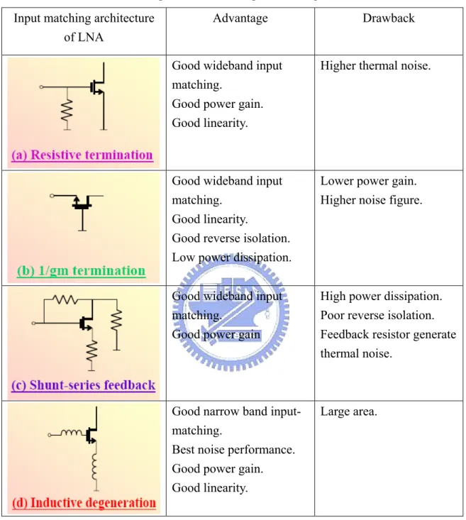
2.2 Conventional LNA input matching Architecture
Chapter 2 Basic Concepts of LNA Design
amplify the received weak RF signal with the minimum noise figure. Between the wideband input matching and the noise figure of the UWB LNA should be carefully studied and decide. Impedance matching is very important in LNA designs. There are four basic 50Ohm input matching architectures that have been explored in the traditional transistor-amplifier shown in Figure 2.12. In this section, we will investigate a number of circuit architecture that can be used of the task and discussed.
Figure 2.12 Traditional transistor-amplifier of input matching
a.
Resistive Termination architecture
Resistive termination architecture is the most straightforward approach to achieve the wideband 50Ohm matching at the input as shown in Figure 2.13. The 50Ohm resistor (R) is placed across the input terminal of the LNA and hence providing a wideband matching.
Figure 2.13 Resistive termination matching technique
The bandwidth of this matching technique is determined by the input capacitance of the transistor M1 and can be very high. However, the resistor R adds into circuit will
Chapter 2 Basic Concepts of LNA Design
good input matching, but leads to high thermal noise in circuit. If ignoring all the noises from the transistors, the lower bound of the noise factor is equal to 2. Hence, the resistor termination technique is not practical in most application.
b.
Common Gate input architecture (1/gm termination)
The last input matching method is to use a common-gate architecture as shown in Figure 2.16. [3], [4], [12]. A common gate (or the 1/gm termination) architecture has the highest potential to achieve the wideband input matching, good linearity, and input-output isolation, but it leads to lower gain and higher noise figure than using the other mentioned techniques. Using the common gate architecture has the lower bound noise factor is
F
1
γ
α
≈ +
≧2.2. (i.e Long channel F=2.2, Short channel F=4.7~6).Figure 2.14 Common gate input matching technique
c.
Shunt-Series resistor feedback architecture
The resistor feedback technique is used for getting a good input matching architecture as shown in Figure 2.15 [9], [14], [21], [22], [23], [25]. This technique unlike resistive termination case, it does not attenuate the signal by a noisy attenuator before reaching the gate of amplifying device and hence the noise figure is expected to be much higher. However, the feedback resistor (RF) continues to generate thermal noise
Chapter 2 Basic Concepts of LNA Design
Figure 2.15 Shunt series resistor feedback matching technique
d.
Inductive Source Degeneration architecture
The inductive source degeneration architecture is popular with input matching technique of LNA. [1], [5]-[7], [10], [13]-[18], [24], [26]-[30]. This matching technique provides a perfect matching without adding any noise to the system or giving any restrictions on the device gm. It uses an inductor as a source degeneration device and has
another inductor connecting to the gate as shown in Figure 2.16.
Figure 2.16 Inductive source degeneration matching technique
Using the small signal analysis and neglecting Cgd of transistor M1, the impedance
looking through the gate inductor can be written as:
1
(
)
in g s T s gsZ
j
L
L
L
j C
ω
ω
ω
=
+
+
+
(2.29)Chapter 2 Basic Concepts of LNA Design Where m T gs g C
ω
= (2.30)At the resonance frequency where the inductor impedance and capacitor impedance are canceled out, the input impedance is then just the last term in the equation (2.29). The tuned impedance is given by:
0
( )
in eq T sZ
ω
=
R
=
ω
L
(2.31) Where 0 1 (Lg L Cs) gs ω = + (2.32)In Figure 2.17 shows the equivalent model of the inductive source degeneration architecture, the quality factor of the circuit is given by:
gs eq
C
Q
R
ω
=
(2.33)The effectively increase the transconductance of the input transistor by a factor can written as
G
m=
Qg
m. In typical narrow band matching, the quality factor is usually around 3-5. Assuming that the matching network is lossless, helps to reduce the input-referred added noise by a factor of Q as well as increasing the voltage gain of the circuit by the same factor.Chapter 2 Basic Concepts of LNA Design
e. LNA design and comparison of input matching architecture
In general, the following should be considered in LNA design:
a. Input and Output matching (return loss): In wireless receiver, the component placed before LNA is usually the filter and antenna with characteristic impedance 50Ω, so input impedance matching of LNA must be matching to close to 50Ω. But, the input impedance matching is always different from the optimum noise matching.
b. Low Noise Figure (NF): The low noise figure of the LNA is dominates all noise figure of the entire receiver system. Thus, noise figure of LNA is the most important parameters to evaluate the performance. The low noise figure and low power dissipation are well-known that two issues are trade-offs one another.
c. Sufficient power gain: The sufficient power gain of the LNA is important, because it amplify the receiver RF signal and reduce the noise contribution from the following stages. But, the larger power gain will degrade the linearity of LNA.
d. Low power dissipation: Design a wide band low noise amplifier, the low power issue is important, but it trade off with noise figure and power gain.
Chapter 2 Basic Concepts of LNA Design
Table 2.1 Comparison of LNA input matching architecture Input matching architecture
of LNA
Advantage Drawback
Good wideband input matching.
Good power gain. Good linearity.
Higher thermal noise.
Good wideband input matching.
Good linearity.
Good reverse isolation. Low power dissipation.
Lower power gain. Higher noise figure.
Good wideband input matching.
Good power gain
High power dissipation. Poor reverse isolation. Feedback resistor generate thermal noise.
Good narrow band input- matching.
Best noise performance. Good power gain. Good linearity.
Chapter 2 Basic Concepts of LNA Design
2.3 Methods to Reduce Noise Figure of LNA
Due to the various requirements of low noise amplifiers, the low noise characteristic. There are several methods to reduce the noise figure were proposed[6], [14], [31], [34].
2.3.1 External gate-source capacitor method
Since the induced gate current noise grows with the gate-source capacitance (Cgs),
the addition gate-source capacitor (CE) can reduce the noise figure from the induced
gate current noise by reducing Cgs. The input stage of LNA with an external capacitor
(CE) is shown inFigure 2.18.
Figure 2.18 LNA with an external capacitor (CE)
The input impedance of circuit inFigure 2.20 can be given by:
1
(
)
(
)
m s in g s E gs E gsg L
Z
s L
L
s C
C
C
C
=
+
+
+
+
+
(2.34)The quality factor Q of the input circuit is:
0 0 1 1 2 ( ) ( m s ) ( ) s E gs s E gs E gs Q g L R C C R C C C C
ω
ω
= = + + + + (2.35)The noise figure can be derived as[1]
2 2 2 2 2 1 1 ( )( ) 4 4 4 1 gs m gs m dn E gs dn E gs out C g C g Q g c C C g C C R F R Q g
γ
βγ
β
+ + + + + + = + (2.36)Chapter 2 Basic Concepts of LNA Design
From equation(2.36), the value of Q from Cgs allows for an adjustable Q for any given
Cgs to reduce the noise figure[1].
2.3.2 Thermal noise canceling method
Figure 2.19 illustrates that a thermal noise canceling method with straightforward implementation using an ideal feed-forward voltage amplifier A with a gain -Av (with
Av>0) [6].
Figure 2.19 LNA exploiting noise canceling with a plus adder By circuit inspection, the matching device noise voltages at node X and Y are
, , , , , ,
( ,
)
( ,
)
(
)
X n i s mi n i s Y n i s mi n i sV
R g
I R
V
R g
I
R
R
α
α
=
=
+
(2.37)The output noise voltage due to the noise of the matching device, Vout,n,i is then equal to
, , , , , , ,
.
( ,
)
(
)
out n i Y n i X n i V s mi n i s V sV
V
V
A
R g
I
R
R
A R
α
=
−
=
+ −
(2.38)Output noise cancellation, Vout,n,i=0, is achieved for a gain AV equal to
, , , ,
1
Y n i V X n i sV
R
A
V
R
=
= +
(2.39)Chapter 2 Basic Concepts of LNA Design
2.3.3 Gate-drain overlap capacitance neutralization method
The feedback from the gate-drain overlap capacitance (Cgd) can not be ignored in
the high frequency, which leads to input matching and gain degradation. To reduce the feedback effect is by using cascade architecture, which leads to low voltage technique. The inductor-tuned technique can be implemented as shown in Figure 2.20.
Figure 2.20 LNA with gate-drain overlap capacitance
It may not be suitable for on-chip implementations because the required inductance to resonant the Cgd is quite large for on-chip integration.
2.3.4 Quality factor (Q) of inductor enhancement method
Integrated high-Q inductors can improve the performance and integration-level of RFIC’s while reducing their power dissipation and cost. Poor quality factors of on-chip matching inductors are affects the noise at high frequency. A new implementation of high quality factor (Q) copper inductor on CMOS silicon substrate using a fully process is presented. The Q factor of such inductors depends upon the conductivity of metal layer and other parasitic components. Planner spirals can be of different shapes i.e. square, hexagonal, octagonal and circular as shown in Figure 2.21.
Chapter 2 Basic Concepts of LNA Design
Chapter 3 Design of the Lower Power Ultra-Wideband LNA
Chapter 3 Design of the Low Power Ultra-Wideband
Low Noise Amplifier
3.1 Introduction
In this chapter, instead of using a common source amplifier, a common-gate amplifier is proposed for wideband input matching of UWB LNAs. It is well known that compared with using the common source amplifier, using the common gate amplifier can easily achieve wideband input matching, good linearity, and input-output isolation, but provides lower gain and higher noise figure. The π-section LC network technique is employed in the LNA to achieve sufficient gain with a reasonable noise figure level. The gain flatness throughout the band is within ± 1.0dB. Here, we also propose a structure to combine the common gate with band pass filters, which can reduce parasitic capacitance of the transistor and leads low power consumption.
3.2 Proposed Low Power UWB LNA architecture
Chapter 3 Design of the Lower Power Ultra-Wideband LNA
reasonable power gain, are the major issues to be considered in the circuit design. It is well-known that these four issues are trade-offs one another [44]. Here, achieving optimum low power performance is our first priority. Our proposed UWB LNA circuit is shown in Figure 3.1, which employs the CMOS process. The LNA is composed by an input matching network and a π-section LC network.
Figure 3.1 Proposed Common-Gate UWB LNA, which is filter configuration
3.2.1 Wideband Input Matching Design
Here, a common-gate amplifier is used as an important component for the input matching network of the proposed LNA. Although the common gate amplifier can easily achieve wideband input matching, good linearity, and input-output isolation, its parasitic capacitances of the transistor, will degrade the LNA performance in the high frequency region. Therefore, a two-order band pass filter is also introduced to reduce the parasitic capacitance. Demonstrates the proposed input matching network, which is composed of a common gate amplified and a two-order band pass filter, and its small signal equivalent circuit model are shown in Figure 3.2.
Chapter 3 Design of the Lower Power Ultra-Wideband LNA
Figure 3.2 Common gate LNA input stage, which 2nd band-pass filter, and small signal equivalent circuit model
In the equivalent circuit (Figure 3.2), ZL is the input impedance of the cascode
stage and gm1 is the transconductance of the MOS transistor in common gate
configuration, Ro is the parasitic resistance of the transistor. L1, C1, Ls, and C2+Cgs are
lumped-element circuits for the two order band-pass filter. Series and shunt L-C tanks are used to adjust the pass band and the ripple. Based on band pass filter design fundamental[43], L1, C1, Ls, and C2+Cgs are given by, respectively,
0 1 1 1 0 1 0 0 Z g L C g Z ω ω Δ = = Δ (3.1) 2 0 2 0 0 2 0 S gs g Z L C C g Z ω ω Δ = + = Δ (3.2)
Here, Δ=(ω2-ω1)/ω0 is the fractional bandwidth of the filter. ω2 and ω1 are the upper
(10.6GHz) and lower (3.1GHz) frequencies of the pass band. g1 and g2 are two
empirical constants and are equal to 1.5963 and 1.0967, respectively [43]. The matching network is adopted for noise and impedance match to the 50 Ohm source with
Chapter 3 Design of the Lower Power Ultra-Wideband LNA
L1=0.9nH, C1=850fF, Ls=3.50nH, C2+Cgs=240fF, which reflection coefficient and gain response simulation shown in Figure 3.3.
Figure 3.3 Reflection coefficient and gain response of 2nd band-pass filter
With the small signal equivalent circuit model (Figure 3.2), the input impedance of the MOS transistor can be treated as a series RLC circuit and is written as below:
1 1 1 1 1 1 1 1 1 ( ) 1 ( ) ( ) in m m S o Z j L g Z j C g Z R Z
ω
ω
ω
ω
ω
= + + − + + + (3.3), where Zs(ω) and Z1(ω) are given by (1) and (2) below, respectively.
1 ( ) 1 S gs S Z j C j L ω ω ω = + (3.4) 1 1 ( ) 1 gd L Z j C Z ω ω = + (3.5)
From the smith chart in Figure 3.4, shows the reflection coefficient S11 of the proposed low power UWB low noise amplifier with a structure to combine the common gate with band pass filters and compares that of the amplifier without band pass filters. The addition of band pass filters gathers the values of input reflection coefficient S11
Chapter 3 Design of the Lower Power Ultra-Wideband LNA
coefficient with feedback circuit for frequency range is close to 50Ω matching.
Figure 3.4 The smith chart of input reflection coefficient with 2nd band-pass filter
3.2.2 π-section LC network Design
Flat gain over the entire bandwidth, is another important requirement of the UWB LNA design. However, the shunt of M1’s gate-drain parasitic capacitance, Cgd1 , and
M2’s gate-source parasitic capacitance, Cgs2 , provides an additional path for the RF
signal current to the ground, which leads to power gain reduction especially for the high frequency band. In order to solve this problem, a π-section LC network technique is first adopted and proposed for our design. Figure 3.5 (b) shows the circuit of the π-section LC network, which is formed by an inductor and the gate-source parasitic capacitances. The small signal equivalent circuit of the π-section LC network circuit is illustrated in Figure 3.6. Id1 is the small signal drain current of M1. L2 is the introduced passive
inductor. Ro and Co represent the parasitic resistance and capacitance of the inductor,
respectively. Ro is the series resistance and is around 3 to 20 Ohms, and Co is the
Chapter 3 Design of the Lower Power Ultra-Wideband LNA
Figure 3.5 (a) Proposed low power LNA, and (b) π-section LC network of proposed LNA.
Figure 3.6 π-section small signal equivalent circuit model
After some derivations, the π-section LC network circuit gain, Vd1/Id1, is found and
given by 1 1 1 2 1 2 2 2 1 ( ) 1 1 1 ( ) ( ) 1 ( ) d d gd o sub sub gs o o V I j C j L R Z Z j C j C j L R ω ω ω ω ω ω ω ω = + + + + + + + (3.6)
, where Zsub1(ω) and Zsub2(ω) are given by (3.7) and (3.8), respectively.
1 1 1 1 1 1 ( ) 1 sub ox sub sub Z j C j C R
ω
ω
ω
= + + (3.7)Chapter 3 Design of the Lower Power Ultra-Wideband LNA 2 2 2 2 1 1 ( ) 1 sub ox sub sub Z j C j C R
ω
ω
ω
= + + (3.8) Here Cox , Rsub, and Csub are ignored in equation (3.6), where Cox is the oxidecapacitance between the spiral and the substrate. Rsub, and Csub are silicon substrate
resistance and silicon substrate capacitance, respectively, which are relatively small and are neglected. Then, equation (3.6) becomes
1 1 1 2 2 2 1 ( ) 1 1 1 ( ) d d gd o gs o o V I j C j L R j C j C j L R
ω
ω
ω
ω
ω
ω
= + + + + + (3.9)Z(ω)=Vd1/Id1 is the input impedance of π-section LC network. To achieve a flat gain,
finding a proper L2 is needed to make Z(ω) close to 50 Ohm through out the whole band.
From the smith chart in Figure 3.7, shows the reflection coefficient of π-section input reflection coefficient with different inductor L2..
Figure 3.7 Reflection coefficient of π-section with different inductor L2.
It is found from Figure 3.8 that L2=3 nH yields a satisfied flat gain within a variation of
±1.5 dB relative to the average. Therefore, inductor L2=3 nH is chosen for later
Chapter 3 Design of the Lower Power Ultra-Wideband LNA
Figure 3.8 Power gain versus signal frequency with L2
3.2.3 Low power Design
The low dc current technique and low voltage technique are employed to attain the low power for the ultra-wideband low noise amplifier design, which used in proposed common gate LNA (chapter 3), and common source LNA (chapter 4).
A. Low direct current design
The low direct current design is used in proposed common gate UWB LNA design. The typical common gate LNA is shown in Figure 3.9.
Figure 3.9 Input impedance of typical common gate LNA The input impedance of the common gate amplifier in Figure 3.9 can be written
Chapter 3 Design of the Lower Power Ultra-Wideband LNA 1 1 in m gs Z g j C
ω
= + (3.11) The input impedance is approximately as1 1 in m Z g
≈ in the low frequency. It has to be matched to the 50Ohm. The common gate architecture (or the 1/gm termination) that is
illustrate in Figure 3.10 (a) has the highest potential to achieve the wideband input impedance Zin ≈ Ω . However, the drain current50
(
)
2 1 2 D n ox gs thn W I C V V L μ = − , transconductance (gm) m n ox
(
gs thn)
2 n ox D1 W W g C V V C I L L μ μ = − = of transistor M1 and input impedance 1 1 1 1 1 50 2 in m D n ox D Z g W I C I L μ ≈ = ∝ = Ω. If 1 1 1 2 D D I → I , the inputimpedance of transistor M2 Zin ≈50 2 =70Ω is shown in Figure 3.10 (b). In Figure
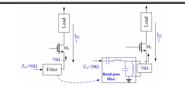
3.10 (c), we proposed a structure to combine the common gate with band pass filters technique, which can achieve the impedance transformations and leads low power consumption. The impedance transformations technique is shown in Figure 3.11 and its using two order band pass filter to achieve this design.
Chapter 3 Design of the Lower Power Ultra-Wideband LNA
Figure 3.11 The impedance transformations technique with using band pass filter
B. Low voltage design
The bottle-neck for the low voltage design is the limitation of threshold voltage because it is not anticipated to decrease much below. The conventional cascode architecture amplifier shown in Figure 3.12 (a),it require a high supply voltage and not suitable for low voltage application. In order to overcome this problem, the cascade architecture with two LC tanks, as shown in Figure 3.12 (b). The RF signal is amplified by common-source and blocking capacitor couples the signal to common gate.
Figure 3.12 (a) Conventional cascode architecture LNA, (b) Low voltage LC tank cascade LNA.
Chapter 3 Design of the Lower Power Ultra-Wideband LNA
results in a large chip area. In order to solve this problem, a solution to the reduce threshold voltage is employed to low voltage technique. The threshold voltage problem comes from the well-known relationship as given
0
( 2
2
)
th th F BS F
V
=
V
+
γ
φ
−
V
−
φ
(3.10), where Vth0 is the value of V with Vth BS=0,
γ
is the bulk threshold parameter andF
φ is the strong inversion surface potential of the MOSFET. To reduce the threshold voltage as much as possible, we want to the bias VBS as high as possible. In Figure 3.13
(a) the allowable voltages cascode architecture with inductive source degeneration is a popular configuration for LNA design. If M1and M2 are both in saturation, then VX is
determined primarily by Vb2: VX=Vb2(=VDD)-Vgs2. For M2 to be saturated,
VDD≧Vb2(=VDD)-Vthn, that is, VDD≧Vgs1-Vthn+Vgs2-Vthn if Vb2 is chosen to place M1 at
the edge of saturation. But it has not very low voltage supply applications because the power supply must satisfy the following a requirement
V
DD+
V
SS≥
2
V
thn. The VDDand VSS are the positive and negative power supply, Vthn is the threshold voltage of the
each of the NMOS transistor.
Figure 3.13 (a)The allowable voltages, and (b) low voltage design of the cascode architecture LNA.
Chapter 3 Design of the Lower Power Ultra-Wideband LNA
The low voltage design of the cascode LNA is shown in Figure 3.13 (b). A VBS=0.6 voltage is employed to forward-bias the body-source junction of transistor M1
and M2. The VDD can be attained to 0.7V with dc current is 4.5mA. The proposed
Low-voltage technique can be explained by UWB feedback LNA architecture is taken up in the next chapter.
3.3 Simulation Results
Figure 3.14 shows the layout of the proposed UWB LNA. The size of the layout area is 0.89mm by 0.77mm including pads. And the measure PCB is shown in Figure 3.15. In Figure 3.16, S11 and S22 versus signal frequency are illustrated. It is found that the input reflection S11<-10.44dB and output matching S22<-12.05dB in the range of 3.1~10.6 GHz. The power gain (S21) is around 10.0~12.4dB. 3dB bandwidth of the LNA is 7.8 GHz and is satisfied the need of UWB. The noise figure of the LNA is shown in Figure 3.17. It is found that the noise figure is at least less than 4.4dB in 3.1~10.6GHz and its minimum value is 3.25dB at 8.5GHz. The linearity of an amplifier is traditionally described in terms of 1-dB compression point (P1dB) and third-order intercept point (IP3). However, the IP3 of the proposed LNA is not of great concern of this work due to the two reasons: Firstly, the UWB signals are intrinsically wideband signals rather than single tones in narrowband systems, which bring about the difficulty in defining the IP3 for the LNA. The simulation results also show that the output third-order-intercept points (OIP3s) are 7.669dBm at 3GHz, 5.33dBm at 5GHz, 5.09dBm at 6GHz, 4.24dBm at 8GHz, 2.23dBm at 10GHz. A low supply voltage of 1.5V is chosen, and the total power consumption is 3.0mW.
Chapter 3 Design of the Lower Power Ultra-Wideband LNA
Figure 3.14 Layout of the proposed UWB LNA
Chapter 3 Design of the Lower Power Ultra-Wideband LNA
Figure 3.16 S-parameters versus signal frequency
Chapter 3 Design of the Lower Power Ultra-Wideband LNA
The performance of the proposed LNA is summarized in Table 3.1, with comparison to other recently published ultra-wideband LNAs’ simulation results.
Table 3.1
Summary of LNA performance and comparison with published LNAs
Ref. Tech. BW (GHz) S11 (dB) Gain (dB) NF (dB) IIP3 (dBm) Power (mW) [1-a] 0.18um CMOS 2.3-9.2 <-9.9 9.3 4.0 -6.7* 9.0 [1-b] 0.18um CMOS 2.4-9.5 <-9.4 10.4 4.2 -8.8* 9.0 [8] 0.18um SiGe 0.1-11 <-12 8 2.9 -3.4# 21.6 [4] 0.18um CMOS 3.1-10.6 <-9 17.5 3.1 N/A 33.2 [10] 0.18um CMOS 2-10.1 <9.76 10.2 3.68 -1.0* 7.2 Our work 0.18um CMOS 3-10.6 <-10.4 12.4 3.25 -3.97* 3.0
Chapter 3 Design of the Lower Power Ultra-Wideband LNA
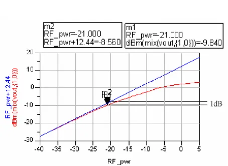
Figure 3.18 Linearity parameters P1dB at 3GHz
Linearity parameters P1dB can be explained by Figure 3.21.
P1dB=P1dB(dBm)=G1dB(dB)+IP1dB(RF_pwr)(dBm) =10+(-12)=-2dBm
Simulation results of P1dB=-3.3dBm.
Figure 3.19 Linearity parameters OIP3 at 3GHz Linearity parameters OIP3 can be explained by Figure 3.22. OIP3=Pout+1
2IMD=-10.443+ 1
Chapter 3 Design of the Lower Power Ultra-Wideband LNA
Figure 3.20 Linearity parameters P1dB at 4GHz
Linearity parameters P1dB can be explained by Figure 3.23.
P1dB=P1dB(dBm)=G1dB(dB)+IP1dB(RF_pwr)(dBm) =11.5+(-16)=-5.5dBm
Simulation results of P1dB=-5.8dBm.
Figure 3.21 Linearity parameters OIP3 at 4GHz Linearity parameters OIP3 can be explained by Figure 3.24. OIP3=Pout+1
2IMD=-9.29+ 1
Chapter 3 Design of the Lower Power Ultra-Wideband LNA
Figure 3.22 Linearity parameters P1dB at 5GHz
Linearity parameters P1dB can be explained by Figure 3.25.
P1dB=P1dB(dBm)=G1dB(dB)+IP1dB(RF_pwr)(dBm) =12+(-17)=-5dBm
Simulation results of P1dB=-6.3dBm.
Figure 3.23 Linearity parameters OIP3 at 5GHz Linearity parameters OIP3 can be explained by Figure 3.26. OIP3=Pout+1
2IMD=-8.816+ 1
Chapter 3 Design of the Lower Power Ultra-Wideband LNA
Figure 3.24 Linearity parameters P1dB at 6GHz
Linearity parameters P1dB can be explained by Figure 3.27.
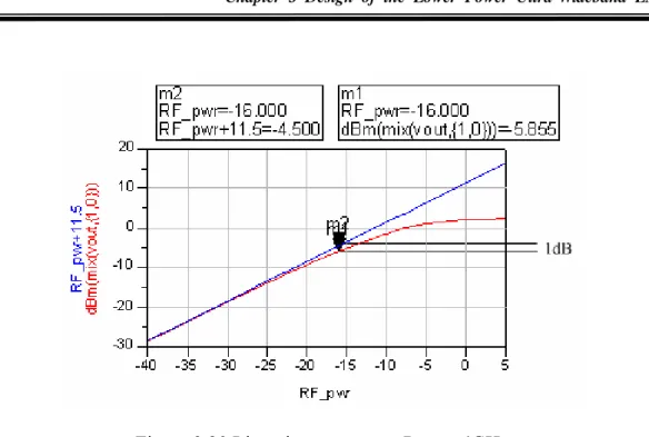
P1dB=P1dB(dBm)=G1dB(dB)+IP1dB(RF_pwr)(dBm) =12.44+(-19)=-6.56dBm
Simulation results of P1dB=-7.8dBm.
Figure 3.25 Linearity parameters OIP3 at 6GHz Linearity parameters OIP3 can be explained by Figure 3.28. OIP3=Pout+1
2IMD=-8.682+ 1
Chapter 3 Design of the Lower Power Ultra-Wideband LNA
Figure 3.26 Linearity parameters P1dB at 7GHz
Linearity parameters P1dB can be explained by Figure 3.29.
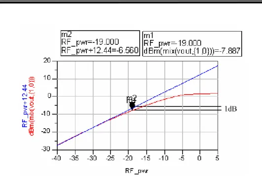
P1dB=P1dB(dBm)=G1dB(dB)+IP1dB(RF_pwr)(dBm) =12.44+(-20)=-7.56dBm
Simulation results of P1dB=-8.8dBm.
Figure 3.27 Linearity parameters OIP3 at 7GHz Linearity parameters OIP3 can be explained by Figure 3.30. OIP3=Pout+1
2IMD=-8.85+ 1
Chapter 3 Design of the Lower Power Ultra-Wideband LNA
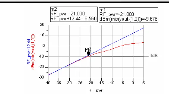
Figure 3.28 Linearity parameters P1dB at 8GHz
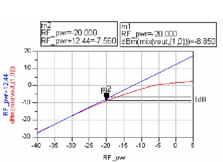
Linearity parameters P1dB can be explained by Figure 3.31.
P1dB=P1dB(dBm)=G1dB(dB)+IP1dB(RF_pwr)(dBm) =12.44+(-21)=-8.56dBm
Simulation results of P1dB=-9.84dBm.
Figure 3.29 Linearity parameters OIP3 at 8GHz Linearity parameters OIP3 can be explained by Figure 3.32. OIP3=Pout+1
2IMD=-9.051+ 1
Chapter 3 Design of the Lower Power Ultra-Wideband LNA
Figure 3.30 Linearity parameters P1dB at 9GHz
Linearity parameters P1dB can be explained by Figure 3.33.
P1dB=P1dB(dBm)=G1dB(dB)+IP1dB(RF_pwr)(dBm) =12.44+(-21)=-8.56dBm
Simulation results of P1dB=-9.67dBm.
Figure 3.31 Linearity parameters OIP3 at 9GHz Linearity parameters OIP3 can be explained by Figure 3.34. OIP3=Pout+1
2IMD=-8.92+ 1
Chapter 3 Design of the Lower Power Ultra-Wideband LNA
Figure 3.32 Linearity parameters P1dB at 10.6GHz
Linearity parameters P1dB can be explained by Figure 3.35.
P1dB=P1dB(dBm)=G1dB(dB)+IP1dB(RF_pwr)(dBm) =10+(-14)=-4dBm
Simulation results of P1dB=-5.7dBm.
Figure 3.33 Linearity parameters OIP3 at 10.6GHz Linearity parameters OIP3 can be explained by Figure 3.36. OIP3=Pout+1
2IMD=-10.324+ 1
Chapter 4 Design of the Low Voltage Ultra-Wideband LNA
Chapter 4 Design of the Low Voltage Ultra-Wideband
Low Noise Amplifier
4.1 Introduction
A very low-voltage ultra-wideband (UWB) low-noise amplifier (LNA) is achieved by reducing transistor’s threshold voltage using an external bias to the transistor body node. To achieve ultra-wideband input impedance matching, a novel design is proposed for the LNA by adding a feedback resistor Rf to a conventional LNA cascode
architecture. Based on TSMC 0.18μm 1P6M process, the numerical result shows that the LNA has 11.8~14.0dB gain from 6 GHz to 10.0 GHz with input matching S11<-13.7dB and 2.81dB noise figure in 7.0GHz. It only dissipates 2.8 mW with a small power supply of 0.75V.
4.2 Proposed LNA with feedback resistor architecture
The proposed ultra-wideband Low Noise Amplifier architecture is shown in Figure 4.1,which is different from the conventional narrowband cascode Low Noise Amplifier
Chapter 4 Design of the Low Voltage Ultra-Wideband LNA
architecture [8], [17] by adding a feedback circuit. In Figure 4.2, Rf is added as a
feedback element to the conventional cascode narrowband and Low Noise Amplifier and Ld, and Rd are used as peaking loads at the output [1], [10]. The capacitor Cf and C1
are used for ac coupling capacitors. The Sources-follower buffer M3 is designed for
output matching, with the bias current at 5mA.
Figure 4.1 Conventional narrowband cascode LNA
Figure 4.2 The proposed ultra-wideband LNA, which is resistor feedback configuration
Chapter 4 Design of the Low Voltage Ultra-Wideband LNA
4.2.1 Resistive shunt feedback technique
The resistor feedback configuration is the most common method of negative feedback technique. First, determination of feedback resistance value Rf is important. In
the proposed Low Noise Amplifier, the values of feedback resistors Rf (300-2000Ω) are
employed to produce the wideband input impedance matching, without affecting the Noise Figure (NF) significantly. Due to the Noise Figure of the feedback amplifier cannot be optimized without sacrificing other important performance such as gain, gain flatness, input/output return loss.
Table 4.1 represents the minimum Noise Figure (NFmin), gain flatness, and input
return loss (S11) of the feedback amplifier by different resistance values. In order to achieve a gain flatness of between 6.0-10.6 GHz, return loss S11<-10dB of 6.0GHz-10.6 GHz, and the noise figure of less than 2.5dB, the feedback resistance was chosen to between 800Ω and 1000Ω. Therefore, the Low Noise Amplifier can be tuned to achieve proper resistance value Rf for a wideband frequency range.
Table 4.1 Effect on feedback resistance
Feedback Rf NFmin Gain Flatness (-3dB range) Return Loss S11< -10dB
300 Ω 2.9 dB 6.9-11.3 GHz 2.0-8.7 GHz 500 Ω 2.55 dB 5.5-10.6 GHz 3.8-10.2 GHz 800 Ω 2.36 dB 4.4-10.4 GHz 5.0-10.6 GHz 1000 Ω 2.3 dB 4.0-10.4 GHz 5.4-10.8 GHz 2000 Ω 2.26 dB 3.1-10.4 GHz 6.0-10.7 GHz
From the smith chart in Figure 4.3, shows the simulated S11 of the proposed Ultra wideband Low Noise Amplifier with feedback resistor Rf=1000Ω and compares that of