高速與低功率邏輯應用之砷化銦鋁/砷化銦鎵變異結構高電子移動率電晶體之研究
129
0
0
全文
(2) 高速與低功率邏輯應用之砷化銦鋁/砷化銦鎵變異結構高電 子移動率電晶體之研究. The Study of InAlAs/InxGa1-xAs Metamorphic High Electron Mobility Transistors for High Speed and Low Power Logic Applications. 研 究 生:郭 建 億. Student: Chien-I Kuo. 指導教授:張. Advisor: Dr. Edward Yi Chang. 翼 博士. 國立交通大學 材料科學與工程研究所 博士論文 A Dissertation Submitted to Department of Materials Science and Engineering College of Engineering National Chiao Tung University In Partial Fulfill of the Requirements For the Degree of Doctor of Philosophy in Engineering 2008 Hsinchu, Taiwan, Republic of China. 中華民國九十七年七月.
(3) 高速與低功率邏輯應用之砷化銦鋁/砷化銦鎵變異結構高電子移動率 電晶體之研究. 研究生:郭 建 億. 指導教授:張 翼 博士. 國立交通大學材料科學與工程研究所. 摘要. 本研究成功製作高頻與低功率邏輯應用之高效能砷化銦鋁/砷化銦鎵變異 結構高電子移動率電晶體 (Metamorphic High Electron Mobility Transistors, MHEMTs),並且對此元件做了深入的分析與探討。為了增進此變異結構高電子 移動率電晶體之特性,在改善元件磊晶結構的同時,也搭配了奈米級閘極線寬與 白金閘極掘入 (Pt-buried gate) 的技術。另外,也對未來 N 型金氧半場效電晶體 極具潛力的三五半導體通道材料其表面處理方式做了詳細的探討。 在論文中,研發出以白金閘極掘入的技術應用在以砷化銦 (InAs) 為通道 的 HEMT 元件上。利用此方式有許多的優點,白金的功函數較傳統以鈦金屬閘 極高,在掘入蕭基特層後,不但可以縮短電極與通道間距離,藉以抑制短通道效 應外,還可以降低漏電流與源極阻抗等等,進而改善微波與邏輯特性。用此方法 製作的 HEMT 元件具有 1418 mA/mm 的汲極-源極電流以及 1600mS/mm 的高轉 導值。此元件與未有閘極掘入元件相較下,截止頻率(fT)由原本的 390 GHz 提升 到 494 GHz,最大震盪頻率(fmax)也由原本的 360 GHz 提升到 390 GHz。在雜訊指 數方面,在 17 GHz 頻率下為 0.82 dB 且相對應的增益(associated gain)為 14 dB, 其量測的汲極偏壓為 0.3V 而直流消耗功率僅 1.14 mW,顯現此元件極有潛力作 i.
(4) 為低電壓的小訊號放大器,此外由於閘極掘入後,閘極漏電與閘極-源極電容值 皆變小,使得在元件閘極延遲時間上達到 0.78 picosecond 且其開關電流比值依舊 維持在三個數量級。 另外,更進一步的縮小源極與汲極間距,期使元件的邏輯特性更加優異, 並且成功的應用在 HEMT 元件製作上,同時也分析了這種窄能隙半導體其撞擊 離子化的現象並與先進的矽半導體元件及砷化銻(InSb)元件做了詳細的比較與邏 輯特性分析。此砷化銦為主通道,銦含量高達 70%的砷化銦鎵為次通道的元件, 其發生撞擊離子化偏壓點約為 0.8 V 左右。在邏輯特性方面,此元件的汲極引致 能障下降為 200mV/V,次臨界擺幅約 115 mV/dec,在偏壓 0.5 V 時展現了 0.54 picosecond 的閘極延遲,但由於其通道為窄能隙半導體,關閉態的漏電流較大, 起因於蕭基特閘極漏電與能帶能帶間的穿遂電流,但相較於砷化銻通道元件佳。 此外,與先進的矽奈米元件相比,砷化銦通道 HEMTs 展現了優異的閘極延遲與 3.1 倍高的 fT 於相同直流消耗功率上等特性。因此,III-V 高速元件將會是在後矽 半導體世代扮演重要的角色。 另外,論文中也探討了以 10 奈米厚的二氧化鋯高介電常數材料製作的假 晶砷化銦鎵(In0.53Ga0.47As)金氧半電容結構。在成長介電薄膜時砷化銦鎵的表面 也做了以硫化銨與稀釋鹽酸處理。比較兩者之後發現,經過硫化處理與 350 度退 火後的電容結構具有良好的電容-電性特性(強反轉現象),高崩潰電壓,與低漏電 等,可見其具有較低的介面缺陷或是較少的不完美鍵結因而減低了費米釘札 (Fermi-level pinning)。由材料分析得知,在高解析度的穿透式電子顯微鏡下可看 到約 20Å 的薄膜介於半導體與介電薄膜中,進一步透過二次離子質譜儀分析, 此薄膜為硫元素。因此證明了以硫化銨處理後其可以保護三五半導體表面發生原 生氧化層導致元件特性變差。. ii.
(5) The Study of InAlAs/InxGa1-xAs Metamorphic High Electron Mobility Transistors for High Speed and Low Power Logic Applications. Student: Chien-I Kuo. Advisor: Dr. Edward Yi Chang. Department of Materials Science and Engineering National Chiao Tung University. Abstract. High performance eighty nanometer gate length InAlAs/InxGa1-xAs metamorphic high electron mobility transistors (MHEMTs) have been fabricated successfully and characterized for high frequency and low-power logic applications. The performance of the MHEMTs was improved by optimizing the device structure, using the Pt-buried gate techniques and shrinking the source-drain spacing. In addition, the surface pre-treatments of III-V channel material before high-k deposition for future III-V nMOSFET were also studied. In this dissertation, the fabrication of 80 nm InAs channel MHEMTs using Pt gate-sinking was developed. There are several advantages to improve RF and logic performance with gate-sinking process such as high metal work function, suppression the short channel effect, the reduction of the gate leakage current and decrease of the source resistance. The fabricated InAs MHEMT using this technique shows a drain-source current of 1418 mA/mm and transconductance of 1600 mS/mm. The cutoff frequency fT and maximum oscillation frequency fmax of the MHEMT with Pt-buried gate are 494 GHz and 390 GHz as compared with that of 390 GHz and 360 iii.
(6) GHz for device without gate sinking, respectively. The noise figure of the InAs MHEMT was 0.82dB and the associated gain was 14 dB at 17GHz under the bias condition of VDS = 0.3 V, indicating great potential for low-power LNA application. Because of the reduction of gate leakage current and gate-to-source capacitance, the intrinsic gate delay of the device is 0.78 picosecond, while maintaining an ION/IOFF ratio above 103. In addition, to promote the logic performance of InAs HEMT, device with small source-drain spacing were fabricated for high speed and low-voltage digital applications. Care must be taken while biasing device with such narrow energy bandgap when the impact ionization occurred in order to avoid the degradation of devices. Performance degradations were observed on the DC and RF characteristics due to impact ionization when the drain bias VDS > 0.8 V. For logic parameters, a drain-induced barrier lowering of 200 mV/V, a subthreshold slope of 115 mV/dec and a very low gate delay of 0.54 ps were obtained. Besides, InAs HEMTs exhibit excellent logic performances such as gate delay and 3.1 times higher fT at the same DC power dissipation when benchmarking advanced Si MOSFETs. Therefore, III-V high speed device has great potential to play an important role in Post-Si era. In addition, the electrical properties of the metamorphic In0.53Ga0.47As metal-oxide-semiconductor capacitors with a 100-Å-thick ZrO2 layer as high-k dielectrics were investigated. The In0.53Ga0.47As surface was pretreated by either sulfur passivation or HCl cleaning before the ZrO2 deposition. Owing to the lower interface-state density or Fermi-level unpinning after sulfidation, the sulfur-passivated capacitor exhibited better accumulation capacitance and strong inversion at capacitance-voltage measurement than the HCl-cleaned capacitor after post deposition annealing at 350 oC. On the basis of material analyses including High Resolution TEM and Secondary Ion Mass Spectrometer, the capacitors that subjected to sulfur iv.
(7) treatment were found to contain a thin sulfur layer on the interface, which protects the surface from oxidation and prevents performance degradation.. v.
(8) 誌. 謝. 漫長的博士班生涯隨著論文的結束即將劃上完美的句號,首先最要感謝我 的博士班指導教授 張翼博士。這些年裡,在老師的開明作風與悉心指導下,使 我在獨立思考與解決問題能力上成長許多,此外老師提供了相當充足的儀器資 源,讓我能全程參與美國英代爾半導體公司的尖端研究計畫,並且有機會前往日 本東京工業大學(TITech)學習先進電子束微影技術,拓展研究的視野與世界觀, 並學習日本人嚴謹的研究精神,同時老師也給予我許多機會參加國際會議,吸取 國外半導體的新知,這些難能可貴的經歷與學習經驗,讓我受用無窮。 在這裡同時要特別感謝元智大學許恆通博士,他的耐心指導與每每在深夜 裡的討論、實驗分析,使我減少許多摸索的時間也一起渡過許多英代爾 quarter review 準備報告的日子。此外也要謝謝在 TITech 的日子裡,Yasuyuki Miyamoto 教授,Takeshi Yamaguchi 先生以及 Susumu Kenmochi 先生,對我在日本東京做 研究時的關心照顧以及實驗上的協助。感謝國家奈米元件實驗室(NDL)許多的工 程師(邱佳松、鄧裕民、陳文林與廖國祥先生等)及交大奈米中心,同時提供優 良的儀器設備與環境,使實驗能夠更加順利進行。 另外我也要感謝 CSD Lab.的許多伙伴,謝炎璋博士、連亦中博士、褚立新 博士,陳俊淇博士等學長的鼓勵,還有陪伴我走過五年同窗生活的黃瑞乾同學、 張家源同學、呂宗育同學,林龔樑同學與吳雲驥同學,還有許多可愛的學弟妹, 張家達、許立翰、李芳銘、唐士軒、王景德、曾文仲、蕭佑霖、黃偉進、曾育玲、 吳建瑩、陳鈺霖、蘇詠萱等,在實驗與生活上的幫忙使我不致感到孤立無援,以 及詹前璋先生在儀器設備及廠務方面的幫忙。也要謝謝江韵涵、陳善理、黃碧玉、 余蕙馨及鍾盈怡等諸位美麗的小姐在行政上的協助幫忙。 謝謝大學同學,柯利昇、邱介宏、張耀仁與許智明等伙伴與友達光電的王 賢軍先生、力晶半導體的林嘉柏先生及茂德科技李偉強博士的相助與相挺,讓我. vi.
(9) 在無趣博士班日子裡過得充實。 最後,我要特別感謝在我的背後精神上支持與鼓勵的親人等,郭芳永先生、 房春生先生、蘇真女士、楊春霞女士,以及哥哥與大嫂,感謝您們的關心、支持、 包容與鼓勵,使我無後顧之憂,能夠專心順利完成學業,當然還有最重要的貼心 女友妤真,謝謝她一路相伴,默默的支持,一同度過許多低潮時光,不如意日子, 畢業是人生另一階段的開始,也是換我好好照顧妳的日子。願這份榮耀與您們分 享。. vii.
(10) Contents. Abstract (in Chinese)………………………………………………….…i Abstract (in English)…………………………………………………iii Acknowledge (in Chinese)……………………………………………vi Contents……………………………………………………………….viii Table Captions………………………………………………….…….xi Figure Captions…………………………………………………….…xii. Chapter 1 Introduction…………………………………………………1 1.1 General Background and Motivation………….………………………………..1 1.2 Overview of High Electron Mobility Transistors (HEMTs)……..……………..2 1.3 Logic Suitability of HEMTs for Beyond-CMOS Applications……....………....3 1.4 Outline of the Dissertation……...……………………………………………....4. Chapter 2 Fabrication of InxGa1-xAs-Channel Metamorphic High Electron Mobility Transistors……………………………...………….14 2.1 Device structure…………………………………..….………….……………..14 2.2 Device Fabrication……….…………………………………………......……14 2.2.1 Mesa isolation…………………………………………………………….15 2.2.2 Ohmic contact Formation……………………….………………………...15 2.2.3 Fabrication of T-shaped gate process by E-Beam lithography……….16 2.2.4 Gate recess………………………………………………………………...16 2.2.5 Device passivation…………………………..…….………………………17 2.2.6 Airbridge formation….………….……………….……………………..18. viii.
(11) Chapter 3 DC and RF Measurements of InxGa1-xAs Metamorphic High Electron Mobility Transistors……………………………..…....26 3.1 Device Characterization………………………………………………………..26 3.2 DC characteristics……………………………………………………….……...27 3.3 Breakdown characteristics……………………………………………………...29 3.4 Scattering parameters………………………………...…………………...….30 3.5 Current gain cutoff frequency fT and Maximum frequency of oscillation fmax……………………………..……………………………………………..……………….31 3.6 Device modelling technique…………..…………………....…………………...32 3.7 Noise figure………..………………………………..……………...…………...33. Chapter 4 RF and Logic Performance Improvement of In0.7Ga0.3As /InAs/In0.7Ga0.3As Composite Channel HEMT Using Gate Sinking Technology…..……………………………….………………………....41 4.1 Introduction…………………………………………………………………..41 4.2 Experimental…………………………………………………………………...42 4.3 Results and Discussion…………………...…………………………………….43 4.4 Conclusion………………...……………………………………………………46. Chapter 5 InAs-Channel Based Quantum Well Transistors for High-Speed and Low-Voltage Digital Applications………………….60 5.1 Introduction…………………………...………………………………………..60 5.2 Experimental……………………………………………………………...……61 5.3 Results and Discussion………………...……………………………………….62 5.4 Conclusion………………………………………...……………………………66. ix.
(12) Chapter 6 Metamorphic In0.53Ga0.47As Metal-Oxide-Semiconductor Structure on a GaAs Substrate with ZrO2 High-k Dielectrics.........84 6.1 Introduction………………………..………………………………..………….84 6.2 Experimental…………………………………………………………………85 6.3 Results and Discussion………………..………………………….………….....86 6.4 Conclusion……………………………….…………………………………..88. Chapter 7 Conclusion……………………..…………………………...97. Reference…………………………………………………………….99. Vita (in Chinese). Publication List. x.
(13) Table Captions. Chapter 1 Table 1.1 The bulk electron and hole mobility, the electron and hole effective mass, and the bandgap and the permittivity of Si, Ge, and main III-V semiconductor……...7 Table 1.2 Best performance of InP HEMTs and GaAs-based MHEMTs published in recent years……………………………………………………………………………8. Chapter 2 Table 2.1 The detailed expitaxial structures of the devices with different Indium content in InxGa1-xAs channel from 52%, 70% to 100%.............................................19. Chapter 4 Table 4.1 Summary of the HEMT device parameters with and without gate sinking..59. xi.
(14) Figure Captions. Chapter 1 Fig. 1.1 The trend of transistor technology……………………………………………9 Fig. 1.2 Conventional HEMT structure………………………………………………10 Fig. 1.3 Band Diagram of InAlAs/InGaAs MHEMTs……………………………….11 Fig. 1.4 Electrical figures of merit of a transistor as a switch………………………..12 Fig. 1.5 Evaluation methodology for the logic performance of HEMTs…………….13. Chapter 2 Fig. 2.1 Optimization of RTA Temperature for Ohmic Contact……………………...20 Fig. 2.2 TLM pattern…………………………………………………………………21 Fig. 2.3 The illustration of utilizing TLM to measure ohmic contact resistance….…21 Fig. 2.4 T-shaped gate process flow………………………………………………….22 Fig. 2.5 The dose dependence of the gate foot size after development……………....23 Fig. 2.6 The 40 nm T-shaped gate resist profile……………………………………...24 Fig. 2.7 SEM image of the finished airbridge………………………………………..25. Chapter 3 Fig. 3.1 Band diagrams at three different locations along the channel of a HEMT….35 Fig. 3.2 Actual characteristics and those predicted by Eq. (3-3)……………………..36 Fig. 3.3 Detailed layout of the device, the pads connecting the gate and drain are about 50×100um2…………………………………………………………...37 Fig. 3.4 The block diagram with determined parasitic elements for the overall device structure……………………………………………………………………..38 xii.
(15) Fig. 3.5 Functional blocks of the equivalent circuit model, divided according the scalability with device size………………………………………………...39 Fig. 3.6 Analyzed electric field plot of the 2x50um device at 10 GHz. (a) with the source buses of the device (b) without the source buses of the device……..40. Chapter 4 Fig. 4.1 The schematic view of the device structure and the insert SEM image is the 80-nm T-shaped gate after recess before silicon nitride passivation……….48 Fig. 4.2 Drain-source current versus drain-source voltage curve for device with gate sinking……………………………………………………………………...49 Fig. 4.3 Drain-source current versus drain-source voltage curve for device without gate sinking………………………………………………………………...50 Fig. 4.4 Two terminal gate-to-drain breakdown characteristics of device with/without gate sinking………………………………………………………………...51 Fig. 4.5 Transconductance versus gate-source voltage before and after gate sinking at 250oC for 3 min……………………………………………………………52 Fig. 4.6 Frequency dependence of the current gain H21, the power gain MAG/MSG, and the unilateral gain U of the InAs/In0.7Ga0.3As composite channel HEMTs. The frequency range was from 5 to 80 GHz, and the device was biased at Vds = 0.8V and Vgs = -0.5V……………………………………………………..53 Fig. 4.7 Typical current gain H21, MAG/MSG, and unilateral gain U as a function of frequency of the 0.08 × 100 µm2 HEMTs before gate sinking……………...54 Fig. 4.8 Measured S11 of devices with and without gate sinking under the same bias condition. Note that this bias condition gives the smallest intrinsic gate delay for the devices………………………………………………………...55 Fig. 4.9 Measured noise performance of the device at drain voltage VDS = 0.1V (a) xiii.
(16) device with gate sinking, Ids = 0.25 mA/mm (b) device without gate sinking, Ids=0.34 mA/mm…………………………………….……………………...56 Fig. 4.10 Measured noise performance of the device at drain voltage VDS = 0.3V (a) device with gate sinking, Ids = 3.80 mA/mm (b) device without gate sinking, Ids = 2.52 mA/mm…………………………………………………………...57 Fig. 4.11 The calculated intrinsic gate delay as a function of ION/IOFF ratio with various choices of the threshold voltage for device with/without sink……..58. Chapter 5 Fig. 5.1 Epitaxial layer structure of the InAs/In0.7Ga0.3As HEMTs………………….67 Fig. 5.2 Drain-source current versus drain-source voltage curve................................68 Fig. 5.3 Current-voltage characteristics at different VDS of 0.08 × 40 µm2 QWFETs...........................................................................................................69 Fig. 5.4 Current-voltage characteristics of In0.52Ga0.48As QWFETs…………………70 Fig. 5.5 Current-voltage characteristics of In0.7Ga0.3As QWFETs…………………...71 Fig. 5.6 Cutoff frequency vs. Ids and VDS of InAs QWFETs………………………...72 Fig. 5.7 Frequency dependence of the current gain H21, and the power gain MAG/MSG of the InAs/In0.7Ga0.3As composite channel QWFETs. The frequency range was from 5 to 80 GHz, and the device was biased at VDS = 0.5 V and Vgs = - 0.45 V…………………………………………………...73 Fig. 5.8 InAs/In0.7Ga0.3As Channel HEMTs (a) Plot of H21 measured at 80 GHz versus drain-source voltage of 0.08 × 100 µm2 (b) Gate current IG plotted as a function of VG at different Vds from 0 V to 0.9 V…………………………..74 Fig. 5.9 The sub-threshold characteristics of the device with InAs channel at the VDS of 0.05 and 0.5V……………………………………………………………75. xiv.
(17) Fig. 5.10 The sub-threshold characteristics of the device with In0.7Ga0.3As channel at the VDS of 0.05 and 0.5V……………………………………………………………..76 Fig. 5.11 The methodology for the evaluation of the logic performance of novel devices with non-optimized VT. Different definitions of VT result in a new set of logic parameters of C’V’/I’………………………………………………………………...77 Fig. 5.12 Gate delay as a function of the selected threshold voltage………………...78 Fig. 5.13 ION/IOFF ratio as function of various VT at the drain voltage 0.5 V………...79 Fig. 5.14 Comparison between gate delay and ION/IOFF of 80 nm InAs QWFETs, 200 nm InSb QWFETs and 40 nm Si MOSFETs………………………………..80 Fig. 5.15 Cutoff frequency of InAs QWFETs and 80 nm Si MOSFETs as a function of the power dissipation……………………….……………………………….81 Fig. 5.16 Gate delay of InAs, InSb QWFETs and Si NMOSFETs as a function of gate length………………………………………………………………………82 Fig. 5.17 I-V characteristics of MIS QWFETs and Schottky metal gate QWFETs….83. Chapter 6 Fig. 6.1 Cross-sectional view of MOS capacitor structure…………………………..90 Fig. 6.2 (a) AFM image of surface of HCl-cleaned (Treatment A) MOS after ZrO2 deposition, RMS = 0.841 nm. (b) AFM image of surface of sulfur-passivated (Treatment B) MOS after ZrO2 deposition, RMS = 0.730 nm……………..91 Fig. 6.3 High-resolution TEM cross-sectional images of ZrO2/ In0.53Ga0.47As gate dielectric stack: (a) HCl-cleaned sample, (b) (NH4)2Sx-treated sample…….92 Fig. 6.4 SIMS depth profiles of S, Zr, In, Ga, and As elements and 34S density of MOS capacitor subjected to Surface Treatment B………………………………...93 Fig. 6.5 High-frequency C-V characteristics of In0.53Ga0.47As MOS capacitors with xv.
(18) surface Treatment A after different PDA temperatures……………………..94 Fig. 6.6 High-frequency C-V characteristics of In0.53Ga0.47As MOS capacitors with surface Treatment B after different PDA temperatures……..……………..95 Fig. 6.7 Comparison of leakage current of MOS structure after different surface treatments. …………………………………………………………...……96. xvi.
(19) Chapter 1. Introduction. 1.1 General Background and Motivation. With the rapid progress of wireless communication industries, the applications have moved from the microwave toward millimeter wave frequency range. Consequently, the required performance specifications for the key components are getting more and more rigid. III-V based compound semiconductor devices such as GaAs pseudomorphic high electron mobility transistors (PHEMTs), metamorphic HEMTs. (MHEMTs),. conventional. lattice-matched. or. pseudomorphic. InAlAs/InGaAs/InP HEMTs (InP HEMTs) with high indium mole fraction channel, have shown superior performance as compared to the Si devices in high-frequency and high-speed applications. Many efforts have been made to improve the high-frequency performance of the III-V devices by means of refined heterjunction structure, and sub-nanometer gate length. Nanometer-T-shaped gate is generally used for the HEMTs to maximize the device performance. On the other hand, the size scaling of CMOS has followed the famous Moore’s law for over 30 years. In the current 65nm technology node, the gate length of a Si MOSFET is about 30 nm and such dimension is expected to reach about 10 nm by 2011, which is believed to be the ultimate limit for CMOS scaling. The trend of transistor technology is shown in Fig. 1.1 and several novel devices technology candidates that are often mentioned to replace Si CMOS including carbon nanotube 1.
(20) (CNT) transistors, semiconductor nanowires and spintronics [1-1]. While the majority of the above mentioned technologies are still in the prototyping stage, recent development in device technology of III-V FETs, especially the heterostructure HEMT devices has shown great potential to be the next generation high-speed logic device technology due to its maturity in device fabrication technologies and excellent RF performance. Attention has recently been paid to III-V channels as a promising candidate of high performance n-MOSFETs beyond strained-Si devices [1-2]. This is because III-V compound semiconductors have ~ 50-100 x higher electron mobility than Si and III-V nMOSFET can exhibit very attractive and tangible worth. Table 1.1 lists the properties of some channel materials [1-3]. It is confirmed that III-V materials can play an important role in future high-speed, and low power CMOS logic transistors in the Post-Si era. However, the key challenge for III-V-based MOSFET is the lack of high-quality, thermodynamically stable insulators that passivate the interface states and prevent Fermi level pinning at III-V-gate dielectric interface [1-4 - 1-6]. Many research groups have reported the necessary of special treatment on the III-V substrate surface prior to depositing the gate dielectrics such as interface passivation layer or plasma nitridation [1-7,1-8]. In this study, HEMTs with several device structures were fabricated successfully and evaluated characteristics of these devices for high frequency, high speed and logic applications. In addition, fabrication of high-k material on III-V compound semiconductor capacitors using different surface treatments was also studied.. 1.2 Overview of High Electron Mobility Transistor. High electron mobility transistor (HEMT) or called Quantum-well field-effect 2.
(21) transistor (QWFET) is one of the most mature III-V semiconductor transistors which rely on the use of heterojunction for its operation. The first demonstration of the HEMT was made by Fujitsu Lab. in 1980 [1-9]. Fig. 1.2 represents a cross-sectional view of a conventional HEMT structure. The epitaxial layers of the HEMT structure are designed to form two-dimension electron gas (2-DEG) in the channel layer with an un-doped spacer in the wide band gap material and narrow band gap material to separate the ionized donors from the channel. The detailed description of energy band diagram of InAlAs/InGaAs Metamorphic HEMTs is shown in Fig. 1.3 [1-10]. As a result, HEMTs have superior carrier transport properties due to the band-gap engineering design. For the past 5 years, GaAs-based MHEMTs and InP-based HEMTs with remarkable device performance for high frequency applications have been published and these results are listed in Table 1.2. As seen from this table, high indium content channel material HEMTs with nanometer gate length is the main way to enhance the device performance.. 1.3 Logic Suitability of HEMTs for Beyond-CMOS Applications. Lately, III-V technologies have attracted again for logic circuit when CMOS roadmap comes to the end. The main reason is the manufacturing technology for III-V devices is relatively mature compared to other novel devices such as carbon-nanotube transistors and semiconductor nanowires. In digital application, a transistor operates as a switch and is different form in microwave or millimeter wave application. Fig. 1.4 shows the electrical figures of merit of a transistor as a switch [1-11]. As seen from the figure, figures of merit relevant to logic application, for example drain-induced barrier lowering (DIBL), subthreshold slope (S), on-state and off-state 3.
(22) current ratio, and the delay time (CV/I), these are important parameters for these devices to be used for future digital applications. In this study, we have applied a methodology that was recently proposed to analyze new devices which often feature nonoptimized values of VT [1-12]. The evaluation methodology is shown in Fig. 1.5. First, we select gate-to-source voltage at 1mA/mm of drain-source current as the threshold voltage. Then we selected ION as 2/3 VCC swing above the threshold voltage, and IOFF as 1/3 VCC swing below the threshold voltage. Based on this definition, we extracted and compared the device’s logic parameters, such as subthreshold slope, DIBL and ION/IOFF ratio for the InxGa1-xAs HEMTs developed in this study.. 1.4 Outline of this dissertation. This dissertation covers the study of RF and logic evaluation of InxGa1-xAs channel HEMTs and the metamorphic In0.53Ga0.47As MOS capacitors with zirconium dioxide (ZrO2) high-k dielectrics. It is divided into 7 chapters. In chapters 2, the details of the fabrication process of the InxGa1-xAs HEMTs are introduced, including the mesa isolation, ohmic contact formation, T-shaped gate process, gate recess, SiNx passivation and airbridge formation. In chapter 3, the DC and RF characterizations of the device are described. In. chapter. 4,. the. results. of. RF. and. logic. evaluation. of. the. In0.7Ga0.3As/InAs/In0.7Ga0.3As channel HEMTs with Pt-buried gate are given. The current gain cutoff frequency of the 80 nm gate-length device increased from 390 GHz to 494 GHz and the gate delay time decreased from 0.83 psec to 0.78 psec after the gate sinking process. The improvements of the device characteristics are due to the reduction of gate-to-source capacitance (Cgs) and the source resistance (Rs) after 4.
(23) gate sinking. In addition, for ultra-low power low-noise amplifier application, the InAs channel device demonstrates excellent dc power consumption with higher gain compared with other GaAs- or InP –based HEMTs to date. In chapter 5, the figures of merit relevant to logic, such as gate delay, ION/IOFF, DIBL, and S of the InAs-channel HEMTs with 2 µm source-drain spacing for low-voltage digital applications, are studied. Besides, the bias conditions for the narrow energy bandgap electron devices before occurrence of impact ionization are studied. In chapter 6, the electrical properties of metamorphic In0.53Ga0.47As metal-oxide-semiconductor capacitors with a 100-Å-thick ZrO2 as high-k dielectrics are studied. The In0.53Ga0.47As surface was pretreated by either sulfur passivation or HCl cleaning before the ZrO2 deposition. Owing to the lower interface-state density after sulfidation, the sulfur-passivated capacitor exhibited better accumulation capacitance and strong inversion at capacitance-voltage measurement than the HCl-cleaned capacitor after post deposition annealing at 350oC. On the basis of material analyses including high resolution TEM and SIMS, the capacitors that subjected to underwent sulfur treatment were found to contain a thin sulfur layer on the interface, which protects their surface from air exposure and prevents performance degradation. Finally, chapter 7 is the conclusion of the dissertation. The RF and Logic performances of the InAs channel HEMTs was improved by using Pt-buried gate due to the reduction of gate-to-channel distance, small Cgs and the small Rs. The InAs HEMTs showed excellent DC and RF performances after gate sinking, indicating great potential for this device for low voltage high-speed digital applications. In addition, the metamorphic In0.53Ga0.47As MOS capacitors with ZrO2 exhibit better C-V characteristics and show reduced leakage current after sulfur pretreatment. 5.
(24) The removal of the defective bonding states and the enhanced barrier for the electron conduction due to the unpinning of Fermi level, are primarily responsible for the improvement of the electrical characteristics.. 6.
(25) Table 1.1 The bulk electron and hole mobility, the electron and hole effective mass, and the bandgap and the permittivity of Si, Ge, and main III-V semiconductor.. 7.
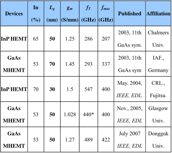
(26) In. Lg. gm. fT. fmax. Devices. Published Affiliation (%). (nm) (S/mm) (GHz) (GHz) 2003, 11th. Chalmers. GaAs sym.. Univ.. 2003, 11th. IAF.,. GaAs sym. Germany. May. 2004,. CRL.,. IEEE, EDL.. Fujitsu.. Nov., 2005,. Glasgow. MHEMT. IEEE, EDL. Univ.. GaAs. July 2007. Dongguk. IEEE, EDL. Univ.. InP HEMT. 65. 50. 1.25. 286. 207. GaAs 53. 70. 1.45. 293. 337. MHEMT. InP HEMT. 70. 30. 1.5. 547. 400. GaAs 53. 53. 50. 50. 1.028. 1.27. 440*. 489. MHEMT. 400. 422. Table 1.2 Best performance of InP HEMTs and GaAs-based MHEMTs published in recent years.. 8.
(27) Fig. 1.1 The trend of transistor technology. 9.
(28) Fig. 1.2 Conventional HEMT structure.. 10.
(29) n-InAlAs. i-InGaAs. n-InAlAs i-InGaAs. Fig. 1.3 Band Diagram of InAlAs/InGaAs MHEMTs. 11.
(30) Fig. 1.4 Electrical figures of merit of a transistor as a switch. 12.
(31) Fig. 1.5 Evaluation methodology for the logic performance of HEMTs. 13.
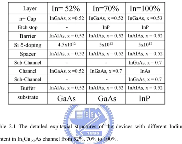
(32) Chapter 2. Fabrication of InxGa1-xAs-Channel Metamorphic High Electron Mobility Transistors. 2.1 Device structure. The epitaxial layers of the InxGa1-xAs-channel metamorphic HEMT with InxAl1-xAs grading buffer layer were grown on GaAs substrate or InP substrate by molecular beam epitaxy (MBE). Using metamorphic buffer layer provides the ability to accommodate the lattice mismatch between InxGa1-xAs channel and GaAs substrate. Therefore, the high indium content in the InxGa1-xAs channel can be achieved in spite of the large lattice mismatch between the active epilayers and the substrate. In this study, the detailed expitaxial structures of the devices with different Indium content in InxGa1-xAs channel from 52%, 70% to 100% are shown in Table. 2.1.. 2.2 Device fabrication. The fabrication process of HEMTs in this study includes several steps: 1.. Mesa isolation. 2.. Ohmic contact formation. 3.. Fabrication of T-shaped gate process by E-Beam lithography. 4.. Gate recess. 5.. Device passivation 14.
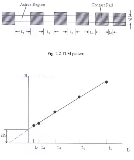
(33) 6.. Airbridage formation. 2.2.1 Mesa isolation. Device isolation is the first step of the whole HEMT fabrication process which was used to define the active region of the device on the wafer. For mesa isolations, the active areas were first masked by Shipley S1818 photo resist and then, the InGaAs/InAlAs layers was etched by a phosphoric based solution, following that, a hydrochloric acid based wet etch was used to etch the InP stopper layer [2-1]. According to the device structure, the mesa was etched to the buffer layer to provide good device isolation. Finally, the etching depth was measured by α-step after the photo-resist was stripped and the etched profile was checked by scanning electron microscopy.. 2.2.2 Ohmic contact formation. After wafer cleaning by using ACE and IPA, the negative photo resist and I-line aligner were used to define the Ohmic pattern and to form the undercut profile for the metal lift-off. HCl-based solution was used as the pre-metallization cleaning solution to remove the native oxide of the InGaAs surface before Ohmic metallization. Ohmic metals multilayer Au/Ge/Ni/Au, from the bottom to the top, was deposited in the appropriate composition by e-gun evaporation system. After lift-off process, source and drain Ohmic contacts were formed by annealing at adequate temperature for 25 sec in forming gas atmosphere. Fig. 2.1 shows the drain current as a function of RTA temperature at the drain bias of 0.5 V before gate recess. The best RTA temperature was 250 oC. Germanium atoms diffused into the heavily doped InGaAs during the 15.
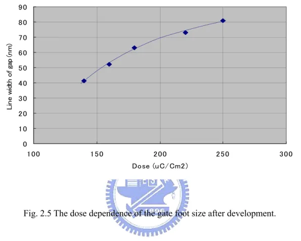
(34) thermal annealing process [2-2]. The specific contact resistance was checked by the transmission line method (TLM) in the process control pattern monitor (PCM). In this particular approach, a linear array of contacts is fabricated with various spacings between them as shown in Fig 2.2. The distances between TLM electrodes are 3 µm, 5 µm, 10 µm, 20 µm, and 36 µm, respectively in this study. The typical measured contact resistance was < 1 x 10⁻⁶ Ω-cm2 and the illustration of utilizing TLM to measure ohmic contact resistance was shown in Fig 2.3.. 2.2.3 Fabrication of T-shaped gate process by E-Beam lithography. Short gate length with low gate resistance is necessary for high frequency and high speed application. T-shaped gate structure was the most common approach for achieving low gate resistance and a small gate foot [2-3]. In this study, T-shaped gate was achieved by using a conventional multilayer resist (ZEP-520/PMGI/ZEP-520-12) with Electron Beam lithography. Fig. 2.4 summarizes the process flow of the fabrication of nanometer T-shaped gate. The first E-beam exposure for top two layers was used to only define the head (Tee-top) of the T-shaped gate by modulating the exposure doses. After that, the ZEP and PMGI development were executed by using xylene and MF622, respectively. Then, single center exposure with high dose was used to define the footprint of the bottom ZEP-520 layer. Fig. 2.5 shows the dose dependence of the gate foot size after development. The 40 nm T-shaped gate resist profile is illustrated in Fig. 2.6.. 2.2.4 Gate recess. The recess etching was performed using PH-adjusted solution of succinic (S.A.) 16.
(35) and H2O2 mixture for selective etching of the heavily doped InGaAs cap layer over InAlAs Schottky layer [2-4,2-5]. The concentration of the etchant should be adjusted to provide an etch rate that is sufficiently slow to allow good control over the recess process, thus enable the operation to approach the target current value, without over etching it. The etching selectivity of InGaAs cap layer over InAlAs Schottky layer was above 100. The target current after the gate recess is a critical parameter affecting the HEMT performance. In order to get the desired recess depth, the recess process was controlled by monitoring the ungated Ids. The method used to control the recess depth is to monitor the source-to-drain current during the etching process. For the low noise PHEMT, the saturation current and the slope of the linear region go down as the recess groove was etched deeper and deeper. The wet etchant usually leaves a thin oxide layer on the InAlAs. HCl-based solution was used to remove the surface oxide. After recess etching, Ti/Pt/Au gate metal was evaporated and lifted off using ZDMAC remover (ZEON Corporation) to form T-shaped gate.. 2.2.5 Device passivation. FETs are very susceptible to the surface condition, especially in the gate region. As the device scales down, the gate length and spaces of source-to-drain and gate-to-drain become smaller. In situation like this, the devices are very sensitive to the damages and contaminations such as chemicals, gases, and particles. The passivation layer protects the device from damage during process. The dielectric layer SiNx is a common choice for GaAs device passivation. In this study, STS PECVD system was used for depositing the silicon nitride film. The processing gases of the passivation PECVD were silane, ammonia, and nitrogen. The process condition was as following: process pressure: 900 mtorr, process temperature: 250°C and process 17.
(36) time: 10 minutes the silicon nitride film thickness was 600 Å. The reflection index was 2.0 as inspected by N&K anaylzer.. 2.2.6 Airbridge formation. Airbridge is built by metal with air between the metal interconnect and the wafer surface beneath. Airbridges are used extensively in GaAs analog devices and MMICs for interconnections. They may be used to interconnect sources of FETs, to cross over a lower level of metallization, or to connect the top plate of a MIM capacitor to adjacent metallization. The use of airbridge had several advantages including lowest dielectric constant of air, low parasitic capacitance, and the ability to carry substantial currents. The SEM image of the airbridge is shown in Fig. 2.7. 18.
(37) Table 2.1 The detailed expitaxial structures of the devices with different Indium content in InxGa1-xAs channel from 52%, 70% to 100%.. 19.
(38) 1700. Drain current (mA/mm). 1600. 0. Best RTA condition:250 C 25 sec in forming gas. 1500 1400 1300 1200 1100 1000 -50. 0. 50. 100. 150. 200. 250. 300. o. RTA temperature ( C). Fig. 2.1 Optimization of RTA Temperature for Ohmic Contact.. 20.
(39) Fig. 2.2 TLM pattern. Fig. 2.3 The illustration of utilizing TLM to measure ohmic contact resistance. 21.
(40) ZEP-520-12. ZEP-520-12. PMGI. PMGI. PMGI. ZEP-520 1:1. ZEP-520 1:1. ZEP-520 1:1. Substrate. Substrate. Substrate. Photoresist coating. Top part of T-shaped gate exposure with 70µC/cm2.. Development of ZEP-520-12 with Xylene for 6 mins and fixation with IPA for 30 secs.. ZEP-520 1:1. ZEP-520 1:1. Substrate. Substrate. Substrate. Development of PMGI with Bottom part of T-shaped gate. Development of ZEP-520. MF622. 1:1 with Xylene for 4 secs. for. 30secs. fixation for 30secs.. and exposure with high dosage 2. 2. 180µC/cm , 200µC/cm. and fixation with IPA for. 250µC/cm2.. 15 secs.. Substrate Gate metal deposition and lift off. Fig. 2.4 T-shaped gate process flow. 22.
(41) 90 80 Line width of gap (nm). 70 60 50 40 30 20 10 0 100. 150. 200. 250. Dose (uC/Cm2). Fig. 2.5 The dose dependence of the gate foot size after development.. 23. 300.
(42) 40 nm. Fig. 2.6 The 40 nm T-shaped gate resist profile.. 24.
(43) Air-bridge. T-shaped Gate. Fig. 2.7 SEM image of the finished airbridge. 25.
(44) Chapter 3. DC and RF Measurements of InxGa1-xAs Metamorphic High Electron Mobility Transistors. 3.1 Device Characterization. After the device fabrication process, DC and RF performance of the GaAs MHEMTs must be measured using on-wafer measurement. For the DC measurement, the I-V characteristics were obtained easily by using an HP4142B Modular DC Source/Monitor and SUSS PA200 Semi-Auto Probe Station. The Transmission Line Model (TLM) method for determining specific contact resistance was adopted by using 4-wires measurement. The S-parameters for the MHEMT devices were measured by HP8510XF Vector Network Analyzer using on-wafer GSG probes from Cascade MicroTech. However, finding the RF behavior of a device on a wafer was a complicated process. For conventional RF measurement of a packaged device, the wafer needs to be diced and then an individual die should be mounted into a text fixture. Discriminating between the die’s and the fixture’s responses became an issue. Furthermore, fixturing die was a time-consuming process, making it impractical for high-volume screening. Thus the need for on-wafer RF characterization was arisen [3-1]. Before examining the RF measurement process for the MHEMTs, the electrical behavior and characterization of the HEMT device are stated in the following section. In this study, de-embedding which must also be performed to 26.
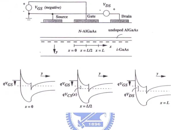
(45) discover the true RF performance of the device is discussed.. 3.2 DC characteristics [3-2]. The band diagrams at three different locations along the channel are illustrated in Fig. 3.1. There is a potential drop of channel charge density in the direction parallel to the channel, causing q’CH to be a function of the position x. In order to relate the HEMT equations to the well-developed MOSFET equations, a per area gate oxide capacitance was define as C’OX. [3.3] Therefore, the channel charge sheet density is expressed as: q'CH = −C 'OX [VGS − VT − VCS ( χ )]. (3-1). We denote the channel-to-source potential resulting from the applied Gate-Source voltage VGS and Drain-Source voltage VDS. VT is threshold voltage and the x means the position along the channel. The additional potential VCS(x) is called the channel-source potential. When VDS≠ 0, the channel channel-source varies with x. In this figure, the channel-source potential measures the potential difference between any point x along the channel with respect to the potential of the source. The channel current equation which we are familiar with I= qAµnε (A=area) is proportional to the cross-section area of the current conduction, the charge density, the mobility µn, and the electric field. Therefore, we obtain the form of the drift equation in HEMT: I CH ( χ ) = −WCOX µ n [VGS − VT − VCS ( χ )]. dVCS ( χ ) dχ. (3-2). We note that q’CH is a negative quantity in HEMT, since electrons accumulated in the channel are negative charges. In fact, if we choose x = L at the drain, this constant channel current is equal to the negative of the drain current. Hence, we have ID =- ICH, we find:. 27.
(46) ∫. L. 0. I DS dx = − C 'O. VCS ( L ). ∫C. OX. µ n [V ( GS ) − V (T ) − V ( CS ) ( χ )]dV CS ( χ ). (3-3). VCS ( O ). To carry out the integration in Eq. (3-3), we assume temporarily that we are working in the linear region such that current saturation due to channel pinch off at the drain does not occur. The I-V characteristics after pinch off will be dealt with shortly. In the linear operating region, the boundary conditions are VCS(L) = VDS and VCS(0) = 0. Hence, Eq. (3-3) leads to: ID =. W g C ' OX µ n V2 [(VGS − VT )VDS − DS ] 2 Lg. (3-4). Eq. (3-5) is plotted schematically in Fig. 3.2, with ID shown as a function of VDS. The value of VDS corresponding to the attainment of ID,sat is denoted as VDS,sat, the saturation voltage. The saturation voltage can be obtained by taking the derivative of ID will respect to VDS and setting the result to zero. We find that:. V DS , SAT = VGS − VT. (3-5). At this saturation voltage, q’CH calculated from Eq. (3-1) is identically zero at the drain (pinch off). However, we realize that this conclusion originates from the fact that we are extending the validity of Eq. (3-1) all the way to where q’CH(L) is identically zero. Physically, the channel at the drain does not pinch off completely. Instead, there is a finite thickness of accumulation of charges at which q’CH x=L is nonzero. The drift velocity is high, but nonetheless finite, so a constant current is maintained throughout the channel. Therefore, a complete model of the drain current is given by: I DS. 2 Wg C ' OX µ n VDS [(VGS − VT )VDS − ] = 2 Lg. for VDS < VDS,SAT. 28. (3-6).
(47) =. W g C ' OX µ n (V GS − VT ) 2 [ ] 2 Lg. for VDS ≧VDS,SAT. (3-7). For HEMTs, it is convenient to define the saturation index (α) as:. α = 1−. VDS VDS,SAT. for VDS < VDS,SAT. =0. for VDS ≧VDS,SAT. (3-8). The drain current increases due to the perturbations in VGS and VDS. The mutual transconductance measures the amount of current increase due to the increment in the gate bias. gm =. ∂I DS ∂VGS V = const . DS. We also can write:. gm =. W g C ' OX µ n (V GS − V T ) * (1 − α ) Lg. 3.3 Breakdown characteristics. Breakdown mechanisms and models have been discussed in many articles. One of the models showing it is dominated by the thermionic filed emission (TFE) / tunneling current from the Schottky gate. This model predicts that the two-terminal breakdown voltage is lower at higher temperature because tunneling current increases with the temperature. Higher tunneling current occurs at higher temperature because carriers have higher energy to overcome the Schottky barrier. Other model suggests that impact-ionization determines the final two-terminal breakdown voltage, because the avalanche current decreases with increasing temperature. Lower avalanche current occurs at higher temperature because phonon vibrations as well as carrier-carrier. 29.
(48) scattering increase with increasing temperature. Either model is incomplete since coupling exists between TFE and impact ionization mechanisms. In addition, different devices may suffer from different breakdown mechanisms, depending on the details of the device design (insulator thickness, recess, channel composition, and so forth). In this study, the gate-to-drain breakdown voltage BVgd is defined as the gate-to-drain voltage when the gate current is 1mA/mm.. 3.4 Scattering parameters [3-2]. Generally, the Scattering parameters, which referred to as S-parameters, are fundamental to microwave measurement. S-parameters are a way of specifying return loss and insertion loss. The relation of the microwave signals and s-parameters are defined as follows: ⎡b ⎤ ⎡s s-parameters: ⎢ 1 ⎥ = ⎢ 11 ⎣ b 2 ⎦ ⎣ s 21. s12 ⎤ ⎡ a 1 ⎤ ⎥*⎢ ⎥ s 22 ⎦ ⎣ a 2 ⎦. Microwave signals going into or coming out of the input port are labeled by a subscript 1. Signals going into or coming out of the input port are labeled by a subscript 2. The electric field of the microwave signal going into the component ports is designated a; that leaving the ports is designated b. Therefore, a1 is the electric field of the microwave signal entering the component input. b1 is the electric field of the microwave signal leaving the component input. a2 is the electric field of the microwave signal entering the component output. b2 is the electric field of the microwave signal leaving the component output. By definition, then,. s11 =. b1 a1 a 2 = 0 30.
(49) s 21 =. b2 a1 a 2 = 0. s12 =. b1 a 2 a1 = 0. s 22 =. b2 a 2 a1 = 0. Consequently, s11 is the electric field leaving the input divided by the electric field entering the input, under the condition that no signal enters the output. Because b1 and a1 are electric fields, their ratio is a reflection coefficient. Similarly, s21 is the electric field leaving the output divided by the electric field entering the input, when no signal enters the output. Therefore, s21 is a transmission coefficient and is related to the insertion loss or the gain of the device. s22 is similar to s11, but looks in the other direction into the device.. 3.5 Current gain cutoff frequency fT and maximum oscillation frequency fmax. The fT of a device is the frequency at which the short circuit current becomes unity. fT is defined as fT =. gm 2π (C gs + C gd ). , and the (Cgs + Cgd) is the total capacitance related to the Schottky gate contact. From this relation, we could see that in order to achieve high fT, large gm and small total gate capacitance must be achieved. Small total gate capacitance is accomplished by short gate length; for millimeter-wave applications the gate length is usually smaller than 0.15µm. In this equation fT =. gm Z v ε v w 1 = G sat • • = sat 2πCG w εZ G LG 2π 2πLG 31.
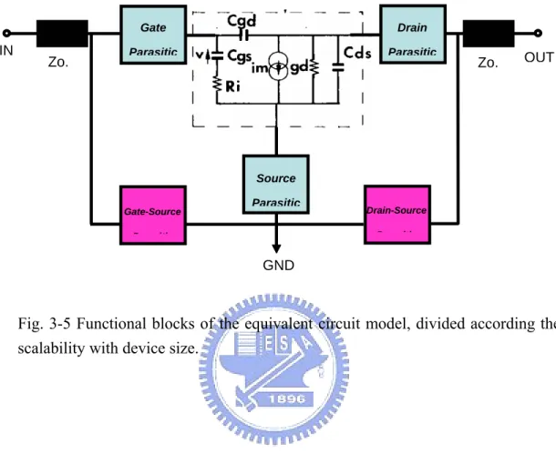
(50) the LG is the is the gate length; therefore, the shorter the gate length the higher the fT and higher the gm. The intrinsic S parameters are used to determine the unity current-gain cut-off frequency (fT). It can be determined by extrapolation of the short-circuit current gain h21 = 0 dB. h21 can be defined as h 21 =. 2 s 21 (1 − s11 )(1 + s 22 ) + s12 s 21. Another important parameter is fmax, which is the frequency where the power gain falls to unity. fmax is expressed as f max =. fT 1. ⎛ R + Ri + Rs ⎞2 2⎜⎜ g + ( 2πf T Rg C gd ) ⎟⎟ Rds ⎝ ⎠. This expression shows that to obtain useful power gain at high frequency, the fT of a device must be large; in addition, the resistances of gate, source and drain must be small.. 3.6 Device modelling technique. When defining the high frequency RF performance of the HEMTs, it is essential to de-embed all the conductors on the top surface of the wafer such as the pad, metal, and interconnect. Detailed layout of the device in this study is shown in Fig. 3-3. This helps us to understand what is going on at the active region of the device. A number of different semiconductor device models exist like small-signal, large-signal, and noise models. In this paper, an approach that combines the conventional way and 3-D full wave electromagnetic analysis is proposed and extracted the intrinsic parameters of devices. To accurately determine the equivalent circuit model, the overall structure is divided 32.
(51) into several blocks, including gate parasitic, drain parasitic, source parasitic and intrinsic part according to the scalability of the device size as shown in Fig. 3-4, where the parasitic elements should be kept at fixed values and not scalable with device size. The intrinsic block could further be divided into different equivalent circuit elements and shown in Fig. 3-5. Standard gradient optimization routine is used to minimize the error function value, which is defined as the difference between the modelled and measured S-parameters. Standard gradient optimization routine is used to minimize the error function value, which is defined as the difference between the modelled and measured S-parameters. In order to rigorously determine the parasitic elements, CST Microwave Studio which is based on finite integration algorithm in time domain (FIT) is applied to analyse the structure. It is observed from the filed plot that the two source buses are held at a lower potential referenced to the gate and source pads thus the E-filed lines tend to terminate at these buses indicating a strong capacitive parasitic (Fig. 3-6 a). To illustrate the difference, a similar structure without the two source buses is simulated and the electric filed at 10 GHz is plotted in Fig. 3-6 b, where a much coarser electric field distribution between the gate (drain) pad and source region is observed. Based on the EM analysis of the structure, the strong capacitive parasitic behavior between the gate (drain) pad and the source buses suggests two additional capacitors to be included in the equivalent circuit.. 3.7 Noise figure. High-frequency noise relates with the device channel and capacitive coupling between the channel and the gate. The gate noise is represented by a gate-current noise generator ing2 and is caused by charge fluctuation in the channel, which in turn induces the fluctuation of compensating charge on the gate electrode. The channel 33.
(52) noise is represented by a drain-current noise generator ind2 and is caused by various physical mechanisms driven by the electric field in the channel. Another noise source is gate leakage. The noise performance of a FET may be quantified by the noise figure, NF, which is a function of frequency, FET bias voltages, and impedance matching. NF can be well approximated by the semi-empirical equation given by Fukui [3-4] and is shown as the following equation: NF = 1+ k (f/fT) [gm (Rg+Rs)]1/2, = 1+ 2πkf (Cgs + Cgd) [gm (Rg+Rs)]1/2 , where k is a fitting parameter. Generally, the reduction in Lg does not necessarily minimize the NFmin because Rg tends to increase due to a vertical resistance component of gate resistance, and also gm decreases due to a degraded gate drive so-called “short-channel effect”. Therefore, a reduction in Rg and suppression of the short-channel effect are necessary to minimize NFmin.. 34.
(53) Fig. 3.1 Band diagrams at three different locations along the channel of a HEMT. 35.
(54) Eq. (3.4). Fig. 3.2 Actual characteristics and those predicted by Eq. (3-3). 36.
(55) Fig. 3-3 Detailed layout of the device, the pads connecting the gate and drain are about 50×100um2.. 37.
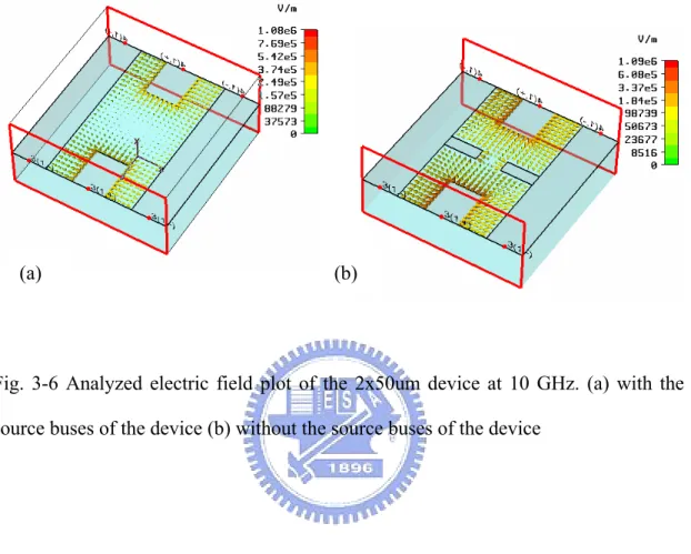
(56) Gate. IN. Intrinsic. Drain Parasitic. Parasitic. Zo,. Zo,. Source Parasitic Gate-Sourc. Drain-Sourc. e. e. GND Transmission line to accommodate for possible phase shift caused by probe positioning variation. Fig. 3-4 The block diagram with determined parasitic elements for the overall device structure.. 38.
(57) IN. Zo,. Gate. Drain. Parasitic. Parasitic. Zo,. OUT. Source Gate-Source P. Parasitic. Drain-Source P. iti. iti. GND. Fig. 3-5 Functional blocks of the equivalent circuit model, divided according the scalability with device size.. 39.
(58) (a). (b). Fig. 3-6 Analyzed electric field plot of the 2x50um device at 10 GHz. (a) with the source buses of the device (b) without the source buses of the device. 40.
(59) Chapter 4. RF. and. Logic. Performance. Improvement. of. In0.7Ga0.3As. /InAs/In0.7Ga0.3As Composite Channel HEMT Using Gate Sinking Technology. 4.1 Introduction. For the advanced wireless communications, InP-based high electron mobility transistors (HEMTs) have attracted many attentions and demonstrated excellent high-frequency performance because of its superior electronic transport properties and high saturation velocity [4-1, 4-2]. Moreover, it is also a potential candidate FETs for low-power logic applications beyond Si CMOS technology in 22 nm node era [4-3,4-4]. InP HEMTs usually use In-rich InGaAs channel or InAs/InGaAs composite channel for good RF performance with large current drivability of the device. Meanwhile, the gate-recess structure also plays a critical role in the high frequency performance for HEMT devices. In general, the transconductance (gm) of the device is mainly influenced by the gate-channel distance and the reduction of the distance can effectively increase the current gain cutoff frequency (fT) because of the enhancement of average electron velocity underneath the gate electrode. Additionally, the shape of the recessed region not only affects the source and drain resistance (Rs and Rd) and the capacitances of gate-source and gate-drain (Cgs and Cgd), but also modulates the electric field in the channel. K. Shinohara et al. reported fT value of 547 GHz in 30-nm gate pseudomorphic HEMTs by means of 41.
(60) multilayer cap structure to reduce parasitic source and drain resistances [4-5].. H.. Matsuzaki et. al. have employed Tiered-Edge Ohmic structure and low-k benzocyclobutene (BCB) passivation to effectively minimize parasitic gate capacitance and achieve relatively high gm and fT values [4-6]. Although the results seemed rather promising, yet relatively complicated fabrication processes were involved in the reduction of the parasitic elements. In this study, the In0.7Ga0.3As/InAs/In0.7Ga0.3As composite channel HEMTs were fabricated with Pt buried gate technology. The adoption of Pt buried gate is because Pt can diffuse into the barrier layer and the channel can be further recessed [4-7 – 4-9]. The diffused gate has lower parasitic capacitance and resistance as compared to that of the recessed gate. Additionally, the Pt has higher metal work function (5.65eV) than that of Titanium (4.1eV).. The measurement results in this study clearly. evidenced that superior device performance can be achieved through very simple and straightforward gate sinking fabrication process with optimal epi structure as compared to those proposed in [4-5] and [4-6].. 4.2 Experiment. The HEMT structure was grown by molecular beam epitaxy on a 2-in diameter InP substrate. The schematic of the structure is shown in Fig.1 and given as follows, a 50-Å InAs channel layer with 20-Å In0.7Ga0.3As upper subchannel and 30-Å In0.7Ga0.3As lower subchannel were grown on top of the 500-nm-thick InAlAs buffer layer. The In0.7Ga0.3As sub-channels were applied to enhance the electron confinement in the thin InAs layer and improve the electron transport properties [4-10]. A 40-Å-thick InAlAs spacer, a Si-δ-doping with 5×1012 cm-2, a 10-nm-thick InAlAs barrier. A 4-nm-thick InP etching stop, and a 35-nm-thick InGaAs cap layer 42.
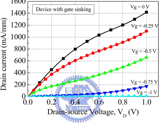
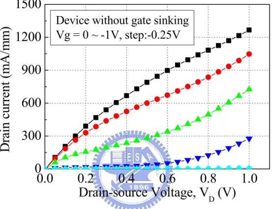
(61) with 2×1018 cm-3 Si-doping were grown on top of the composite channel layers. For the device fabrication, the active area of the device was isolated by wet etch. The ohmic contacts were formed with 3 µm source-drain spacing by evaporating Au/Ge/Ni/Au on heavily doped n-InGaAs cap layer and then alloyed at 250oC for 25 second to attain low contact resistance (Rc). For the T-shaped gate process, it was performed by the 50kV JEOL electron beam lithography system (JBX 6000 FS) with trilayer e-beam resist. Succinic acid/H2O2/NH4OH solution was used for gate recess and then Pt (12nm)/Ti (60nm)/Pt (80nm)/Au (180nm) were deposited as Schottky gate metal and lift off by ZDMAC to form 80-nm T-shaped gate. The insert SEM image is the unpassivated T-shaped gate formed after recess. A 100-nm thick silicon nitride was deposited as passivation layer by PECVD at 250oC for 10 min. Finally, thermal annealing at 250oC for 3 minutes in forming gas ambient was carried out for gate sinking to further recess the channel. The contact resistance was 0.032 Ω‧mm after gate sinking process, which remained almost unchanged as compared to that of 0.021 Ω‧mm before annealing.. 4.3 Result and Discussion. Fig. 2 shows the DC I-V curve of the device with 2×50 µm gate width using gate sinking technology. The device exhibited very good pinch-off characteristic and the saturation current of 1418 mA/mm at VDS = 1V and Vgs = 0V as compared to the drain current of 1267 mA/mm for device before gate sinking showed in Fig. 3. This very high drain current density was mainly due to the superior electron mobility in the In0.7Ga0.3As/InAs/In0.7Ga0.3As composite channel and the non-degrading performance of the ohmic contact during gate annealing. In addition, the gate sinking occurrence might cause the decrease of the drain current. In this studied, although the gate 43.
(62) sinking occurred, the drain current increased. The extracted values of source resistance Rs was 1.35 Ω for device without gate sinking compared to 1.22Ω for device with gate sinking. As a result, it is conclude that the reduction of parasitic resistance by the suppression of the formation of surface traps is the main reason for the performance enhancement of the device, because the increase in current is as high as 151 mA/mm [4-10]. As for the gate-drain breakdown voltage (VDG,BR), the value decreased from 3.6V for device without sinking (Fig. 4a) to 2.4V for that with sinking (Fig. 4b), which is mainly due to the reduction in the Schottky barrier thickness after gate sinking process. The transconductance gm and the drain source current plotted as functions of Vgs for devices without and with gate annealing are included in Fig. 5. As is observed from the figure, the peak gm value has increased from 1470 mS/mm for the device without gate sinking to 1590 mS/mm for that with gate sinking, both measured at VDS = 0.5 V. This increase is mainly attributed to the sinking of Pt atoms into the InP etching stop layer which in turn shifted the gate metal front closer to the two-dimensional electron gas (2DEG) channel. Meanwhile, the threshold voltage shifted from -0.91 (without gate sinking) to -0.8 V (with gate sinking) when biased at VDS = 0.5V. The threshold voltage is defined as the Vgs when Ids reaches 1mA/mm. A slight reduction in the gate leakage current from 1.66 × 10⁻⁶ A (without gate sinking) to 6.3 × 10⁻⁷A (with gate sinking) was also observed when biased at VDS = 0.8V and Vgs = 0V owing to the increase in the thickness of the amorphous layer under gate which diminished the leakage path because of the reduction of the grain boundaries [4-8], [4-11]. The S-parameters of the 2×50 µm device were measured from 5 to 80 GHz using on-wafer probing system with HP8510XF network analyzer. Fig. 6 and Fig. 7 show the frequency dependence of the current gain H21, the power gain MAG/MSG, and the 44.
(63) Mason’s unilateral gain U of the device with/without gate sinking measured at VDS = 0.8V and Vgs = -0.5V. The parasitic effects (mainly capacitive) due to the probing pads have been carefully removed from the measured S-parameters using the same method as in [4-12] and the equivalent circuit model in [4-13]. Since the geometry of the probing pads are relatively large compared to the device itself, the S-parameters of the open probing pads have been carefully characterized through full-wave electromagnetic simulations with measurement. Standard gradient optimization routine with tolerance level of delta S less than 0.01% were set as the convergence criterion during the fitting process. The capacitance at the gate-source end was extracted to be 10.2 fF and the capacitance at the gate-drain end was about 8.6 fF. The extracted gate resistance was about 4Ω. A very high current gain cut-off frequency fT of 494 GHz and the maximum oscillation frequency fmax of 390 GHz were obtained for device with sinking as compared to that of fT = 390 GHz and fmax = 360 GHz for the device without sinking. This improvement in the RF performance was due to the increase of gm and the decrease of the gate-to-source capacitance (Cgs) in the applied gate bias range resulting from the gate sinking process. This decrease in Cgs was also evidenced from the measured S-parameters (even before the removal of parasitic elements) where a S11 contour with smaller “radius” with respect to the center of Smith Chart was observed as shown in Fig. 8, indicating a small capacitance value seen at the input port. Similar trend of reduction in (Cgs) values due to gate sinking process has also been observed in [4-14]. Table 4.1 summarizes the extracted intrinsic parameters for devices with and without gate sinking at same bias conditions. The increase in fT is mainly caused by the decrease of Cgs and increase of the transcondutance. The noise performances for devices with/without gate sinking at drain voltage biases VDS = 0.3 V, and VDS = 0.1 V are shown in Fig. 4-9 and 4-10 with frequency 45.
數據
+7
相關文件
Elements of Computing Systems, Nisan & Schocken, MIT Press, www.nand2tetris.org , Chapter 9: High-Level Language slide 2.. Where we
Elements of Computing Systems, Nisan & Schocken, MIT Press, www.nand2tetris.org , Chapter 9: High-Level Language slide 2.. Where we
FUEL LEVEL TRANSMITTER: Low Level Fuel Pressure : High Pressure TRANSFER PUMP SWITCH : ON. 與繼電器 K1 串聯之 Blocking
• 接續之前的例子,若原為 0.288 pF 的液晶 電容 C LC ,再並聯一個亦為 0.288 pF 的電 容C st ,則電位保持的變化值為.
觀念學習一 速率公式的變化 對應能力指標. 6-n-08
“Polysilicon Thin Film Transistors Fabricated at 100℃ on a Flexible Plastic Substrate,” IEEE Electron Device Meeting, p. “Polysilicon Thin Film Transistors
method void setInt(int j) function char backSpace() function char doubleQuote() function char
This paper presents a calibration technique which estimates the mismatch, and adjusts the equivalent gain of the phase noise canceling circuitry to improve the degree of phase
