超薄氧化層絕緣層上覆矽元件中軟式崩潰所引發之可靠性議題的探討
125
0
0
全文
(2) 超薄氧化層絕緣層上覆矽元件中軟式崩潰 所引發之可靠性議題的探討 研究生: 陳旻政 國立交通大學. 指導教授: 汪大暉博士 電子工程學系. 電子研究所. 摘要 當積體電路製程推進到奈米(sub-100nm)元件世代,絕緣層上覆矽 技術的使用將是可行性的替代方案之一。當元件尺寸縮小到 100 奈米 時,閘極介電層的等效氧化層厚度必須薄於 20 埃以下。然而,在如 此薄氧化層的絕緣層上覆矽元件中,軟式崩潰所引發之可靠性問題將 是異常重要。 本篇論文將針對超薄氧化層絕緣層上覆矽金氧半場效電晶體中 軟式崩潰所引發之可靠性議題作一系列的探討。首先,吾人探討超薄 閘極氧化層中直接穿隧區域的電荷傳輸機制。主要的閘極穿隧漏電流 可以分成源/汲極穿隧電流和基底極穿隧電流。在此吾人利用一套量 子化電荷傳輸機制來解釋源/汲極電流和用古典的電荷傳輸機制來解 釋基底極電流。為了精準的模擬穿隧電流,吾人藉由解波松和薛丁格 聯立方程式來計算氧化層電場。在超薄氧化層絕緣層上覆矽金氧半場 效電晶體中,由於浮動基底極的原因,這些穿隧漏電流將對可靠性造 成一些新奇的影響。 接下來,在浮動基底極絕緣層上覆矽元件中,吾人知道大量的基 底漏電流所造成的基底電位的調變和所導致不可避免的磁滯效應已. i.
(3) 被廣泛的討論。由於氧化層崩潰將增加基底極的穿隧漏電流,所以在 浮動基底極的超薄閘極氧化層絕緣層上覆矽元件中,崩潰位置對臨界 電壓磁滯現象的影響將在這部分探討。吾人將發表兩種在關閉狀態的 金氧半電晶體中氧化層崩潰增強磁滯現象的模型。吾人所提供的基底 充電機制和實驗結果相符。在浮動基底結構下的超薄閘極氧化層部份 空乏絕緣層上覆矽金氧半場效電晶體中,軟式崩潰增強的磁滯現象將 成為一種嚴重的可靠性議題。 再者,吾人發現在浮動基底絕緣層上覆矽金氧半場效電晶體中通 道軟式崩潰導致一種新的低頻汲極電流雜訊退化現象。這種額外的雜 訊來源來自於通道軟式崩潰導致大量基底極的價帶電子穿隧電流產 生微量的白雜訊放大所致。在超薄閘極氧化層類比絕緣層上覆矽元件 中,即使在操作電壓小於一伏特,通道軟式崩潰增加額外的雜訊仍會 發生並將成為一個重要的可靠性問題。 最後,直接穿隧效應也會對超薄氧化層的崩潰及元件之毀壞產生 影響。一般來說,元件的毀壞與否是由氧化層崩潰所造成破壞程度所 決定,代表破壞程度較低的氧化層漏電流對實際電路應用而言,並不 會造成任何操作上的影響。吾人在 p 型超薄氧化層絕緣層上覆矽電晶 體中,針對浮動基底極對氧化層崩潰的破壞程度作完整之研究。在 p 型超薄氧化層元件中,吾人發現了正偏壓基底極操作模式下所產生的 加速崩潰破壞。當氧化層初崩潰時,高能量的通道電洞在正偏基底極 時產生較大的電動加壓電流,進而使得氧化層產生更大的破壞。藉由 熱載子光激發實驗及熱電洞在通道能階上的分佈分析,吾人成功地解 釋出此基底極偏壓相依性。吾人並預測此種崩潰破壞將對浮動基底超 薄閘極氧化層絕緣層上覆矽 p 型金氧半場效電晶體產生新的可靠性 議題。. ii.
(4) Investigation of Soft Breakdown Induced Reliability Issues in Ultra-Thin Oxide SOI Devices. Student: Min-Cheng Chen. Advisor: Dr. Tahui Wang. Department of Electronics Engineering & Institute of Electronics, National Chiao-Tung University Hsinch, Taiwan, R.O.C.. Abstract. The silicon-on-insulator (SOI) technology is a promising candidate of IC manufacture required for sub-100nm CMOS devices. As device size shrinks below 100nm, the effective oxide thickness of gate dielectric must scale below 20Å. While, a great reliability concern induced by soft breakdown (SBD) in such thin oxides SOI devices is being aroused. The objective of this dissertation is to investigate soft breakdown induced reliability issues in such ultra-thin oxide SOI MOSFETs. First of all, the charge transport mechanisms of oxide in direct tunneling regime is investigated. The gate tunneling leakage current can be separated by source/drain tunneling current and substrate tunneling current. In this work, a quantum charge transport mechanism is proposed to explain the source/drain current. And, a classical charge transport mechanism is proposed to explain the substrate current. To calculate the tunneling current accurately, the oxide electric field is simulated by means of solving the combined Poisson and Schrodinger equations. These tunneling leakage currents may bring about some reliability concerns in floating body ultra-thin oxide SOI. iii.
(5) MOSFETS. Further, substrate leakage current has been known to cause substrate bias variation and induce unavoidable hysteresis effects in floating body SOI devices. Since oxide breakdown can enhance substrate tunneling leakage current, the impact of breakdown location on threshold voltage hysteresis in ultra-thin oxide SOI devices is investigated in this part. Two breakdown enhanced hysteresis modes in off-state CMOS are identified. The proposed body charging mechanisms are verified by our measurement results. The SBD enhanced hysteresis effect would be a serious reliability subject in ultra-thin oxide MOSFETs with floating body configuration. Moreover, a new low frequency drain current noise source in floating body SOI nMOSFETs caused by channel soft breakdown is studied. The excess noise originates from channel soft breakdown enhanced valence band electron tunneling and the amplification by the small white noise of the substrate current. The c-SBD enhanced excess noise may occur even with supply voltage less than 1.0V and would be an important reliability problem in analog applications. Finally, a large direct tunneling current can decrease oxide time-to-breakdown and limit oxide further scaling. Actually in most circuits, the failure criterion is determined by the hardness of oxide breakdown. In this part, floating body enhanced breakdown progression in ultra-thin oxide SOI pMOS is proposed. The enhanced progression is attributed to the increase of hole tunneling current resulting from breakdown induced channel carrier heating. The substrate bias dependence of post-breakdown hole tunneling current is confirmed through the calculation of channel hole distribution in sub-bands. This observed phenomenon is significant to ultra-thin gate oxide reliability in floating body SOI pMOSFETs.. iv.
(6) 致謝 首先,這本博士論文的完成,必須感謝我的指導老師汪大暉教 授。他有深厚的理論基礎,再加上細心與耐心的指導態度,使得我很 容易從他的隻字片語中學習到新的知識及觀念。最重要的是,在他身 上感受到對學術的熱忱,並學習到做學問的方法和應有的嚴謹態度, 以及面對問題時,該如何抽絲剝繭,最終能接近真相。 在論文的研究上必須感謝許多曾經指導過我的許多學長,及一起 參與研究的同學及學弟。首先感謝蔣汝平、鄒年凱、陳奇祥、易成名、 及陳尚志學長在我剛進研究生活的指導與鼓勵。同時,我也感謝古紹 泓、詹前泰、鄭志昌及游建文學弟在實驗執行上的幫助。也要感謝聯 華電子提供我做研究的空間和王木俊經理、黃呂祥經理、李明燦經 理、楊國璽經理、葉名世經理、唐天浩經理及元昌大哥提供我研究上 相關的協助及意見。 其次,感謝前瞻元件與技術實驗室的全體學弟妹,有了你們,實 驗室充滿了歡樂。此外,聯華電子 CRD_RS 的所有同仁們,對我的照 顧及愛護,再此我要說一聲謝謝。還有王志馨、蔡慶威及吳俊威等陪 伴我度過這段求學生涯中的好朋友,沒有你們的陪伴與勉勵,我無法 如此順利的畢業,我也要在此獻上我最誠摯的感謝。 另外,感謝我的父母、家人,在我攻讀博士班期間給我的鼓勵與 支持,有他們在背後無怨無悔的付出與關心,讓我毫無顧忌的專注於 論文研究,使得這本博士論文得以順利完成。 最後,謹將這份榮耀獻給我最親愛的父母。. v.
(7) Contents Chinese Abstract. i. English Abstract. iii. Acknowledgements. v. Contents. vi. Figure Captions. ix. Table Captions. xiv. Chapter 1. Introduction. Chapter 2. Simulation of Charge Transport in Ultra-Thin. 1. Oxide MOSFETs. 5. 2.1. Introduction. 5. 2.2. Surface Quantization and Gate Capacitance Modeling. 6. 2.3.1 Simulation Model for Potential Distribution. 6. 2.3.2 Self Consistent Solution of Schrodinger's and. 2.3. 2.4. 2.5. Poisson's Equations. 8. 2.3.3 Gate Capacitance Modeling. 8. Source/Drain Tunneling Current Modeling. 17. 2.3.1 Transport of Conduction Band Electrons. 17. 2.3.2 Simulated and measured results. 20. Substrate Tunneling Current Modeling. 25. 2.4.1 Transport of Valence Band Electrons. 25. 2.4.2 Simulated and Measured Result. 26. Summary. 27. vi.
(8) Chapter 3. Chapter 4. Soft Breakdown Enhanced Hysteresis Effects in Ultra-Thin Oxide SOI MOSFETs. 31. 3.1. Introduction. 31. 3.2. Device Structure and Characterization. 32. 3.3. Modes of SBD Enhanced Hysteresis. 38. 3.4. Results and Discussion. 41. 3.5. Summary. 42. Soft Breakdown Enhanced Excess Low- Frequency Noise in Ultra-Thin Oxide SOI n-MOSFETs. 50. 4.1. Introduction. 50. 4.2. Excess Low-Frequency Noise Model in SOI MOSFETs. 51. 4.3. Kink Effect Induced Excess Low-Frequency Noise. 60. 4.4. Channel Soft Breakdown Enhanced Excess Low-. 4.5. Chapter 5. Frequency Noise. 66. Summary. 68. Floating Body Accelerated Oxide Breakdown Progression in Ultra-Thin Oxide SOI p-MOSFETs. 73. 5.1. Introduction. 73. 5.2. Devices and Experiment. 74. 5.3. Result and Discussion. 76. 5.3.1 A Shorter tfail in SOI pMOSFETs. 76. 5.3.2 Mechanism of Enhanced BD Progression in SOI. 76. 5.3.3 BD Caused Carrier Heating. 77. vii.
(9) Chapter 6. 5.4. The Impact of Gate Stress Bias. 88. 5.4. Summary. 88. Conclusions. 93. References. 95. Vita. 108. Publication Lists. 109. viii.
(10) Figure Caption. Fig. 2.1. Algorithm to solve Poisson's and Schrodinger's equations self-consistently.. Fig. 2.2. Sub-band wave-functions in substrate calculated from a pre-guessed potential.. Fig. 2.3. Six state wave-functions and energy levels from a pre-guessed potential.. Fig. 2.4. Electron distributions calculated from classical and quantum-mechanical models.. Fig. 2.5. Hole distributions calculated from classical and quantum-mechanical models.. Fig. 2.6. Measured and simulated C-V curves of an n-MOSFET device.. Fig. 2.7. Measured and simulated C-V curves of a p-MOSFET device.. Fig. 2.8. Illustration of source/drain tunneling current components in MOSFET's in strong inversion condition.. Fig. 2.9. Measured and simulated Isd-Vg curves of an n-MOSFET device.. Fig. 2.10 Measured and simulated Isd-Vg curves of a p-MOSFET device. Fig. 2.11 Illustration of substrate current transport in MOSFET's in strong inversion condition. Fig. 2.12 Measured and simulated Ib-Vg curves of an n-MOSFET device. Fig. 2.13 Measured and simulated Ib-Vg curves of a p-MOSFET device. Fig. 3.1. Gate current and substrate current versus gate bias in nMOSFETs. Solid line refers to an unstressed device and dashed line (dotted line) refers to a device after channel SBD (drain edge SBD).. Fig. 3.2. Body current versus drain bias in nMOSFETs. Solid line refers to an unstressed device and dashed line (dotted line) refers to a device after channel SBD (drain edge SBD).. ix.
(11) Fig. 3.3. Gate current and substrate current versus gate bias in pMOSFETs. Solid line refers to an unstressed device and dashed line (dotted line) refers to a device after channel SBD (drain edge SBD).. Fig. 3.4. Illustration of two soft-breakdown enhanced floating-body charging processes in SOI nMOSFETs. (a) soft breakdown in the channel region and hole creation due to valence band electron tunneling; (b) soft breakdown in the drain region and enhanced GIDL current.. Fig. 3.5. Illustration of two soft-breakdown enhanced floating-body charging processes in SOI pMOSFETs. (a) soft breakdown in the channel region and valence band electron tunneling from poly-gate to the floating body; (b) soft breakdown in the drain region and enhanced GIDL current.. Fig. 3.6. Hysteresis in Ids and corresponding floating-body potential versus Vg in a c-SBD SOI nMOSFETs. Measurement is performed with forward and then reverse drain sweeps from 0V to 1.3V.. Fig. 3.7. Hysteresis in sub-threshold current and corresponding floating-body potential in an e-SBD SOI nMOSFETs. Measurement is performed with forward and then reverse drain sweeps from 0V to 1.3V.. Fig. 3.8. The variation of body voltage Vb as a function of the amplitude of gate bias sweep in SOI nMOSFETs. Vd=0V.. Fig. 3.9. The variation of body voltage Vb as a function of the amplitude of drain bias sweep in SOI nMOSFETs. Vg=0V.. Fig. 3.10 The variation of body voltage Vb as a function of the amplitude of gate bias sweep in SOI pMOSFETs. Vd=0V. Fig. 3.11 The variation of body voltage Vb as a function of the amplitude of drain bias sweep in SOI pMOSFETs. Vg=0V. Fig. 3.12 Illustration of dominant Vt hysteresis modes in the switching of an SOI CMOS inverter.. x.
(12) Fig. 4.1. Noise sources in an SOI MOSFET.. Fig. 4.2. (a) Noise small-signal equivalent circuit for the floating-body and (b) schematic for the req and Ceq network.. Fig. 4.3. Typical input-referred low-frequency noise spectrum.. Fig. 4.4. Low-frequency noise measurement setup.. Fig. 4.5. The Id-Vd characteristics in nMOS SOI devices with floating body and grounded body when gate is biased at 0.9V.. Fig. 4.6. Normalized noise power spectral density in floating body nMOS SOI devices under different drain voltages with gate biased at 0.9V.. Fig. 4.7. Normalized noise power spectral density in grounded body nMOS SOI devices under different drain voltages with gate biased at 0.9V.. Fig. 4.8. Comparison of normalized noise power spectral density under different drain biases in floating body SOI devices and grounded body SOI devices at given frequency.. Fig. 4.9. The gate current and substrate current as a function of Vg in fresh, channel SBD, and edge SBD n-MOSFETs are compared.. Fig. 4.10 The low frequency drain noise spectrums of a n-MOSFET before and after two SBD modes. The measurement drain bias is 0.1V and the gate bias is 1.2V. Fig. 4.11 The normalized noise power spectrum of a c-SBD nMOS SOI device with floating body under different gate biases. Fig. 4.12 Comparison of normalized noise power spectral density with floating body under different gate biases in a fresh device, c-SBD device and e-SBD device at f=100Hz. Fig. 5.1. Comparsion of breakdown behavior in a 1.4nm oxide pMOSFETand in a 2.5nm oxide pMOSFET. The stress gate voltage is –3V for the 1.4nm. xi.
(13) oxide and –4.5V for the 2.5nm oxide. tBD denotes the onset time of oxide breakdown. Fig. 5.2. Oxide breakdown progression in bulk and SOI pMOSFETs. The stress gate bias is –2.9V and temperature is 125o C.. Fig. 5.3. The Weibull plots of tBD and tfail distribution for 1.6nm oxide SOI and bulk pMOSFETs. The stress gate bias is –2.9V and the temperature is 125o C. tBD and tfail are defined as the time for gate current to reach 1.5 times and 15 times of its pre-stress value, respectively.. Fig. 5.4. The Vb dependence of pre-BD and post-BD electron currents (Ib) and hole currents (Isd) at Vg=-1.5V. Distinct Vb dependence of the post-tBD Isd is noted. The floating body configuration corresponds to a body voltage of approximately -0.65V. The inset illustrates carrier flow in a pMOSFET at a negative gate bias.. Fig. 5.5. The Vb dependence of the hole current Isd at different stress times, t0, t1, t2 and t3. Isd is normalized to its value at Vb=2V. Gate current vs. stress time in a stress condition of Vg=-3.2V and T=25o C is shown in the inset.. Fig. 5.6. Spectral distribution of light emission in a 1.4nm oxide pMOSFET at Vg=-2.5V. The extracted carrier temperature from the high-energy tail of the spectrum is around 1300 o K.. Fig. 5.7. Illustration of hole distribution in sub-bands at a hole temperature of 300 o K and 1300 o K. Higher carrier temperature results in a larger Vb effect.. Fig. 5.8. Simulated substrate bias effect on hole tunneling current in a 1.6nm oxide pMOSFET. Isd is normalized to its value at Vb=2V. Simulated Vg=-1.5V.. Fig. 5.9. Substrate bias dependence of the post-BD hole current at various gate biases. Isd is normalized to its value at Vb=2V.. Fig. 5.10 Gate bias dependence of electron current and hole current in a fresh pMOSFET and during progressive BD.. xii.
(14) Fig. 5.11 tfail (63%) vs. gate stress bias for SOI and bulk pMOS devices. Fig. 5.12 The range of oxide thickness and stress gate voltage where the hole current component is dominant in a fresh device and after breakdown. h or e represents hole current or electron current dominant regime, respectively.. xiii.
(15) Table Caption. Table 3.1 The ratio of Id/(Is+Id) and Ib/(Is+Id) before and after soft breakdown in four SOI MOSFETs. The measurement is in the accumulation region and Vg= |1.5V|, Vd=Vs=0V.. Table 5.1 Calculated distributions of channel holes in the lowest three sub-bands. The gate bias in simulation is –1.5V. The parameters used in simulation is m*(Si) = 0.67m0, m*(SiO2) = 0.55m0, φh (hole barrier height at SiO2 interface) = 4.25eV, tox = 1.6nm, and NB (substrate doping) = 1x1018cm-3.. xiv.
(16) Chapter 1 Introduction Gate oxide thickness scaling has been recognized as one of major keys in CMOS device scaling. With the device shrinkage, gate oxides below 2 nm are needed for sub-100nm CMOS technology. It is amazing that such thin oxide doesn’t suffer much from extrinsic factors such as defect density, surface roughness and uniformity control. The physical limitation of oxide thickness is caused by quantum-mechanical tunneling of carriers. The direct tunneling current increases exponentially by about one order of magnitude for every 2~3Å reduction in oxide thickness [1.1]. Large tunneling currents with device scaling make oxide breakdown play an important role in reliability issues. Additionally, silicon-on-insulator (SOI) CMOS has been emerged as one promising solution to increase the performance of CMOS over that offered by simple scaling.[1.2,1.3] In bulk CMOS, the oxide soft breakdown (SBD) just increases the tunneling leakage current and does not disrupt circuit operation.[1.4] In fact, this unnecessary leakage current not only causes increased power dissipation but also may bring about some reliability subjects such as hysteresis effects, noise degradation and oxide breakdown in ultra-thin oxide SOI CMOS devices. Partially Depleted (PD) SOI MOSFETs have the advantages in better threshold voltage control and easier fabrication process than fully depleted SOI MOSFETs. However, the floating body configuration of PD SOI MOSFETs has aroused several serious problems in device characteristics. An excess substrate leakage current can charge the substrate and cause annoying hysteresis effects. The SBD enhanced substrate tunneling leakage current may make the hysteresis effects more serious in PD SOI CMOS. The influence of SBD location on hysteresis effects in PD SOI MOSFETs will be investigated in various device operation modes. High performance SOI MOSFETs have been the primary platform of RF and microwave. 1.
(17) analogy circuits due to reduced junction capacitance and also due to the benefits of a high receptivity substrate.[1.5,1.6] Low-frequency noise is a key design constraint and an important figure-of-merit in analogy MOS circuits. Moreover, unwanted floating-body effects including the excess low-frequency noise have been extensively studied for SOI MOSFETs.[1.7,1.8] In this thesis, we will explore the noise properties of PD SOI MOSFETs in different SBD modes. The impact of SBD location on low frequency noise in SOI devices will be investigated in this thesis, too. Time dependence dielectric breakdown (TDDB) is an important reliability index of ultra-thin gate oxide. Although stress oxide field of SOI MOSFETs is not varied by floating body induced forward substrate bias, the negative substrate bias may enhance the pMOS breakdown progression.[1.9,1.10] The comparison of breakdown hardness in SOI and bulk pMOSFETs will be discussed in this thesis. Our result shows that oxide breakdown rate is enhanced in SOI devices. This points toward that SBD will be an urgent reliability issue in ultra-thin PD SOI MOSFETs.. Organization of this Thesis This thesis is organized into six chapters. Following the introduction, the gate tunneling leakage current in n- and p- MOSFETs with ultra-thin oxide is calculated in Chapter 2. The gate leakage current contains quantum charge transport of inversion carrier (source/drain tunneling current, Isd) and classical charge transport of valance band electron (substrate tunneling current, Ib). To calculate charge transport accurately, the Poisson and Schrodinger equations are solved self-consistently. The carrier energy quantization and corresponding wave-functions in the inversion layer are obtained from the Schrodinger equation. The ploy-gate depletion effect is investigated by solving the Poisson equation. A modified WKB approximation for charge transmission probability is employed in the calculation of the tunneling leakage current. The simulation of. 2.
(18) C-V curves is also identified in this chapter. The impact of oxide soft breakdown location on threshold voltage hysteresis in PD SOI MOSFETs with an ultra-thin oxide is investigated in Chapter 3. Two breakdown enhanced threshold voltage hysteresis modes are identified. In a drain-edge breakdown device, excess holes resulting from band-to-band tunneling flow to the floating body, thus causing threshold voltage variation in drain bias switching. In contrast, in a channel breakdown device, enhanced threshold hysteresis is observed during gate bias switching because of increased valence band electron tunneling. Our findings reveal that soft breakdown enhanced hysteresis effects can be a serious reliability issue in ultra-thin oxide SOI devices with floating body configuration. In Chapter 4, a new low frequency noise degradation mode in nMOSFETs due to breakdown enhanced floating body effect is proposed. In a channel breakdown device, a noise overshoot phenomenon is observed in the ohmic regime. It is characterized by a peak in drain current noise spectral density versus the operation gate voltage, whereby the peak amplitude can be about one order of magnitude higher than the background 1/f noise. In addition, it is shown that the corresponding spectrum has a Lorentzian shape. The origin of this excess noise is due to c-SBD enhanced valance band electron tunneling induced amplification of the substrate shot noise. The excess low frequency noise model in SOI MOSFETs is also proposed. The findings indicate that c-SBD enhanced drain current noise can be a reliability issue in PD analog SOI CMOS circuit. In Chapter 5, enhanced oxide breakdown progression in ultra-thin oxide SOI pMOS is observed, as compared to bulk devices. The enhanced progression is attributed to the increase of hole stress current resulting from breakdown induced channel carrier heating in a floating-body configuration. Numerical analysis of hole tunneling current and hot carrier luminescence measurement are performed to support our proposed theory. This phenomenon is particularly significant to the reliability of floating body SOI pMOS with thinner oxides and. 3.
(19) lower gate voltage. Conclusions are finally made in Chapter 6.. 4.
(20) Chapter 2 Simulation of Charge Transport in Ultra-Thin Oxide MOSFETs 2.1 Introduction With the continuing device scaling, gate oxides below 20Å are needed for sub-100nm CMOS technology [2.1]. In such small devices, the oxide field reaches a maximum of 5MV/cm, while the field in silicon exceeds 1 MV/cm [2.2,2.3]. The operation of deep-sub micron MOSFETs is entering a regime where quantum-mechanical effects become noticeable and classical physics is no longer sufficient for accurate modeling of device characteristics. The finite thickness of the inversion/accumulation layer (mostly due to quantum-mechanical effects) causes a significant discrepancy between calculated oxide capacitance and measured result [2.4]. In addition, as the surface electric field continues to increase due to oxide thickness scaling, the poly-silicon gate depletion effects appear to be more significant [2.5]. The depletion can further reduce the measured gate capacitance and degrade the charge control capability for a given gate bias. Furthermore, substantial charge tunneling through the gate insulator takes place even at operating biases as low as 1-1.5V. This gate leakage current increases exponentially as the oxide thickness is decreased and eventually becomes a limiting factor in device off-state leakage. Consequently, future low-voltage circuits may operate with considerable gate-oxide tunneling [2.6]. Therefore, the tunneling behavior of carriers through ultra-thin oxides must be well understood for future technology development. In this chapter, the C-V and I-V characteristics of ultra-thin oxide n- and p-MOSFETs will be simulated and measured. A quantum-mechanical approach is developed to study some major concerns for ultra-thin oxide MOS structures, such as surface quantization and poly-gate depletion. The Poisson and the effective-mass Schrodinger equations are solved self-consistently in our simulation. Simulated results are found to be in agreement with experimental results. In this work, the devices have a large area (3µm*300µm) and the C-V. 5.
(21) and I-V measurements are performed by using HP 4284 and HP4156B.. 2.2 Surface Quantization and Gate Capacitance Modeling In this section, we will discuss the Schrodinger and the Poisson equations first. Then, we will show the flowchart for a self-consistent solution of those equations. Finally, the measurement and simulation results of C-V curve will be presented and discussed.. 2.2.1 Simulation Model for Potential Distribution When energy bands are bent strongly near the Si substrate surface, the potential well formed by the surface barrier and the electrostatic potential in the Si substrate is sufficiently narrow that quantum-mechanical effects become important [2.7]. Only a single carrier needs to be treated quantum-mechanically when confined by the surface potential. For example, at a positive gate bias in a nMOSFET only surface electrons have quantum confinement effect while the surface holes do not exhibit quantization effects. When the carriers are confined, the electrical characteristics of an MOS structure should be modeled by solving the coupled effective-mass Schrodinger (in the oxide and silicon regions) and Poisson equations (in the poly-silicon, gate dielectric, and silicon regions) self-consistently. A closed quantum mechanical system is assumed, i.e., the tunneling current in oxides is neglected while solving the Schrodinger equation [2.8,2.9]:. h2 d 1 d [− + V ( z ) − Eij ]ψ ij ( z ) = 0 2 dz mi * dz. and. 6. (2-1).
(22) d d q − + [ε ( z ) ]ϕ ( z ) = [n( z ) − p( z ) + N A − N D ] dz dz ε0. (2-2). where z is the direction perpendicular to the channel, mi* is the electron effective mass in the ith valley , ψij is the envelope wave function for the jth sub-band in the ith valley, V is the potential energy, and NA- and ND+ are respectively the ionized acceptor concentration and donor concentration. The potential energy V(z) in Equation (2-1) is related to the electrostatic potential ϕ(z) in Equation (2-2) as follows:. V ( z ) = − qϕ ( z ) + ∆EC ( z ). (2-3). where EC(z) is the energy due to the band offset at the Si/SiO2 interface. The wave function ψ(z) [2.10] in Equation (2-1) and the electron density n(z) in Equation (2-2) are related by. n( z ) =. k BT πh 2. ∑ g m *∑ ln[1 + exp(( E i. i. di. − Eij ) / k BT ))]ψ ij ( z ) 2. f. (2-4). j. where gi and mdi* are the ith valley degeneracy and the ith density-of-states effective mass. The equations describing hole quantization are similar to Equations (2-1)-(2-4). The dielectric constant ε(z) is 11.7 for Si and poly-silicon, and 3.9 for SiO2. The boundary condition for the charge wave function at the poly-silicon/SiO2 interface is set to be zero; i.e., there is no tunneling current. The electron wave function obtained here is a starting approximation. To accurately model the poly-silicon depletion effect, the free-carrier density in the poly-silicon region is described by the Fermi-Dirac statistics and an incomplete ionization model [2.11]. The charge-balance equation for heavily doped n-type poly-silicon is. 7.
(23) 2. π. N C F1/ 2 (η f ) =. ND 1 + 2 exp(η f ). (2-5). where NC is the effective density of states in the conduction-band, F1/2(ηf) [2.12] is the Fermi-Dirac integral, and ηf =(Ef-EC)/kBT.. 2.2.2 Self Consistent Solution of Schrodinger's and Poisson's Equations. Fig. 2.1 shows the flowchart of the potential and quantization effect simulation. First, we need to make space discretion for numerical calculation. Then we give an initial guess of the potential distribution in the vertical direction. To get the wave function of each state, we must step by step find the eigen-energies by solving the Schrodinger equation with the aforementioned boundary condition. The eigen-functions are shown in Fig. 2.2. By using the same method, we can obtain the lowest six eigen-state energies and corresponding wave functions in Fig. 2.3. From the wave functions, we can evaluate the corresponding charge distribution in the quantum well. Then the charge distribution is fed back to the Poisson equation to update the potential distribution. This iteration process is continued until a self-consistent charge distribution and potential distribution is achieved. By using such result, we can further evaluate the charge transport in oxides. The differences of the electron and hole distributions in the Si substrate from the quantum approach and from the classical Boltzaman or Fermi-Dirac statistics are shown in Fig. 2.4 and Fig. 2.5. The peak of the carrier density from the quantum approach is about 10Å away from the surface while the classical statistics predicts a peak value at the surface. Such difference may cause a significant error in the C-V characterization.. 2.2.3 Gate Capacitance Modeling. The gate capacitance of a semiconductor layer in a MOSFET's, C, for an ideal MIS. 8.
(24) structure can be calculated as. C=. dQ dV. (2-6). where Q is the total surface charge density in the semiconductor and V is the surface potential. The net charge in the Si substrate should be equal to the integral of the substrate field as follows;. Q = − ∫ P ⋅ a n ds = ∫ E ⋅ ds s. s. (2-7). where P is the polarization vector and an is the outward normal vector. From Eq (2-7) we can calculate the gate capacitance Cg by. Cg =. dε ox Eox S ,and S=WL dVg. (2-8). where εox is the electrical permittivity of SiO2, Eox is the gate oxide field, W is the gate width and L is the gate length. We can solve Eq (2-1) and Eq (2-2) numerically to get the oxide field [2.13-2.16]. Then, we calculate the C-V characteristics from our numerical simulation. We find that it can fit the measurement data well by choosing reasonable oxide thickness, poly-gate doping concentration and substrate doping concentration. In Fig. 2.6 and Fig. 2.7, the simulation results and measurement data of n-MOSFET and p-MOSFET are shown.. 9.
(25) Start Initial Guess of Electronic Potential Solve Schrodinger Equation Modify Electronic Potential. Solve Poisson Equation. Converge ? NO. YES Stop. Fig.2.1 Algorithm. to. solve. Poisson's. self-consistently.. 10. and. Schrodinger's. equations.
(26) 4 Electrion Potential (eV). Wavefunction (1/m2). 3x10. 4. 2x10. 2 1 0 -1 -2 -3 -2. 0. 2. 4. 6. Depth from Si/SiO2 interface (nm). 4. 1x10. 0. En=-0.99 eV En=-1 eV En=-0.994108 eV. 4. -1x10. -2. En=-0.994109 eV. 0 2 4 6 8 10 Depth from Si/SiO2 interface (nm). Fig.2.2 Sub-band wave-functions in substrate calculated from a pre-guessed potential.. 11.
(27) 4. 3x10 Wavefunction (1/m2). En=-0.99411 eV En=-0.84877 eV. 4. 2x10. En=-0.74509 eV En=-0.65837 eV. 4. 1x10. En=-0.5824 eV En=-0.51428 eV. 0 4. -1x10. 4. -2x10. 0. 5. 10. 15. 20. 25. 30. Depth from Si/SiO2 interface (nm). Fig.2.3 Six state wave-functions and energy levels from a pre-guessed potential.. 12.
(28) Electron concentration (1/cm3). 20. 3x10. quantum-mechanical(QM) Fermi-Dirac (FD) statistics Boltzaman statistics. 20. 2x10. n MOSFET Vg=2.0V Tox=20A 17. -3. Nsub=6.5x10 cm. 20. 1x10. 20. -3. Npoly=1.5x10 cm. 0 0. 1 2 3 4 5 6 Depth from Si/SiO2 interface (nm). Fig.2.4 Electron distributions calculated from classical and quantum-mechanical models.. 13.
(29) Hole concentration (1/cm3). 20. 3x10. quantum-mechanical(QM) Fermi-Dirac (FD) statistics Boltzaman statistics. 20. 2x10. p MOSFET Vg=-2.0V Tox=20A 20. 17. -3. Nsub=5x10 cm. 1x10. 19. -3. Npoly=8x10 cm. 0 0. 1 2 3 4 5 6 Depth from Si/SiO2 interface (nm). Fig.2.5 Hole distributions calculated from classical and quantum-mechanical models.. 14.
(30) -6. 1.6x10. -6. 2 C/S (f/cm ). 1.2x10. Tox=20A. -7. 8.0x10. 17. -3. Nsub=6.5x10 cm 20. -7. 4.0x10. 0.0. -3. Npoly=1.5x10 cm. measur simulated -2. -1. 0. 1. Vg (V). Fig.2.6 Measured and simulated C-V curves of an n-MOSFET device.. 15. 2.
(31) -6. 1.6x10. -6. 2 C/S (f/cm ). 1.2x10. Tox=20A -7. 8.0x10. 17. -3. Nsub=5x10 cm 19. -3. Npoly=8x10 cm -7. 4.0x10. 0.0. measure simulated -2. -1. 0. 1. Vg (V). Fig.2.7 Measured and simulated C-V curves of a p-MOSFET device.. 16. 2.
(32) 2.3 Source/Dreain Tunneling Current Modeling In this section, the conduction (valance) band electron (hole) tunneling current model will be derived to calculate the source/drain tunneling leakage current of nMOSFETs (pMOSFETs). The quantum interference effect is taken into account by solving the tunneling probability exactly. Then, we will discuss the measured and simulated source/drain tunneling leakage currents.. 2.3.1 Transport of Conduction Band Electrons. For a three-dimensional (3D) system the number of allowed wave vectors k per unit volume of k-space and per unit volume in real space is 1/(2p)3. The number of allowed k within the volume dkxdkydkz in k-space is thus (dkxdkydkz)/(2p)3. Here, x is defined as the direction perpendicular to the Si/SiO2 interface while y and z indicate the directions parallel to the Si/SiO2 interface. All the electrons located within (dkxdkydkz)/(2p)3 contribute to an infinitesimal tunneling current expressed by. j si → poly = qnv x = q (((dk x dk y dk z ) /(2π ) 3 ) ⋅ nv ⋅ 2 ⋅ f '⋅D ⋅ (1 − f ))v x. (2-9). where q is the electron charge, n is the number of tunneling electrons, vx is the electron group velocity, nv is the valley degeneracy factor, the factor 2 accounts for the electron spin degeneracy, D is the tunneling probability, and f and f' are the Fermi-Dirac distributions in the substrate and gate electrodes, respectively. Thus, the conduction band electron tunneling current density can be obtained from the summation of Eq. (2-9) over all energy state in the conduction band. Because D depends only on energy in x-direction and vx can be written as. v x = (1 / h)(. ∂E x ) ∂k x. 17. (2-10).
(33) the tunneling current density from the substrate to the gate becomes. ∞. j si → poly = (qnv ) /(4π 3 h) ∑ ∫ E x =0. ∫. k y kz. Df (1 − f ' )dk z dk y. (2-11). Similarly, the tunneling current density from the gate to the substrate has the following from. ∞. j poly → si = (qnv ) /(4π 3h) ∑ ∫ E x =0. ∫. k y kz. D' f ' (1 − f )dk z dk y. (2-12). where D' is the tunneling probability in the reverse direction and D=D' [2.17]. The net conduction band electron tunneling current density j is the difference between Eq. (2-11) and Eq. (2-12). Ex is the energy level measured from the conduction band-edge of the substrate. The surface quantization effect is included in the simulation, as shown in Fig. 2.8. As a result, the net tunneling current density has the following from. ∞. j = ( qnv ) /(4π 3h) ∑ ∫ E x =0. ∫. k y kz. D' ( f − f ' )dk z dk y. (2-13). By using the Fermi-Dirac distribution and transforming the rectangular coordinates in k-space to the polar coordinates, we have. f = 1 /(1 + exp((( E − E f ) /(k B T ))). 18. (2-14).
(34) where E is total energy of the electron, Ef is the Fermi level, kB is the Boltzman constant, and T is the absolute temperature, and we get. ∫. ∫. all k y all k z. fdk z dk y = ∫. ∞. k // = 0. 2π. ∫θ. =0. (k // dθdk // ) /(1 + exp(( E − E f ) /(k B T ))). (2-15). where k// represents the wave vector parallel to the Si/SiO2 interface. Because of E=E//+Ex (E// is the electron energy parallel to the tunneling interface), if we assume there exists a parabolic E//-k// relationship, i.e.. E// = ( h 2k // ) /(2m// *) ,thus 2. dE// = ( h 2k // dk // ) /(m// *). (2-16). (m//* is the electron effective mass parallel to tunneling interface). In accordance with the Fermi-Dirac Integral with zero exponent [2.18],. ∞. F0 (ξ ) = ∫ dξ /(1 + exp(ζ − ξ )) = ln(1 + exp(ξ )) 0. (2-17). Eq (2-15) reduces to. ∞. 2πm// * (1 / h 2 ) ∫ dE// /(1 + exp(( E x + E// − E f ) /(k BT ))) 0. = 2 pm// * (1 / h )k BT ⋅ ln(1 + exp(( E f − E x ) /(k BT ))). (2-18). 2. Similarly, the summation of f' over ky and kz (refer to Eq (2-13)) can be obtained, and has the same expression as Eq (2-18) except that Ef is replaced by Ef'. Substituting them into Eq (2-13), the net tunneling current density can be rewritten as. 19.
(35) ∞. qnv m // * (1 /(2π 2 h 3 ))k B T ∑ D{ln(1 + exp(( E f − E x ) /(k B T ))) E x =0. − ln(1 + exp(( E f ' − E x ) /(k B T )))}. (2-19). This is just the Tsu-Esaki equation [2.19]. The probability D(Ex) that an electron can penetrate a potential barrier height V(x) could be given by the well-known WKB approximation[2.20]:. xs. D ( E x ) = exp{−2 ∫ dx ( 2m * (V ( x ) − E x ) / h 2 )} x0. (2-20). where m* is the isotropic effective mass inside the potential barrier, Ex is the energy component of the incident electron in the x direction, and x0 and xs are the classical turning points. WKB approximation considers only the barrier between x0 and xs, and the WKB tunneling probability of a trapezoidal potential barrier is therefore a monotonically decreasing function of applied voltage.[2.21-2.25]. 2.3.2 Simulated and measured results. In Fig 2.8, we known that the source/drain tunneling current is treated as the conduction(valance) band electron(hole) tunneling current in n-MOSFET(p-MOOSFET). In Fig. 2.9 and Fig. 2.10, we find that the simulation results of the Isd-Vg in the inversion region are good agreement with the measurement data in n-MOSFET and p-MOSFET with the same device parameters as in section 2.2. In other words, we can use the same set of parameters to fit the measured I-V reasonably well. The barrier height of the conduction (valance) band is set to be 3.05 (4.17) eV and the image lowering effect is neglected. In the next section, we. 20.
(36) will consider the valence band tunneling to complete the gate tunneling current simulation. Moreover, since the valence band electrons do not have surface quantization effect, it will become relatively simpler to calculate the valence band tunneling current.. 21.
(37) Ice. Ivh. n+ poly-Si. oxide. p+ poly-Si oxide. p-sub Si. nMOSFETs. n-sub Si. pMOSFETs. Fig.2.8 Illustration of source/drain tunneling current components in MOSFET's in strong inversion condition.. 22.
(38) 0. 10. -2. 2 Jsd (A/cm ). 10. Tox=20A 17. -3. Nsub=6.5x10 cm. -4. 10. 20. -3. Npoly=1.5x10 cm. measure simulated. -6. 10. -8. 10. 0.0. 0.5. 1.0 Vg (V). 1.5. 2.0. Fig.2.9 Measured and simulated Isd-Vg curves of an n-MOSFET device.. 23.
(39) 0. 10. Tox=20A -2. 2 Jsd (A/cm ). 10. 17. -3. Nsub=5x10 cm 19. -3. Npoly=8x10 cm -4. 10. measure simulated. -6. 10. -8. 10. 0.0. -0.5. -1.0 -1.5 Vg (V). -2.0. Fig.2.10 Measured and simulated Isd-Vg curves of a p-MOSFET device.. 24.
(40) 2.4 Substrate Tunneling Current Modeling In this section, the valance band tunneling current model will be derived. At a positive gate bias in an nMOSFET, the valence band tunneling current accounts for the substrate tunneling leakage current. At a negative gate bias in a pMOSFET, the valence band tunneling constitutes the substrate current. The simulated and measured results of the valence band tunneling in n- and p-MOSFETs will be compared and discussed.. 2.4.1 Transport of Valence Band Electrons. The valance band tunneling model is similar to the conduction band tunneling model except that the valence band tunneling current is obtained from the integral of Eq (2-9) over the entire energy range in the valence band. This is because the energy state in the valence band can be considered as continuous states, as opposed to the sub-band structure for electrons in the conduction band. So the valance band electron tunneling current density from the substrate to the gate can be written as follows. jsi→ poly = qnv x = q((( dk x dk y dk z ) /(2π )3 ) ⋅ 2 ⋅ f ⋅ D ⋅ (1 − f ' ))v x. (2-21). The valance band electron tunneling current density from the gate to the substrate is below. ∞. j poly → si = q /( 4π 3h ) ∫ dE x ∫ 0. ∫. k y kz. D ' f ' (1 − f )dk z dk y. (2-22). Ex is measured from the valance band-edge of the substrate. Similarly, the net tunneling current has the following form. 25.
(41) ∞. j = q /(4π 3 h ) ∫ dE x ∫ 0. ∫. k y kz. D' ( f − f ' )dk z dk y. (2-23). Substituting Eq (2-15) into Eq (2-23), the net valance band electron tunneling current density can be written as. ∞. Ex. 0. 0. j = q /(4π 3h) ∫ dE x ∫. dE// m// * 2πD ' ( f − f ' ) h2. (2-24). So the valance band electron tunneling current density is. ∞. Ex. 0. 0. qm // * (1 /( 2π 2 h 3 )) ∫ dE x ∫ dE // D ( E // ){1 /(1 + exp(( E x − E f ) /( k B T ))) − 1 /(1 + exp(( E x − E f ' ) /(k B T )))}. (2-25). the definition of the parameters in the above equations are the same as in previous sections.. 2.4.2 Simulated and Measured Result. In Fig. 2.11, we know that in inversion region the valence band electrons tunnel from the substrate (gate) to the gate (substrate). The electrons flow out (into) the substrate for n-MOSFET (p-MOSFET). So, the number of electrons tunneling from the substrate into the gate in the valence band should be the same as the number of holes flowing to the substrate contact. Thus, the measured substrate current is composed of the valence band tunneling current in an nMOSFET. So, we can use Eq (2-25) to simulate the substrate tunneling current. In Fig. 2.12 and Fig. 2.13, it is found that the simulation results of Ib-Vg in inversion region can fit the measurement result well with the same set of device parameters in section 2.2.. 26.
(42) 2.5 Summary In this chapter, a quantum-mechanical treatment of the accumulated and inverted silicon layers and the gate tunneling current in ultra-thin gate oxides are presented. The gate tunneling current is treated as the summation of the source/drain tunneling current and substrate tunneling current. Using the QM calculation and a modified WKB method, we have demonstrated that the source/drain current and the substrate current can be simulated well in ultra-thin gate oxides. Specifically the model can be used to model the tunneling currents from the substrate inversion layer of an MOS device, especially for ultra thin oxides about 2.0 nm where accurate modeling at low bias levels is critical. The tunneling current at the low bias is particularly important since for future generation of MOS devices with ultra thin gate oxides, the off-state currents due to the gate tunneling currents become a dominant factor. Thus, the present model may provide a simple tool to access the effects of the low bias gate tunneling currents for MOSFETs in the off state condition. These tunneling current models will help us to understand the reliability concerns of ultra-thin oxide devices.. 27.
(43) Ive. Ive. n+ poly-Si. oxide. p+ poly-Si oxide. p-sub Si. nMOSFETs. n-sub S. pMOSFETs. Fig.2.11 Illustration of substrate current transport in MOSFET's in strong inversion condition.. 28.
(44) -1. 10. -2. Jb (A/cm2). 10. Tox=20A 17. -3. 10. -3. Nsub=6.5x10 cm 20. -3. Npoly=1.5x10 cm. -4. 10. measure simulated. -5. 10. -6. 10. 0.0. 0.5. 1.0. 1.5. 2.0. Vg (V). Fig.2.12 Measured and simulated Ib-Vg curves of an n-MOSFET device.. 29.
(45) -1. 10. measure simulated. -2. Jb (A/cm2). 10. -3. 10. Tox=20A 17. -4. 10. -3. Nsub=5x10 cm 19. -3. Npoly=8x10 cm. -5. 10. -6. 10. 0.0. -0.5. -1.0. -1.5. Vg (V). Fig.2.13 Measured and simulated Ib-Vg curves of a p-MOSFET device.. 30. -2.0.
(46) Chapter 3 Soft Breakdown Enhanced Hysteresis Effects in Ultra-Thin Oxide SOI MOSFETs 3.1 Introduction Silicon-on-insulator (SOI) technology has emerged as a promising technology for system-on-a-chip. applications,. which. require. high-performance. complementary. metal-oxide-semiconductor (CMOS) field effect transistors (MOSFETs), low power, embedded memory, and bipolar devices. The primary feature of a MOSFET with SOI configuration is that the local substrate of the device is floating electrically, and thus the substrate-source bias (VBS) is not fixed. As VBS changes, the device threshold voltage (Vt) will change due to the body effect. This “instability” in Vt resulting from floating body configuration becomes one of the most challenging tasks in bringing SOI devices into mainstream applications.[3.1-3.4] One manifestation of the Vt variation is the hysteresis effect. The Vt hysteresis as a result of various floating body charging/discharging mechanisms has been widely investigated.[3.2-3.4] In this work, the influence of gate oxide breakdown position on hysteresis effects in ultra-thin oxide partially-depleted (PD) SOI MOSFETs will be explored. Several causes of Vt hysteresis in PD SOI MOSFETs have been proposed.[3.5-3.8] Boudou et al [3.5] reported that Vt hysteresis could be caused by positive feedback of impact ionization due to long time constants associated with body potential charging. Chen et al [3.6] showed that at high drain biases the floating body effect can lead to hysteresis in the sub-threshold Ids-Vgs characteristics even when the gate is biased well below its threshold voltage. Fung et al [3.7] found that in ultra thin gate oxide devices the gate-to-body tunneling current modulates the body voltage and induces a hysteresis effect. All the above works investigate the hysteresis phenomenon in PD SOI MOSFETs without considering gate oxide. 31.
(47) soft breakdown (SBD). Recent studies [3.9-3.13] showed that in bulk CMOS the impact of gate oxide SBD is only manifested in a noticeable increase in gate leakage current without degrading other device characteristics in operation. Crupi et al [3.14] showed that at high gate voltages the substrate current steeply increases after SBD due to localized effective thinning of gate oxide. Chan et al [3.15] presented that in thinner oxides the post-SBD gate induced drain leakage (GIDL) current increases significantly because of the enhancement of band-to-band tunneling. Although the dependence of these excess substrate currents on the location of a SBD spot was widely explored, the influence of SBD location on Vt hysteresis in SOI devices has been rarely investigated.. 3.2 Device Structure and Characterization The devices in this work were made with a 0.13µm standard CMOS process on p-type PD SOI substrate. The gate oxide was grown with rapid plasma nitridation (RPN) process. The gate length is 0.13µm, the gate width is 10µm and the oxide thickness is 1.6nm. The test devices have an H-gate structure with an additional contact to facilitate the measurement of the body current and voltage. In this chapter, all devices were stressed at high constant gate voltage with the source and drain grounded. The stress was stopped immediately after the first breakdown was detected. The current compliance for breakdown detection was chosen to be 10µA. After breakdown, the device on-state characteristics were checked and no difference was observed. The breakdown position was examined by using the method proposed by Degraeve et al.[3.16] Table 3.1 shows the ratio of Id to (Is+Id) before and after SBD in four SOI devices. The measurement is in accumulation region and |Vg|=1.5V and Vd=Vs=0V. A significant increase of Id/(Is+Id) in device B and device D indicates that breakdown is located at the drain edge, while in device A and device C the moderate change in Id/(Is+Id) implies that the SBD position is in the channel. Aside from Id/(Is+Id), Ib/(Is+Id) was measured (also shown in Table. 32.
(48) 3.1). In the channel SBD (c-SBD) devices, the valence band tunneling leakage in the channel region (Ib) was enhanced, resulting in a larger Ib/(Is+Id). In the case of edge SBD (e-SBD), the breakdown was above the drain edge. As a result, the tunneling leakage current in the channel region remains almost the same as in pre-SBD, and the increased edge leakage current makes Is+Id larger and thus a smaller Ib/(Is+Id). In short, the results in Table 3.1 shows that we can use the change of Id/(Is+Id) or Ib/(Is+Id) to determine the breakdown location in the channel or in the drain edge region. By utilizing the above technique, the device electrical behaviors in c-SBD and e-SBD devices were characterized. In Fig. 3.1, the gate current and the substrate current as a function of Vg in a fresh, a c-SBD, and an e-SBD nMOSFET were compared. The result shows that the substrate current increases drastically after c-SBD, but has little change after e-SBD. The substrate current at a positive gate bias is attributed to valence electron tunneling from the channel to the gate. The generated holes left behind in the channel then flow to the substrate. This tunneling process is unlikely to occur in the n+ drain region since the valence-band edge of the n+ drain is aligned with the band-gap of the n+ poly-gate. Thus, Ib is enhanced significantly at a positive gate bias in a c-SBD device due to localized effective oxide thinning [3.14, 3.17-3.18] while Ib in an e-SBD device is nearly unchanged. Fig. 3.2 shows the drain bias dependence of the GIDL current before and after SBD. The substrate current has an apparent increase after edge SBD. This is because at a high drain bias the Ib comes from electron band-to-band tunneling in the drain depletion region and the generated holes flow to the substrate. Since the electrical field in the drain region becomes stronger after e-SBD due to effectively oxide thinning, the GIDL (Ib) in an e-SBD device is enhanced. The same phenomena in p-MOSFETs are also observed and the result is shown in Fig. 3.3.. 33.
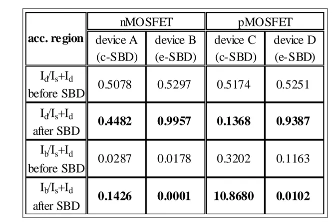
(49) nMOSFET acc. region device A device B (c-SBD) (e-SBD). pMOSFET device C device D (c-SBD) (e-SBD). Id/Is+Id before SBD. 0.5078. 0.5297. 0.5174. 0.5251. Id/Is+Id after SBD. 0.4482. 0.9957. 0.1368. 0.9387. 0.0287. 0.0178. 0.3202. 0.1163. 0.1426. 0.0001. 10.8680. 0.0102. Ib/Is+Id before SBD Ib/Is+Id after SBD. Table 3.1 The ratio of Id/(Is+Id) and Ib/(Is+Id) before and after soft breakdown in four SOI MOSFETs. The measurement is in the accumulation region and Vg= |1.5V|, Vd=Vs=0V.. 34.
(50) Current (Amp). 10. 10. 10. -5. fresh post c-SBD post e-SBD. -7. Gate current -9. Substrate current. Vd=0V. -11. 10. 0. 0.5. 1. 1.5. 2. Gate bias (volts). Fig.3.1 Gate current and substrate current versus gate bias in nMOSFETs. Solid line refers to an unstressed device and dashed line (dotted line) refers to a device after channel SBD (drain edge SBD).. 35.
(51) Body current (Amp). 10. 10. 10. -7. fresh post c-SBD post e-SBD. -9. Vg=0V. -11. 0. 0.5. 1. 1.5. 2. Drain bias (volts). Fig.3.2 Body current versus drain bias in nMOSFETs. Solid line refers to an unstressed device and dashed line (dotted line) refers to a device after channel SBD (drain edge SBD).. 36.
(52) Current (Amp). 10. 10. 10. -5. -7. Gate current -9. -11. 10. fresh post c-SBD post e-SBD. Vd=0V. Substrate current -2. -1.5. -1. -0.5. 0. Gate bias (volts). Fig.3.3. Gate current and substrate current versus gate bias in pMOSFETs. Solid line. refers to an unstressed device and dashed line (dotted line) refers to a device after channel SBD (drain edge SBD).. 37.
(53) 3.3 Modes of SBD Enhanced Hysteresis Two modes of SBD enhanced body potential alteration are proposed. Fig. 3.4 illustrates two floating-body charging processes in c-SBD and in e-SBD SOI nMOSFETs.[3.19-3.20] In a c-SBD device with a positive gate bias (Fig. 3.4(a)), valence band electron tunneling from the channel to the gate is increased after SBD. The generated holes flow to the body and raise the body potential. Fig. 3.4(b) shows the drain-induced floating-body charging in an e-SBD nMOSFET. Since the breakdown path is in the drain edge, the GIDL current increases due to a stronger band bending in the n+ drain region, thus raising the body potential at a high drain bias. On the contrary, the GIDL current does not change in a c-SBD device. Likewise, Fig. 3.5 shows two possible floating-body charging processes in pMOSFETs. Due to the above two charging processes, we conclude that the body potential of both nMOSFET and pMOSFET can be modified either during gate switching or during drain switching depending on the location of a SBD spot.. 38.
(54) +Vg. valence-band tunneling. n+. n+ (a) band-to-band current +Vd. n+. n+ (b). Fig.3.4 Illustration of two soft-breakdown enhanced floating-body charging processes in SOI nMOSFETs. (a) soft breakdown in the channel region and hole creation due to valence band electron tunneling; (b) soft breakdown in the drain region and enhanced GIDL current.. 39.
(55) -V Vg. valence-band tunneling. p+. p+ (a) band-to-band current -V Vd. p+. p+ (b). Fig.3.5. Illustration of two soft-breakdown enhanced floating-body charging processes. in SOI pMOSFETs. (a) soft breakdown in the channel region and valence band electron tunneling from poly-gate to the floating body; (b) soft breakdown in the drain region and enhanced GIDL current.. 40.
(56) 3.4 Results and Discussion Fig. 3.6 shows the Ids-Vgs hysteresis in a PD SOI nMOSFET before and after c-SBD. The measurement drain bias is 0.1V. The gate bias is swept from 0V to 1.3V and then is reversely swept from 1.3 to 0V. Note that (i) the sub-threshold hysteresis before SBD is insignificant and (ii) the post-SBD hysteresis is induced by gate bias sweep in this device. The corresponding body potential fluctuation in gate bias sweep is shown in Fig. 3.6. The arrow in the figure indicates the direction of bias sweep. After c-SBD, the body potential begins to rise when the Vg amplitude is above 0.8V. The gate switching induced body potential variation can be as large as 0.3V in this case. The pre-SBD body potential hysteresis at the same switching amplitude is less than a few tens of milli-volts. The c-SBD induced Vt hysteresis is also observed in a pMOSFET. The measurement data are not shown here. In an e-SBD device, although gate enhanced hysteresis is not observed, drain sweep induced hysteresis in sub-threshold leakage current is remarkable (Fig. 3.7). In this figure, the measurement Vgs is 0V and the drain bias is swept from 0V to 1.3V and then reversely swept back. The body potential variation is shown in Fig. 3.7, too. The e-SBD enhanced hysteresis effect is clearly shown in this figure. It should be noted these breakdown-induced hysteresis effects occurs in off-state rather than in on-state where hot carrier impact ionization has been reported as a responsible charging mechanism.[3.5] The relationship between the magnitude of sweep voltage and the body potential hysteresis in the two SBD modes is investigated. In nMOSFETs, the degree of hysteresis in terms of the body potential variation versus the amplitude of the sweep voltage is shown in Fig. 3.8 for gate bias sweep and in Fig. 3.9 for drain bias sweep. The hysteresis voltage is defined as the maximum substrate charging voltage during the sweep. In gate bias sweep (Fig. 3.8), the c-SBD device shows an increased hysteresis voltage while the hysteresis voltage of the e-SBD device is almost unchanged. In contrast, the e-SBD device shows a larger hysteresis voltage in drain bias sweep (Fig. 3.9). Similar results in pMOSFETs are presented. 41.
(57) in Fig. 3.10 for gate bias sweep and in Fig. 3.11 for drain bias sweep. From our characterization, we found SBD induced hysteresis effect may become appreciable even when the supply voltage is below 0.8V. The impact of SBD enhanced body charging effect in CMOS operation is described as follows. Fig. 3.12 illustrates the dominant Vt hysteresis modes in a SOI CMOS inverter. Hot carrier (HC) induced floating body charging occurs in on state [3.1,3.5] and it is dominant only when the inverter is during switching. On the other hand, floating body charging takes place in c-SBD (e-SBD) nMOSFETs and e-SBD (c-SBD) pMOSFETs when the input signal is at high (low) state. Since the soft breakdown induced body charging is in the off state, the time for charging can be much longer than the on-state HC caused body charging. Our study reveals that SBD in PD SOI MOSFETs not only increases leakage current but also affects circuit stability.. 3.5 Summary The significance of soft breakdown position to Vt hysteresis in PD SOI CMOS devices has been evaluated. Two SBD enhanced hysteresis modes in off-state CMOS are identified. The dominant floating body charging mechanism is valence band tunneling in c-SBD devices and band-to-band tunneling in e-SBD devices. The SBD enhanced hysteresis effect may occur even with supply voltage less than 1.0V and would be a serious reliability concern in ultra-thin oxide PD SOI circuits.. 42.
(58) 10. pre c-SBD post c-SBD. -4. 10. 0.5 0.4. Vd=0.1V. 0.3. -6. 0.2. 10. 0.1. -8. 10 10. 0. -10. 0. 0.5. 1. 1.5. Gate bias (volts). Fig.3.6 Hysteresis in Ids and corresponding floating-body potential versus Vg in a c-SBD SOI nMOSFETs. Measurement is performed with forward and then reverse drain sweeps from 0V to 1.3V.. 43. Body voltage (volts). Drain to source current (Amp). -2.
(59) 10. 0.5. -7. 10. pre e-SBD post e-SBD. 0.4. Vg=0V. 0.3 0.2. -8. 0.1. 10. 0 -9. 10. 0. 0.5. 1. 1.5. Drain bias (volts). Fig.3.7 Hysteresis in sub-threshold current and corresponding floating-body potential in an e-SBD SOI nMOSFETs. Measurement is performed with forward and then reverse drain sweeps from 0V to 1.3V.. 44. Body voltage (volts). Drain to source current (Amp). -6.
(60) Hysteresis voltage, Vb (volts). 0.5 0.4 0.3. fresh post c-SBD post e-SBD. 0.2. Vd=0V. 0.1 0 0. 0.5. 1. 1.5. Max. sweep gate bias (volts). Fig.3.8 The variation of body voltage Vb as a function of the amplitude of gate bias sweep in SOI nMOSFETs. Vd=0V.. 45.
(61) Hysteresis voltage, Vb (volts). 0.5 0.4 0.3. fresh post c-SBD post e-SBD. 0.2. Vg=0V. 0.1 0 0. 0.5. 1. 1.5. Max. sweep drain bias (volts). Fig.3.9 The variation of body voltage Vb as a function of the amplitude of drain bias sweep in SOI nMOSFETs. Vg=0V.. 46.
(62) Hysteresis voltage, Vb (volts). -0.5 fresh post c-SBD post e-SBD. -0.4 -0.3. Vd=0V. -0.2 -0.1 0 -1.5. -1. -0.5. 0. Max. sweep gate bias (volts). Fig.3.10 The variation of body voltage Vb as a function of the amplitude of gate bias sweep in SOI pMOSFETs. Vd=0V.. 47.
(63) Hysteresis voltage, Vb (volts). -0.5 fresh post c-SBD post e-SBD. -0.4 -0.3. Vg=0V. -0.2 -0.1 0 -1.5. -1. -0.5. 0. Max. sweep drain bias (volts). Fig.3.11 The variation of body voltage Vb as a function of the amplitude of drain bias sweep in SOI pMOSFETs. Vg=0V.. 48.
(64) Vcc. c-SBD. e-SBD. Vout Vin. Vout. Vin c-SBD. e-SBD GND. HC. Fig.3.12 Illustration of dominant Vt hysteresis modes in the switching of an SOI CMOS inverter.. 49.
(65) Chapter 4 Soft Breakdown Enhanced Excess Low-Frequency Noise in Ultra-Thin Oxide SOI n-MOSFETs 4.1 Introduction Silicon-on-insulator (SOI) technology also has regarded as a hopeful technology for system-on-a-chip applications, which require high-performance, low power, fully integrated RF, and mixed-signal circuits.[4.1-4.5] However, the troublesome floating-body effect (FBE) in PD SOI MOSFETs leads to kink in drain current characteristics as well as some undesirable transient effects.[4.1-4.4] FBE also gives rise to excess low-frequency noise with a Lorentzian-like spectrum in floating body PD SOI devices, posing a serious problem for base band signal processing system.[4.6-4.9] The observed Lorentzian shaped noise is caused by white thermal noise (Nyquist or shot) sources associated with the generation and removal of body charge.[4.6] The Lorentzian signature is obtained through the trans-impedances coupling these internal white noise sources to the terminals of the SOI device.[4.7] Several causes of the Lorentzian-like spectrum in SOI MOSFETs have been proposed. The origin of these floating body noises could be related to high drain bias induced impact ionization current and large gate bias induced valance band electron tunneling through the ultra-thin gate oxide.[4.9-4.10] Chapter 3 has pointed out that soft breakdown enhanced substrate tunneling current would induce threshold voltage (Vt) hysteresis effects in PD SOI MOSFETS.[4.11] The aim of this chapter is to describe the impact of soft breakdown location on the excess low-frequency noise for SOI devices with floating body configuration. In the beginning, the excess noise model in PD SOI MOSFETs is introduced. Then, the kink effect in ultra-thin oxide floating body SOI n-MOSFETs is studied, which would induce excess low frequency noise. After that, the impact of soft breakdown location on drain current noise in ultra-thin oxide SOI n-MOSFETs is investigated. In a channel breakdown device, a. 50.
(66) noise overshoot phenomenon is observed in the ohmic regime. It is characterized by a peak in current noise spectral density versus the operation gate voltage, whereby the peak amplitude can be about one order of magnitude higher than the background flicker noise. The origin of this excess noise is believed due to soft breakdown (SBD) enhanced valance-band electron tunneling and thus induced floating body effect. The findings indicate that channel SBD enhanced drain current noise can be a reliability issue in PD analog SOI CMOS circuit.. 4.2 Excess Low-Frequency Noise Model in SOI MOSFETs The major noise sources of an SOI MOSFETs operating in strong inversion are shown in Fig. 4.1. There are two noise sources associated with the conducting channel. One is flicker (1/f) noise which contributes to the low-frequency noise, the other is thermal noise which dominates at high frequency. In addition to the noise in the channel, there are two shot noise sources associated with the floating-body, which are due to the impact ionization current and the body-source diode current, respectively. In bulk MOSFET, only 1/f noise can be observed at low-frequency. However, excess noise is found in floating-body PD SOI MOSFET. The excess noise originates in the two shot noises. Although the shot noises are small in magnitude compared with flicker noise, they are amplified by FBE and give rise to the excess low-frequency noise in PD SOI MOSFET. The low-frequency noise in floating-body PD SOI MOSFET’s includes white noise, flicker noise and the FBE-induced excess noise.. A. White Noise. The white noise component originates from thermal random motion of carriers in the channel. . B. Flicker Noise. Flicker noise is a fluctuation in conductance with a power spectral density proportional to. 51.
(67) 1/fβ, where β is close to unity so that flicker is normally called 1/f noise. There is no consensus to the origin of the 1/f noise, it is very likely that there exist more than one mechanism giving rise to the same noise characteristics. According to McWhorter’s number fluctuation theory [4.12], 1/f noise is attributed to the trapping and de-trapping processes of the charges in the oxide traps close to the Si–SiO2 interface. Hooge’s empirical model [4.13], however, considers the 1/f noise as a result of carrier mobility fluctuation due to lattice scattering. It has been reported that both the carrier number fluctuation and the mobility fluctuation are possible mechanisms which lead to the 1/f noise in MOSFET’s [4.14-4.15]. Hence, for the 1/f noise, a correlated noise model [4.14] which incorporates both mechanisms is applied. S id −1/ f =. kTqI ds µ eff. γfLeff. 2. Vds. ∫. Nt (E f ). 0. N. (1 + αµ eff N ) 2 dV. where. C.. Sid-1/f. 1/f noise current spectral density;. Ids. drain current;. µeff. effective mobility;. γ. attenuation coefficient of the electron wave function in the oxide;. Leff. effective channel length of the device;. Vds. drain bias;. Nt(Ef). oxide trap concentration around the quasi-Fermi level along the channel;. N. carrier concentration along the channel;. α. lattice scattering coefficient.. Excess Low Frequency Noise. 52. (4.1).
(68) The excess low-frequency noise is specific to PD SOI MOSFET’s associated with the floating-body effect (FBE). The noise small-signal equivalent circuit shown in Fig. 4.2(a) can explain the mechanism underlying the excess low-frequency noise [4.6]. The shot noise results from the impact ionization current (Iii):. Sib1 = M ⋅ 2qI ii. (4.2). where M is a multiplication factor [4.16]. Impact ionization current exhibits shot noise because only the carriers with sufficient kinetic energy can generate electron-hole pairs. The second noise source is associated with the body-source diode current (Ibs) where carriers have to overcome the built-in potential barrier:. Sib 2 = 2qI bs. (4.3). The two noise current flow through the body-ground impedance ( ceq and req ), leading to a fluctuation in body potential:. S vb = Sib ⋅ | zb |2 = S ib ⋅ | (. = Sib ⋅. req. 1 + jωceq ) −1 |2 req. 2. (4.4). f 1 + ( )2 fc. where. Sib = Sib1 + Sib 2. and. 53. fc =. 1 2π ⋅ req ceq.
(69) The equivalent body-ground resistance req is equal to the small-signal resistance of the body-source junction. The equivalent body-ground capacitance ceq can be modeled as the sum of all the capacitance seen from the body. The schematic for req and ceq is shown in Fig. 4.2(b). And, the fluctuation in the body potential modulates the threshold voltage of the device:. Svth = Svb ⋅ (. ∂Vth 2 ) ∂Vbs. (4.5). Due to the fluctuation in Vth, the excess drain current noise is given by:. Sid −excess = S vth ⋅ (. ∂I ds 2 ) ∂Vth. ( M + 1) ⋅ 2qI ii g mb req = f 1 + ( )2 fc 2. 2. (4.6). where gmb is the body trans-conductance. The excess noise shows a Lorentzian power spectrum, which is characterized by a constant plateau at low frequency and a 1/f 2 roll-off at higher frequencies. Since white noise, 1/f noise and excess noise are uncorrelated, the total spectrum density of low-frequency drain current noise is the sum of the three components (Fig 4.3):. Sid −total = Sid −1/ f + Sid −excess + Sid − white. 54. (4.7).
(70) To verify the proposed low-frequency noise model, the noise measurement is conducted according to the setup shown in Fig. 4.4. The DC bias to the DUT is supplied by the Berkeley Technology Associate BTA9603 Noise Analyzer, which eliminates the residual noise in the bias voltages generated by HP4155C Semiconductor Parameter Analyzer. The noise current of the DUT is amplified by the low-noise amplifiers in BTA9603 before being applied to the Stanford Research SR780 Network Signal Analyzer (bandwidth: dc to 100 kHz) for FFT (fast Fourier transform). A computer installed with Noise Pro is used to automatically control the whole measurement.. 55.
(71) Gate if2 ibs. it2. 2. Source if2 :Flicker Noise. Body. iii. 2. Drain. it2 :Thermal Noise. ibs2 :Shot Noise due to body-source diode current iii2 :Shot Noise due to impact ionization current. Fig.4.1 Noise sources in an SOI MOSFET.. 56.
(72) Body Gate. ibs2. Source. req. Ceq. iii. Cjs rjs. 2. Cbb. Cbe. Drain Cjd. Ground. iii2. Cbb: body to channel depletion cap. = 2qIiiB, ibs = 2qIbsB Cjs/jd: body to S/D junction cap. Rjs: body to source AC resistance req = rjs, Ceq = Cbb + Cbe + Cjs + Cjd B: noise band width 2. (a). (b). Fig.4.2 (a) Noise small-signal equivalent circuit for the floating-body and (b) schematic for the req and Ceq network.. 57.
(73) Power 1/f noise Spectral Lorentzian Density (log) plateau 1/f 2 corner frequency white noise frequency (log). Fig.4.3 Typical input-referred low-frequency noise spectrum.. 58.
(74) BTA 9603 FET Noise Analyzer DGBS. VD VG VB VS. Device Under Test. HP 4155C Semiconductor Parameter Analyzer. Fig.4.4 Low-frequency noise measurement setup.. 59. SId. SR 780 Dynamic Signal Analyzer.
(75) 4.3 Kink Effect Induced Excess Low-Frequency Noise The SOI devices in this chapter were made with a 0.13µm standard CMOS process on p-type silicon substrate. Fig. 4.5 shows ours measured Id-Vd characteristics of SOI n-MOSFETs (W/L = 10μm/0.18μm) with floating body and grounding body. Gate is biased at 0.9V. The kink effect is obviously observed in a floating body n-MOSFET and not in an n-MOSFET with body grounded. Due to the impact ionization current, electron-hole pairs are created at the drain end. Then, the holes go to the floating body, which induce the variation of body potential. At the kink point where the body potential sufficiently increases, threshold voltage drops and thus causes an increase of the drain current. The phenomenon in the floating body n-MOSFET consists with others results in PD SOI MOSFETs.[4.6] The excess noise is also found in floating body PD SOI MOSFET as the drain bias is above the kink voltage. In Fig. 4.6, normalized noise power spectrum density in an n-MOSFET with body floated is measured at gate biased 0.9 V, and drain biased 0.5V、1.0V、1.2V、1.3V、1.4V、 1.6V. Fig. 4.6 shows that the excess noise is not observable in the curve corresponding to the linear regime operation. As drain biases is above the kink onset voltage, the normalized noise power spectrum exhibits a plateau up to the characteristic frequency fc = 1/( 2π ⋅ req ceq ) before a 1/f2 roll-ff sets in. Furthermore, a typical Lorentzian shift to lower plateau and higher cut-off frequency is observed due to the increase of impact ionization current with the drain bias. Because the req decreases with increasing drain voltage, a larger drain bias gives rise to a higher fc but a smaller noise magnitude. Additionally, Fig. 4.7 shows that normalized noise power spectrum density in an n-MOSFET with body grounded. Fig. 4.7 manifests that only flicker noise is exhibited at drain biased from linear regime to saturation regime. That is, the excess noise can be effectively eliminated, as body contact is grounded. Fig. 4.8 illustrates that the normalized drain current noise initially increases with the drain voltage and reaches a peak when the kink. 60.
(76) point appears for a given frequency. This is when the device switches from linear operation regime to the regime around the kink point with the increase of the drain voltage. The low-frequency noise in floating-body PD SOI MOSFETs is composed of 1/f noise and shot noise-induced excess noise. High drain bias gives rise to impact ionization current which flows through the floating-body to the source terminal. The shot noise causes fluctuation of body potential and threshold voltage, and consequently leads to excess noise in drain current. The RC network of the body in floating-body PD SOI MOSFETs amplifies and filters the shot noise, giving rise to a Lorentzian-like spectral density in noise. The noise peaks around the kink onset voltage for a given frequency. These experimental results consisted with previous mentioned noise model.. 61.
(77) -4. 6.0x10. Id (Amp). -4. 4.0x10. W/L=10µm / 0.18µm Vg=0.9V. -4. 2.0x10. Vb=0V Vb=floating. 0.0 0.0. 0.5. 1.0. 1.5. Vd (volts). Fig.4.5 The Id-Vd characteristics in nMOS SOI devices with floating body and grounding body when gate is biased at 0.9V.. 62.
(78) -9. 10. Vg=0.9V Vb=floating. Vd=0.5V. SId/Id (1/Hz). Vd=1.0V Vd=1.2V -11. Vd=1.3V. 10. Vd=1.4V. 2. Vd=1.6V -13. 10. -15. 10. 0. 10. 1. 10. 2. 3. 10. 10. 4. 10. 5. 10. frequency (Hz). Fig.4.6 Normalization noise power spectral density in floating body nMOS SOI devices under different drain voltage when gate is biased at 0.9V.. 63. 6. 10.
(79) -9. Vg=0.9V Vb=0V Vd=0.5V Vd=1.0V. -11. 10. Vd=1.2V Vd=1.4V. 2. SId/Id (1/Hz). 10. Vd=1.6V -13. 10. -15. 10. 0. 10. 1. 10. 2. 3. 10. 10. 4. 10. 5. 10. 6. 10. frequency (Hz). Fig.4.7 Normalization noise power spectral density in grounding body nMOS SOI devices under different drain voltage when gate is biased at 0.9V.. 64.
(80) -10. -11. float @100Hz bulk @100Hz float @1KHz bulk @1KHz. 10. 2. SId/Id (1/Hz). 10. -12. 10. -13. 10. 0.4. 0.6. 0.8. 1.0. 1.2. 1.4. 1.6. Vd (volts). Fig.4.8 Comparison of normalization noise power spectral density under different drain bias in floating body SOI devices and grounding body SOI devices for given frequency.. 65.
數據
相關文件
Search the portion of List preceding TestEntry for TargetValue, and report the result of that search if (TargetValue > TestEntry):. Search the portion of List following
細目之砂紙,將絕緣體 及內部半導電層鉛筆狀
Z 指令 ping 為重要的使用 ICMP 封包的指令. Z 若設定防火牆,並非所有的 ICMP
• 後段工程是從由矽晶圓切割成一個一個的晶片 入手,進行裝片、固定、接合連接、注模成 形、引出接腳、按印檢查等工序,完成作為元
然而,目前探討職務再設計如何協助中高齡工作者老化的議題時,通常
◦ 金屬介電層 (inter-metal dielectric, IMD) 是介於兩 個金屬層中間,就像兩個導電的金屬或是兩條鄰 近的金屬線之間的絕緣薄膜,並以階梯覆蓋 (step
決定隱藏層神經元數,對一層隱藏層觀察神經元數 1~10 個之測試 範例誤差均方根 RMS 最小者,結果取隱藏層觀察神經元數為 10
李友錚【5】指出有關顧客需求特性的探討目前以 Kano 二維品質模式 最具代表。因此,可以利用 Kano
