國
立
交
通
大
學
電子工程學系 電子研究所
博 士 論 文
高壓製程積體電路之
靜電放電防護設計與應用
Design and Applications of ESD Protection
in High-Voltage Integrated Circuits
研 究 生:陳穩義
指導教授:柯明道 教授
高壓製程積體電路之
靜電放電防護設計與應用
Design and Applications of ESD Protection
in High-Voltage Integrated Circuits
研 究 生:陳穩義 Student:Wen-Yi Chen
指導教授:柯明道 Advisor:Ming-Dou Ker
國 立 交 通 大 學
電子工程學系 電子研究所
博 士 論 文
A DissertationSubmitted to Department of Electronics Engineering and Institute of Electronics
College of Electrical and Computer Engineering National Chiao Tung University
in partial Fulfillment of the Requirements for the Degree of
Doctor of Philosophy in
Electronics Engineering Dec. 2011
Hsinchu, Taiwan, Republic of China
高壓製程積體電路之靜電放電防護設計與應用
研究生:陳穩義
指導教授:柯明道 博士
國立交通大學電子工程學系電子研究所
摘要
高壓製程積體電路在車用電子,消費性電子產品,以及驅動電路等方面,
近年來均獲得極大的重視與廣泛應用。在電子系統中,靜電放電防護能力
為產品可靠度的重要指標之一。在高壓製程中,由於複雜的元件結構,其
靜電放電防護設計,具有相當之困難度及挑戰。
N 型橫向雙擴散金氧半電晶體 (n-channel lateral DMOS)普遍具有不佳
之靜電放電防護能力;為了提升該元件之靜電放電防護能力,一具格子形
狀 (waffle)之特殊佈局方式於章節二中提出。該佈局方式可使元件保存其電
流驅動能力,並於對角線上得到額外之觸發點;透過該額外觸發點,N 型
橫向雙擴散金氧半電晶體得以透過基極觸發之技巧,來促進靜電放電發生
時,元件之均勻導通程度,以提升其靜電放電防護能力。該佈局成效已於
一
0.5 微米及一 0.35 微米高壓製程中獲得實際驗證。
使用矽控整流器為在高壓製程中提升靜電放電防護能力的解決方案之
一。然而,矽控整流器在實際應用中,會造成其他可靠度疑慮,例如元件
之安全操作區間(Safe Operating Area)受到壓縮。在章節三中,首先針對安
全操作區間及目前習知的改進技術,做一詳細的介紹。於章節四中,則特
別提出一多晶矽閘極彎曲之特殊元件佈局方式,以改善因使用矽控整流器
在
N 型橫向雙擴散金氧半電晶體中,對安全操作區間所造成的負面影響。
除兩種元件等級的新型佈局方式外,由於積體電路產品需要達到靜電放
電防護能力的規格要求,本論文分別於章節五及章節六,提出兩個已成功
應用於商用積體電路產品的創新靜電放電防護設計。此兩個靜電放電防護
設計,皆應用於全金屬矽化物製程(fully-silicided)之積體電路產品。使用全
金屬矽化物製程可提升積體電路產品的電路性能,但卻會造成靜電放電防
護能力的下降。特殊的靜電放電防護設計,為全金屬矽化物製程中的必要
設計。章節五中,透過兩種鎮流電阻(ballast resistance)設計方式,順利將一
款微控制積體電路晶片之人體靜電放電模式靜電放電防護能力,由
1.5 千
伏特提升至超過
6 千伏特。
章節六的全金屬矽化物製程靜電放電防護設計,為專為電壓程式腳位應
用所做出的創新設計。在記憶體寫入時,該電壓程式腳位將升壓至一大於
正常工作電壓之電位。因此,該腳位之靜電放電防護設計,需符合開汲極
與故障保險(open drain / fail safe)的設計需求:自電壓程式腳位至電源線間,
不能有順偏二極體的存在,以避免漏電流的產生。此外,該靜電放電防護
設計,在電壓程式訊號具備極快速的電壓上升時間(數十奈秒等級)下,仍可
避免誤觸發的問題,不影響記憶體寫入的操作。此一特性,使得具備該靜
電放電防護設計的微控制器,可通用市面上多種記憶體寫入器。本靜電放
電防護設計,已於一矽晶片上實際驗證,可提供五千伏特之人體靜電放電
防護耐受度。
在廣泛的可靠度議題中,除靜電放電防護設計外,閂鎖效應為另一個重
要的設計考量。在考量閂鎖效應時,元件之維持電壓(holding voltage)為一
重要的參考指標。章節七則探討
N 型橫向雙擴散金氧半電晶體,其維持電
壓對時間的關聯性。透過長脈寬傳輸線觸波產生系統的量測,發現
N 型橫
向雙擴散金氧半電晶體的維持電壓,會隨著時間的經過而下降。該現象將
造成未來高壓製程中閂鎖效應的測試方式與佈局準則訂定的不同考量。
簡而言之,本論文提出創新的學術研究貢獻,更針對實際積體電路產品
之靜電放電防護,做出切題且創新的實用設計。本論文促進了解高壓製程
中元件於靜電放電時的反應與現象,並提供數種於高壓積體電路製程中可
實用的靜電放電防護解決方案。
DESIGN AND APPLICATIONS OF ESD PROTECTION IN
HIGH-VOLTAGE INTEGRATED CIRCUITS
Student: Wen-Yi Chen Advisor: Dr. Ming-Dou Ker
Department of Electronics Engineering, Institute of Electronics
National Chiao Tung University
Abstract
High-voltage (HV) technologies are booming in recent years due to the increasing demand on automotive electronics, consumer integrated circuits (ICs), driver circuits for display panels and so forth. To have a rigorous end product or electronic system, electrostatic discharge (ESD) is one of the most important factors affecting IC reliabilities; IC industries are struggling for good ESD protection designs due to the structural complexity of transistors and application varieties in HV technologies.
The n-channel lateral DMOS (nLDMOS) devices in HV technologies are known to have poor ESD robustness. To improve the ESD robustness of nLDMOS, a co-design method combining a new waffle layout structure and a trigger circuit is proposed in chapter 2 to fulfill the body current injection technique. The proposed layout and circuit co-design method on high-voltage nLDMOS has been successfully verified in a 0.5-m 16-V BCD process and a 0.35-m 24-V BCD process without using additional process modification. Experimental results have shown significantly improved turn-on uniformity and ESD robustness of nLDMOS.
Silicon controlled rectifier (SCR) in HV technologies is usually embedded in output arrays to provide a robust and self-protected ESD capability. Though the embedded SCR has
been proven as an excellent approach to increasing ESD robustness, mis-triggering of the embedded SCR during normal circuit operating conditions can bring other application reliability concerns. The safe operating area (SOA) of output arrays due to SCR insertion has seldom been evaluated. In chapter 3, SOA is first reviewed and in chapter 4, the impact of embedding SCR to the electrical SOA (eSOA) of an nLDMOS array is investigated. Experimental results showed the nLDMOS array suffers substantial degradation on eSOA due to the embedded SCR. Design approaches, including a new proposed poly bending layout, is proposed in chapter 4. With the poly bending layout method, both high ESD robustness and a wide SOA can be achieved at the same time on an nLDMOS output array.
In addition to the two layout designs in Chapter 2 and 4, another two practical fully-silicided designs have been applied to IC products and have passed product-level ESD verifications. Silicidation is a common process step which can improve the circuit operating speed but has been reported to substantially decrease ESD robustness of MOSFETs. Silicide blocking is a useful method to alleviate this ESD degradation from silicidation, but it requires additional mask and process steps and the fabrication cost is increased. For cost reduction, two new ballasting layout schemes are included in chapter 5 to effectively improve ESD robustness of fully-silicided push-pull I/O buffers without using the silicide blocking. Results from real IC products have confirmed that the new ballasting layout schemes can successfully increase human-body model (HBM) ESD robustness of fully-silicided I/O buffers from 1.5 to over 6 kV.
The other fully-silicided ESD protection design in chapter 6 is for ICs with a voltage programming (VPP) pin. When programming read only memories (ROM), a voltage higher
than the normal power supply voltage (VDD) is applied to the VPP pin. A fail-safe structure
that does not have a diode current path to VDD power supply line is necessary for a VPP pin. A
new VPP pin ESD protection design is necessary for the fully-silicided and the fail-safe
features high resistivity to mis-triggering when the VPP programming voltage has a fast rise
time. This special design consideration makes ICs with the ESD protection design be compatible to ROM programmers that can have fast voltage slew rate on VPP pins when
programming. This new VPP pin ESD protection design has been successfully verified on a
commercial IC product and equipped the IC with an HBM ESD protection level of 5 kV. Besides the requirement of high ESD robustness, latchup is another important reliability consideration for silicon ICs, especially in HV technologies. Holding voltage is one of the critical design considerations when developing elements with high latchup immunity. Because a HV device is easily damaged by the huge power generated from direct current (DC) curve tracer, the device holding voltage with respect to latchup immunity is often referred to the holding voltage measured by TLP systems with a 100-ns pulse width. To evaluate the validity of this practice, a long-pulse TLP system were used to investigate characteristics of an nLDMOS’s holding voltage in time domain. Measurement results in chapter 7 revealed that the self-heating effect results in overestimation of the holding voltage acquired from a 100-ns TLP system. A gradually decreasing holding voltage of the nLDMOS in time domain is observed, which leads to new concerns when engineering holding voltage of transistors in HV technologies. With these novel results in HV technologies, this dissertation provides both advanced academia research achievements and practical ESD design solutions to IC industries.
Acknowledgment
在報考博士班前,曾經有前輩在鼓勵之餘也告訴我,博士班是一條漫長
而孤獨的道路。從打開這扇門起跑開始,到撰寫這篇致謝準備朝向接下來
的目標前進;回首這段時間的歷程,不自覺令人想起這句感觸良多的話語。
在這條路上,我想我是幸運的;因為不論在學業或精神上,我都得到許多
來自師長、同儕或家人的支持,讓我得以順利完成博士學業。
來自家人的陪伴與支持,一直是我在感到無助和徬徨時最大的精神支
柱。我要向我的父親陳世霖先生,以及母親林清珠女士,獻上最崇高的感
謝與敬意。由於有您們對我從小無怨的付出,以及一路給我的關心和栽培,
才讓我的人生得以有諸多的選擇,並完成我的博士學業。希望在不久的將
來,我能開始回報您們的恩情。我也要感謝我的太太陳瑩柳女士;由於妳
的存在與陪伴,增添了這條孤獨道路上的溫暖。同時,也感謝我的哥哥陳
瑞宗先生、嫂嫂林易汶女士,您們所帶給我屬於家人的親情,是一種無可
取代的聯繫與鼓勵。
在學業上,我要特別感謝我的指導教授柯明道博士,在論文以及研究上
的指導,及研究資源上的提供,讓我得以順利完成我的研究,並撰寫成博
士論文。在交大曾經指導我的學長們、在實驗室一起熬夜的同學們、一直
給我鼓勵及幫助的業界學長們、以及一起完成計劃的學弟妹們:陳東暘博
士、徐國鈞博士、林昆賢博士、許勝福博士、張瑋仁博士、陳世倫博士、
蕭淵文博士、陳世宏博士、顏承正博士、陳榮昇博士、王暢資博士、林群
祐博士、王資閔博士、王文傑博士、彭政傑學長、莊哲豪學長、張智毅學
長、徐中玓學長、邱柏硯準博士(下一個換你了,加油!)、卓慧貞女士、黃
士豪、陸亭州、葉致廷、賴泰祥、黃曄仁、莊介堯、許哲綸、黃筱晴、蔡
惠雯、林倍如…等,也感謝您們在這條路上,帶給我的成長及回憶。同時,
也感謝晶焱科技的姜信欽博士、鄭俊一博士、曾當貴、林明芳、蔡耀城、
吳文政、陳子平、李健銘及吳偉琳,在甫進入博士班時,所給我的幫助。
此外,閎康科技的謝詠芬博士、朱志勳博士在故障分析知識上的專業傳承,
也對我的學業起了很大的助力。還有許多在這條路上曾經幫助過我的前輩
及朋友們,不及一一詳列,謹此表達我的謝意。
I would also like to express my most sincere gratitude to Professor Elyse
Rosenbaum, and to my friends at UIUC as well, Dr. Nicholas Olson, Nathan
Jack, Arjun Kripanidhi, Vrashank Shukla, Adam Faust, Min-Sun Keel,
Kuo-Hsuan Meng, Nick Thomson, and Robert Mertens. With your help I had a
wonderful time at U of I, and most importantly I learned different ways of
thinking and saw skills that I am short of. My experience at U of I really
broadened my horizons and urged me to set up goals for my personal growing.
Many thanks to all of you and please have my best wishes. I hope to have the
opportunity to meet you all again in the future.
陳 穩 義
謹誌於臺灣・新竹
中華民國
100 年 12 月
William Wen-Yi Chen
in Hsinchu, Taiwan
December, 2011
Contents
Abstract (Chinese)
i
Abstract (English)
iii
Acknowledgement
vi
Contents
viii
Table Captions
xi
Figure Captions
xii
1. Introduction 1
1.1. High-Voltage Technologies in Integrated Circuits 1
1.2. ESD and Its Design Challenges in High-Voltage Technologies 2
1.3. Dissertation Organization 6
2. Waffle Layout Structure With Body-Injected Technology in BCD
High-Voltage Processes 8
2.1. Background 8
2.2. Effect of P-type Boron Implantation on ESD Performance of High-Voltage nLDMOS 9
2.3. New Waffle Layout Structure for ESD Improvement 14
2.3.1. In the 0.5-m 16-V BCD Process 16
2.3.2. In the 0.35-m 24-V BCD Process 19
2.4. Summary 28
3. Overview to the SOA Characterization and Improvement Techniques in
Power MOSFETs 29
3.1. Background 29
3.2. Physical Limitation of SOA 29
3.3. Switching Reactive Loads 34
3.3.2. Inductive Load (Unclamped Inductive Switching) 36
3.3.3. Inductive Load (Clamped Inductive Switching) 40
3.4. Techniques to SOA Improvement 42
3.4.1. Additional Body Implantation 42
3.4.2. Dotted Channel LDMOS 44
3.4.3. Drift Configurations 45
3.4.4. Thick Copper Metallization 46
3.4.5. Power Distribution 47
3.5. Summary 48
4. High-Voltage Output Arrays and The Poly-Bending Layout for the
eSOA Improvement of SCR-nLDMOS 49
4.1. Background 49
4.2. Test Structures of HV nLDMOS 50
4.3. Electrical SOA of nLDMOS and SCR-nLDMOS Arrays 52
4.3.1. PBI Layer to eSOA of nLDMOS 52
4.3.2. SCR-nLDMOS and DP width to eSOA (GateSCR internally short circuited to GateMOS) 54
4.3.3. GateSCR bias to eSOA of SCR-nLDMOS (ggSCR-nLDMOS) 60
4.4. Poly Bending Structure to SCR-nLDMOS 62
4.5. Summary 67
5. New Ballasting Layout Schemes to Improve ESD Robustness of I/O
Buffers in Fully-Silicided CMOS Processes 68
5.1. Background 68
5.2. Review on Ballasting Techniques for Fully-Silicided I/O Buffers 69
5.3. Fully-Silicided I/O Buffers under ESD Stresses 74
5.3.1. Fully-Silicided I/O Buffer Without Ballasting 76
5.3.2. I/O Buffer with N-Well Ballasting on Driver NMOS 78
5.4. New Layout Schemes for Fully-Silicided I/O Buffers 82
5.4.1. I/O Buffer with The New Proposed Layout Scheme (Type A) 83
5.4.2. I/O Buffer with The New Proposed Layout Scheme (Type B) 86
6. Fully-Silicided ESD Protection Design on The Voltage Programming
Pins of ICs with One-Time Programming Memories 92
6.1. Background 92
6.2. Design Considerations of Voltage Programming Pins 94
6.2.1. OTP Memory Cells 94
6.2.2. VPP Programming Waveforms 94
6.2.3. Previous ESD Protection Designs for VPP Pins 98
6.3. New Proposed VPP ESD Protection Design 99
6.4. Implementation and ESD Testing Results 103
6.4.1. Ballast Layout to Fully-Silicided High-Voltage NMOS 103
6.4.2. ESD Discharging Paths 105
6.4.3. ESD Measurement Results 107
6.5. Summary 110
7. Investigation on The Transistor Holding Voltage Acquired from TLP in
a High-Voltage Technology 112
7.1. Background 112
7.2. Device Structure 113
7.3. Experimental Results and Discussion 113
7.4. Summary 117
8. Conclusions and Future Works 118
8.1 Main Results of This Dissertation 118
8.2 Future Works 119
References
121
Vita
136
Table Captions
Chapter 2.
Table 2.1. ESD robustness of nLDMOS devices 28
Chapter 5.
Table 5.1. ESD robustness among the I/O buffers 77
Chapter 6.
Table 6.1. Device dimensions of the ESD protection design 101 Table 6.2. Measured HBM ESD robustness of the IC product with previous ESD protection design or the proposed ESD protection design at VPP pin. 108
Figure Captions
Chapter 1.
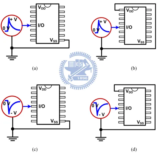
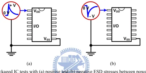
Fig. 1.1. Equivalent circuits of (a) HBM and (b) MM ESD tests. 2 Fig. 1.2. A complete ESD protection network for general CMOS ICs. 2 Fig. 1.3. Packaged IC tests at I/O pins with (a) positive-to-VSS (PS-), (b)
positive-to-VDD (PD-), (c) negative-to-VSS (NS-), and (d) negative-to-VDD
(ND-), mode ESD stresses. 3 Fig. 1.4. Packaged IC tests with (a) positive and (b) negative ESD stresses between power pins. 4 Fig. 1.5. Measured MM ESD protection levels of nLDMOS with different effective channel widths. 5 Fig. 1.6. ESD current discharging path in an open drain structure. Without a
forward diode from the pad to the HV VCC power supply line, power-rail
ESD clamp circuit does not help discharge ESD current. 5
Chapter 2.
Fig. 2.1. (a) Layout diagram and the (b) device cross-sectional view along A-A’ line of the nLDMOS in a 0.5-m 16-V BCD process with the optional PBI layer. 9 Fig. 2.2. (a) Layout diagram and the (b) device cross-sectional view along A-A’ line of the nLDMOS in a 0.35-m 24-V BCD process. 10 Fig. 2.3. TLP-measured I-V characteristics of the gate-grounded 16-V nLDMOS
devices with or without the PBI layer. 11 Fig. 2.4. The typical I-V characteristic of a gate-grounded NMOS under ESD stresses. 13 Fig. 2.5. (a) Layout top view, (b) device cross-sectional view along A-A’ line, and (c) device cross-sectional view along B-B’ line, of the nLDMOS with the proposed waffle layout style in the 0.5-m 16-V BCD process. 15
Fig. 2.6. Turn-on verification of the stand-alone 16-V nLDMOS drawn in waffle style with DC body current (IB) injected from the trigger nodes. 17
Fig. 2.7. Turn-on verification of the stand-alone trigger circuit in the 0.5-m 16-V BCD process. The measurement setup is shown in the inset of this figure. 17 Fig. 2.8. The 100-ns TLP-measured I-V curves of 16-V nLDMOS with stripe,
waffle, and body-injected waffle layout style. 18 Fig. 2.9. Scanning electron microscope (SEM) image of the body-injected waffle nLDMOS after 100-ns TLP measurement. 19 Fig. 2.10. TLP-measured I-V characteristics of stand-alone 24-V nLDMOS in stripe layout style. Dimension for each finger of the stripe nLDMOS is 73.2 m/0.75 m. 20 Fig. 2.11. TLP-measured I-V characteristics of stand-alone 24-V nLDMOS in waffle layout style. Dimension for each drain square of the waffle nLDMOS is 73.2 m/0.75 m. 20 Fig. 2.12. (a) SEM image of the stand-alone 24-V waffle nLDMOS with 22 drain squares after 100-ns TLP measurement and (b) the enlarged image of ESD failure locations. 21 Fig. 2.13. Turn-on verification of the stand-alone trigger circuit in the 0.35-m 24-V BCD process. The measurement setup is shown in the inset of this figure. 22 Fig. 2.14. TLP-measured I-V characteristics of body-injected 24-V nLDMOS with waffle layout style. 23 Fig. 2.15. Layout diagram of the 24-V stripe nLDMOS with additional P+ trigger bars at upper and bottom of the device for body current injection. 23 Fig. 2.16. TLP-measured I-V characteristics of body-injected 24-V nLDMOS in stripe layout style. 24 Fig. 2.17. Normalized It2 current among different types and fingers of 24-V
nLDMOS. 25 Fig. 2.18. SEM image of the body-injected 24-V nLDMOS with stripe layout style after 100-ns TLP measurement. 26
Fig. 2.19. OBIRCH and SEM images of the body-injected 24-V nLDMOS with waffle layout style after 100-ns TLP measurement. 27
Chapter 3.
Fig. 3.1. Design triangle of power semiconductor devices (redrawn after [32]). 29 Fig. 3.2. The equivalent circuit model of a HV NMOS. Parasitic BJT and resistors are included. 30 Fig. 3.3. Test setup of eSOA measurement with 100-ns TLP. 30 Fig. 3.4. Measured eSOA boundaries of two nLDMOS transistors. 31 Fig. 3.5. A diagram showing tendencies of eSOA and tSOA with respect to temperature and pulse widths. 32 Fig. 3.6. A Diagram showing FB-SOA of a power MOSFET. 33 Fig. 3.7. Test circuit of an nLDMOS switching an external capacitor. CEXT with
different capacitances were used in this test. 34 Fig. 3.8. Measured (a) turn-on waveforms and (b) I-V trajectories of an nLDMOS switching capacitors with different capacitance values. 35 Fig. 3.9. Test circuit for unclamped inductive switching of an nLDMOS. 36 Fig. 3.10. Measured UIS waveforms with different LEXT, VCC, or TPW parameters. (a)
LEXT = 220 H, VCC = 24 V, TPW = 1 s, (b) LEXT = 220 H, VCC = 12 V,
TPW = 1 s, (c) LEXT = 220 H, VCC = 24 V, TPW = 2 s, and (d) LEXT = 1
mH, VCC = 24 V, TPW = 4.45 s. 37
Fig. 3.11. A diagram depicting the I-V characteristic of a gate-grounded nLDMOS. 39 Fig. 3.12. A CIS test circuit using a zener diode to clamp the nLDMOS drain voltage during inductive turnoff. 40 Fig. 3.13. Measured I-V waveforms of the CIS test circuit. The breakdown voltage
of the zener diode is 37 V. 40 Fig. 3.14. Measurement setups for (a) voltage and (b) current rectangular power
pulsing test circuits (redrawn after [48]). 42 Fig. 3.15. Device cross-sections of (a) a regular nLDMOS and (b) an nLDMOS with
additional P-type implantation at body to improve SOA. 43 Fig. 3.16. Layout and device cross-sectional views of (a) a regular LDMOS and (b)
a dotted-channel LDMOS for SOA improvement (redrawn after [52]). 44 Fig. 3.17. Illustration of power MOSFET arrays with (a) single step, (b) dual step, and (c) checkerboard, layout design for improving the uniformity of power distribution (redrawn after [69]). 46
Chapter 4.
Fig. 4.1. (a) Layout top view and (b) device cross-sectional view along A-A’ line of an nLDMOS without embedded SCR. 50 Fig. 4.2. (a) Layout top view and (b) device cross-sectional view along B-B’-C-C’
region of an nLDMOS with embedded SCR. 51 Fig. 4.3. Measured eSOA of nLDMOS with and without PBI layer. DUTs with IDS
from low to high were measured under gate biases of 0, 3, 6, 9, 12, and 16V. 53 Fig. 4.4. The equivalent circuit of the embedded SCR in the nLDMOS arrays. 54 Fig. 4.5. Measured TLP I-V characteristics of SCR-nLDMOS (a) without PBI and (b) with PBI. Gate bias for all DUTs was 0 V and leakage currents were measured under 24-V drain bias. 56 Fig. 4.6. Measured eSOA of SCR-nLDMOS with GateSCR short circuited to
GateMOS. The corresponding gate biases for the IDS from low to high were
0, 3, 6, 9, 12, and 16 V, respectively. Some measured DUTs have less than 6 data points because these DUTs under high gate biases were driven directly into SCR operation without manifesting distinct snapback to determine their eSOA boundaries. 57 Fig. 4.7. Measured voltage waveforms when switching a 50- resistive load under
24-V power supply voltage and a 0-to-6 V voltage pulse on gate. DUTs are (a) nLDMOS without embedded SCR and (b) SCR-nLDMOS with DP
of 50 m. Both measured DUTs do not have the PBI layer. GateSCR in the
Fig. 4.8. Measured eSOA of ggSCR-nLDMOS (GateSCR internally short to
source/body). The corresponding gate biases for the IDS from low to high
were 0, 3, 6, 9, 12, and 16 V, respectively. 61 Fig. 4.9. (a) Layout top view and (b) cross-sectional view along D-D’ line of SCR-nLDMOS with the proposed poly bending structure. Widths and spacings in figures are not drawn to scale. 63 Fig. 4.10. Performance of poly bending structure on eSOA of SCR-nLDMOS. The “PB” devices have poly bending structure with GateSCR internally
connected to GateMOS. The “PB & gg” devices have poly bending
structure with GateSCR internally connected to source/body. The
corresponding gate biases for the IDS from low to high were 0, 3, 6, 9, 12, and 16 V, respectively. 65 Fig. 4.11. Measured TLP I-V characteristics of poly bending SCR-nLDMOS with different S spacings. Gate bias for all DUTs was 0 V and the leakage currents were monitored under 24-V drain bias. 66
Chapter 5.
Fig. 5.1. Current-voltage (I-V) characteristics of gate-grounded NMOS for ESD protection, indicating the relation between Vt2 and Vt1 values to the
uniform or non-uniform triggering. 70 Fig. 5.2. Ballast N-Well to increase the ballast resistance of NMOS. The separated
diffusion region that connects to I/O Pad is labeled as island diffusion, and the diffusion region that closer to the gate is labeled as drain diffusion. 71 Fig. 5.3. The (a) layout top view and (b) device cross-sectional view along A-A’ line of the fully-silicided NMOS with floating poly array (FPA) technique [107]. 74 Fig. 5.4. Whole-chip ESD protection scheme and the corresponding device dimensions of the power-rail ESD clamp circuit. 75 Fig. 5.5. Layout top view of the self-protected fully-silicided I/O buffer in a CMOS IC product. 76
Fig. 5.6. SEM image of the fully-silicided I/O buffer without ballasting after 2-kV PS-mode ESD stress. ESD failure is found on only one finger of the driver NMOS. Current filamentation is also observed on the surface of the driver NMOS without ballasting. 78 Fig. 5.7. Diagram to show the metal connection to the I/O pad for the driver NMOS with ballast N-Well but the driver PMOS without ballasting. 80 Fig. 5.8. SEM image of the fully-silicided I/O buffer with N-Well ballasting
technique on the driver NMOS after 4.5-kV ND-mode ESD stress. Failure locations are found on the driver PMOS due to the triggering of parasitic BJT in PMOS. 81 Fig. 5.9. Diagram to show the metal connection to the I/O pad for the driver
NMOS realized with type-A layout scheme. 82 Fig. 5.10. Cross-sectional view along A-A’ line of the fully-silicided I/O buffer realized with the type-A layout scheme. 82 Fig. 5.11. TLP-measured I-V curves for the I/O buffer with the type-A layout scheme. The tests were manually stopped at 2 A without causing failure to the I/O buffer. 84 Fig. 5.12. SEM image of the fully-silicided I/O buffer realized with the type-A
layout scheme after 6.5-kV PS-mode ESD stress. Uniformly distributed N+-to-N-Well ESD damages are found on the driver NMOS. 85 Fig. 5.13. Diagram to show the metal connection to the I/O pad for driver NMOS and PMOS in the type-B layout scheme. 87 Fig. 5.14. Cross-sectional view along A-A’ line of the fully-silicided I/O buffer realized with the type-B layout scheme. 88 Fig. 5.15. TLP-measured I-V curves for the I/O buffer with the type-B layout scheme. The tests were manually stopped at 2 A without causing failure to the I/O buffer. 89 Fig. 5.16. (a) EMMI and (b) SEM images of the fully-silicided I/O buffer realized
Chapter 6.
Fig. 6.1. (a) Normal operating condition of the memory unit before programmed. Channel can be induced under VGS of 5 V and VDS of 5 V. (b) Bias
conditions of the memory unit during programming. A high control gate bias of 12.5 V is used to draw channel hot electrons into the floating gate. (c) Normal operating condition of the memory unit after programmed. Channel cannot be induced under VGS of 5 V and VDS of 5 V due to the
trapped electrons in the floating gate. 93 Fig. 6.2. Measured voltage waveforms on VD D and VP P pins during
programming. 95 Fig. 6.3. Traditional whole-chip ESD protection scheme with the power-rail ESD clamp circuit. The diode DU results in an unwanted leakage current path
when I/O voltage is higher than the VDD voltage during some special
circuit operating conditions. 96 Fig. 6.4. Previous ESD protection design for VPP pin. It can be safely programmed
with fast VPP voltage rise time but has a lower ESD protection level of
only 2 kV in HBM. 97 Fig. 6.5. SEM image of the previous ESD protection design after 2.5-kV PS-mode ESD test. ESD failure locations were found on both the FOD device and the diode DN. 98
Fig. 6.6. The proposed ESD protection design for VPP programming pin. 100
Fig. 6.7. Layout top view of the proposed ESD protection design for VPP pin,
which was realized in a 0.35-m fully-silicided CMOS process. 100 Fig. 6.8. Measured voltage waveforms on VPP pin during programming with (a)
slow TR,VPP of 2 s and (b) fast TR,VPP of 25 ns. VDD was biased at 5 V
during the tests. 102 Fig. 6.9. (a) Device cross-sectional view and (b) layout top view of the
high-voltage ESD protection NMOS (MN2) with P+ trigger node and the
N-Well ballast layout realized in a fully-silicided CMOS process. 104 Fig. 6.10. ESD current discharging paths under (a) NS-, (b) ND-, (c) PS-, and (d) PD- mode, ESD tests. The dashed lines denote the substrate-triggered
current to trigger on the ESD protection device MN2 and the solid lines
show the primary ESD current flow. 106 Fig. 6.11. TLP-measured I-V characteristics of the proposed ESD protection design
under PS-mode ESD stress. 108 Fig. 6.12. Die photograph of the IC with proposed ESD protection design at VPP pin.
Technology node used in this work is a 0.35-m fully-silicided CMOS process with OTP memory cells. 109 Fig. 6.13. (a) OBIRCH and (b) SEM images of the VPP pin with the proposed ESD
protection design after 5.5-kV PD-mode HBM ESD stress. 110
Chapter 7.
Fig. 7.1. Device cross-sectional view of the nLDMOS in an 18 V BCD process. 113 Fig. 7.2. I-V characteristics of the nLDMOS measured by (a) 100-ns and 1000-ns TLP, and (b) a DC curve tracer. 114 Fig. 7.3. Time-domain waveforms of the nLDMOS under 1000-ns long-pulse TLP measurement. 115 Fig. 7.4. Time-domain voltage waveform of the nLDMOS under transient latchup measurement with initial positive Vcharge of +30V. 116
Chapter 1
Introduction
In this chapter, the role and applications of high-voltage (HV) technologies in integrated circuits (ICs) are introduced. Test methods and standards of electrostatic discharge (ESD) related to this dissertation are reviewed as well. Followed by the dissertation organization, this chapter provides motivation and staring materials to the research results of this dissertation.
1.1. High-Voltage Technologies in Integrated Circuits
With the thriving applications in consumer electronics, automotive electronics, display driver and power management ICs…etc., HV technologies are booming in recent years. Due to different application-oriented considerations, HV technologies have a wide spectrum of power levels and can mainly be classified in three categories [1]. The first category has a wide operating voltage (from several tens of volts up to 300 V) but low operating current. Examples for this category include plasma display panel (PDP), light-emitting diode (LED), and liquid crystal display (LCD) driver ICs. A cost-effective solution is usually the development target of this category. The second category has a relatively low (< 100 V) operating voltage. Examples for this category include automotive electronics and power management ICs for computers. Low turn-on resistance, fast switching speed and robust operating characteristics are requirements for this category. The third category has a relatively high blocking voltage (> 200 V). Motors, electric vehicle drivers, or lamp ballasts are examples for this category. Usually special power transistors like insulated gate bipolar transistors (IGBTs) are used in this category because the on-resistances of conventional silicon power MOSFETs are too large to accept.
(a) (b) Fig. 1.1. Equivalent circuits of (a) HBM and (b) MM ESD tests.
Fig. 1.2. A complete ESD protection network for general CMOS ICs.
1.2. ESD and Its Design Challenges in High-Voltage Technologies
ESD is one of the most important reliability concerns for IC products. To protect ICs from being damaged by ESD, on-chip ESD protection design is necessary [2]. Due to different charging and discharging mechanisms, there are three component-level models used to simulate the ESD events and to test the robustness of IC products: human-body model (HBM), machine model (MM), and charged-device model (CDM) [3]–[5]. HBM or MM mimics ESD events when an IC is discharged to ground through a human body or a machine,
respectively. Equivalent circuits of HBM and MM ESD tests are shown in Fig. 1.1(a) and (b). Since either input/output (I/O) pins or power pins can be grounded in ESD events, on-chip ESD protection designs are not only necessary to I/Os but also to VDD and VSS power pins. A
complete ESD protection network to general CMOS ICs is shown in Fig. 1.2. Both I/O ESD protection elements and power-rail ESD protection circuits are required for a whole-chip ESD protection design [6].
(a) (b)
(c) (d)
Fig. 1.3. Packaged IC tests at I/O pins with (a) positive-to-VSS (PS-), (b) positive-to-VDD (PD-), (c)
negative-to-VSS (NS-), and (d) negative-to-VDD (ND-), mode ESD stresses.
For packaged ICs that have multiple pins, the ESD tests have to compromise with the testing time and the pin combinations. Electrostatic charges can be either positive or negative, and the grounded pin for an I/O ESD test can be either VDD or VSS. Accordingly, there are
four ESD test combinations at an I/O pin: positive-to-VSS (PS-mode), positive-to-VDD
(PD-mode), negative-to-VSS (NS-mode), and negative-to-VDD (ND-mode) ESD stresses (see
Fig. 1.3). ESD stresses between power pins (VDD to VSS) are also specified in the standards to
verify the whole-chip ESD protection capability, as the test diagram shown in Fig. 1.4. Typically, the basic ESD specification for commercial IC products is to pass 2-kV HBM ESD stresses.
(a) (b)
Fig. 1.4. Packaged IC tests with (a) positive and (b) negative ESD stresses between power pins.
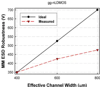
Though HV transistors are designed to sustain voltages ranging from several tens up to more than thousands of volts, their ESD protection levels do not scale with rated blocking voltages. On the contrary, due to their complicated device structures, ESD protection levels are usually poor and hard to engineer. In [7], a strong non-uniform turn-on effect in a HV ESD protection NMOS was observed, i.e. the ESD protection level does not linearly scale with the device dimension. Accordingly, even a large ESD protection device is utilized as the on-chip ESD protection element, a poor ESD protection level can still result. Fig. 1.5 shows the measured MM ESD protection levels of gate-grounded n-channel lateral DMOS (gg-nLDMOS) with different effective channel widths. Strong non-uniform turn-on effect is confirmed comparing the ideal and measured MM ESD robustness.
external inductive loads. Traditionally, the power-rail ESD clamp circuit in Fig. 1.2 is able to help discharge ESD current and is critical to high ESD protection levels. In an open drain or a fail-safe structure, there is no (parasitic) forward diode from input/output (I/O) pad to the VCC
HV power supply line. The power-rail ESD clamp circuit hence does not help discharge ESD current, PS-mode ESD stresses for example (see Fig. 1.6); the ESD protection design at an I/O pad has to take all the ESD current. The open drain structure puts a big challenge to ESD design engineers, and ESD design solutions to the open drain structure are hence valuable to IC industries.
Fig. 1.5. Measured MM ESD protection levels of nLDMOS with different effective channel widths.
Fig. 1.6. ESD current discharging path in an open drain structure. Without a forward diode from the
pad to the HV VCC power supply line, power-rail ESD clamp circuit does not help discharge ESD
Besides the general expectation of a robust electronic system (superior IC reliability), cost is another practical consideration for IC design companies. Cost reduction without downgrading the reliability specification is common to IC industries. Since silicide blocking is dedicated for the purpose of ESD protection, fully-silicided design is straightforward to the cost reduction of silicon chips. To have a fully-silicided design with high ESD robustness, novel design techniques have been being requested by the IC industries and the design challenge is stringent.
1.3. Dissertation Organization
With the above-mentioned ESD design challenges, IC industries are eager to have robust ESD protection solutions so as to enhance product yields and stability. This dissertation accordingly focuses on the improvement techniques to HV MOSFETs’ ESD protection levels. Several new design concepts and practical ESD design solutions that have been realized in commercial IC products are proposed in this dissertation. This dissertation consists of 8 chapters. With the HV N-Well that encloses the nLDMOS, the substrate-triggered technique which is well-known in low-voltage logic technologies is not applicable in the traditional layout method of HV transistors. To alleviate the non-uniform triggering among nLDMOS, a new waffle layout method enabling the body current injection is proposed in chapter 2.
In chapter 3, the safe operating area (SOA) which defines the I-V switching boundaries of a HV transistor is reviewed. SOA characterization methods and improvement methods are discussed in this chapter. The SOA discussion is related to the electrical SOA improvement method in chapter 4 that solves the degraded SOA of an nLDMOS when a silicon controlled rectifier (SCR) is integrated for ESD purposes.
In chapters 5 and 6, there are two fully-silicided ESD solutions that have been implemented on commercial IC products. Designs in chapter 5 enhance ESD protection level
through layout method and are universal to IC products with push-pull output drivers. In chapter 6, the design is specially devised for voltage programming pins that have the fail-safe requirement so as to prevent leakage current when programming internal memories. The ESD design also prevents the latchup-like problem when the programming signal has a fast voltage rise time.
A study to the holding voltage of nLDMOS is included in chapter 7. Holding voltage is a key design consideration for developing high latchup-resistant ESD protection elements. A gradually decreased transistor holding voltage is observed and analyzed by using long-pulse transmission line pulsing (TLP) system [2]. This phenomenon has a negative impact to IC latchup and hence leads to new latchup design considerations.
Chapter 8 summarizes the results of this dissertation and its contribution to future reliability researches. To sum up, this dissertation includes not only new and useful academia ESD research results, but also practical ESD design solutions to the IC industries.
Chapter 2
Waffle Layout Structure With Body-Injected
Technology in BCD High-Voltage Processes
2.1. Background
With the thriving applications in silicon ICs, the demands of HV ICs are increasing rapidly [8]. In HV ICs, the power supply voltage (VCC) is often over ten volts or even higher. To
fabricate devices to sustain such a high operating voltage, not only the process complexity is increased but also the difficulty to guarantee the reliability of HV devices. ESD is an important and inevitable event ICs during fabrication, packaging, and assembling processes [9]–[12]. ESD protection in HV technology is challenging and has received a lot of attention recently [13]–[16].
To improve the ESD robustness of HV NMOS, several techniques related to process modifications have been reported [16]–[20]. The method of inserting N+ buried layer (NBL) has been used to enhance the ESD robustness of nLDMOS [16]. However, additional process steps and mask layers are needed. Besides, a heavily doped P-type body implantation has been used to avoid the non-uniform triggering of parasitic NPN bipolar junction transistors (BJTs) when a HV NMOS is drawn with large array, i.e. large device dimensions (W/L) [20]. In this chapter, the influence of highly doped P-type boron implantation (PBI) layer to the ESD robustness of nLDMOS is first investigated. The nLDMOS was designed to discharge ESD current through the parasitic BJT inherent in the nLDMOS. A circuit and layout co-design method is then proposed to improve ESD robustness of the nLDMOS [21], [22]. The proposed method exploits the body current injection to improve turn-on uniformity of nLDMOS devices during ESD stresses. Therefore, it does not require process modifications or additional mask layers. The proposed method was verified in a 0.5-m 16-V and a
0.35-m 24-V bipolar CMOS DMOS (BCD) process.
(a)
(b)
Fig. 2.1. (a) Layout diagram and the (b) device cross-sectional view along A-A’ line of an nLDMOS in a 0.5-m 16-V BCD process with the optional PBI layer.
2.2. Effect of P-type Boron Implantation on ESD Performance of
High-Voltage nLDMOS
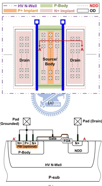
Fig. 2.1(a) shows the traditional (stripe) layout diagram of an nLDMOS in the 0.5-m 16-V BCD process. The nLDMOS in the 0.5-m 16-V BCD process is defined within one
single OD region, so that the gap between N+ drain and the poly gate is the active area. Device cross-sectional view of the 16-V nLDMOS along A-A’ line in Fig. 2.1(a) is shown in Fig. 2.1(b). A PBI layer is optionally implanted underneath the source N+ and P+ regions in the 16-V nLDMOS to investigate its effectiveness on ESD robustness.
(a)
(b)
Fig. 2.2. (a) Layout diagram and the (b) device cross-sectional view along A-A’ line of the nLDMOS in a 0.35-m 24-V BCD process.
For nLDMOS in the 0.35-m 24-V BCD process, drain and source/body regions are defined in different active areas, as shown in Fig. 2.2(a). The gap between N+ drain and poly gate of the nLDMOS device is a field oxide (FOX) region. Device cross-sectional view along
A-A’ line of the 24-V nLDMOS in Fig. 2.2(a) is shown in Fig. 2.2(b). The FOX gap of the 24-V nLDMOS can avoid the field crowding near the drain of nLDMOS, which, in turn, helps the nLDMOS to sustain the high operating voltage of 24 V. In both 16 and 24 V technologies, the nLDMOS devices are surrounded by HV N-Well [23]; P-Body regions in an nLDMOS are fully separated from the common p-type substrate (P-sub). P+ body pick up at every source region is required to bias the P-Body. Channel lengths are defined by the overlapped region of P-Body and the poly gate.
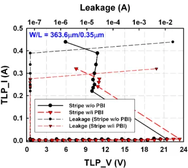
Fig. 2.3. TLP-measured I-V characteristics of gate-grounded 16-V nLDMOS devices with or without the PBI layer.
To analyze characteristics of devices under HBM ESD stresses, TLP system with 100-ns pulse width has been commonly adopted [24], and Fig. 2.3 shows the TLP-measured I-V characteristics of the 16-V nLDMOS with traditional (stripe) layout style. Both 16-V nLDMOS with and without PBI layer in Fig. 2.3 have the same device dimension (W/L) of 363.6 m/0.35 m with each finger width of 45.45 m. From the TLP measurement results, the bipolar trigger voltage (Vt1) of the gate-grounded 16-V nLDMOS without PBI
implantation is 21.4 V. With the heavily doped PBI to reduce the parasitic P-Body resistance, Vt1 of the gate-grounded 16-V nLDMOS is increased to 23.4 V. Because the bipolar beta gain
in the nLDMOS is also suppressed by the PBI layer, holding voltage of the first snapback is slightly increased from 10 to 10.86 V. However, the secondary breakdown current (It2) of the
16-V nLDMOS was found to be degraded from 0.39 to 0.28 A due to the PBI layer.
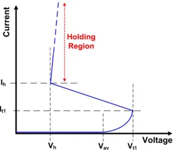
To explain the degradation on ESD robustness of nLDMOS with PBI, the typical I-V characteristic of a gate-grounded NMOS (ggNMOS) during ESD stresses is depicted in Fig. 2.4. When the voltage across the ggNMOS is higher than the reverse drain/body junction breakdown voltage, drain current of the ggNMOS starts to increase due to the avalanche generation. The junction breakdown (VAV) is typically defined as the voltage corresponding
to a 1-A current level of the ggNMOS. Before the avalanche generation current is large enough to forward bias the parasitic body/source junction diode, the ggNMOS acts as a reverse-biased PN junction (HV N-Well/P-Body in Fig. 2.2(b)). Therefore, the voltage keeps increasing without snapback. When the avalanche-generated holes forward bias the body/source junction diode, NPN BJT is turned on to initiate snapback. Due to the turn-on operation of BJT inherent in the ggNMOS, the voltage across the ggNMOS is clamped down to the holding region. The maximum reverse diode current before the snapback of ggNMOS is defined as It1. For devices with large-array design, the effective device width (W) is usually
higher than several thousands of micrometers in order to have high driving capability or low turn-on resistance in specified applications. With a large effective device width, considerable It1 can flow through large-array devices before the BJT triggers. Due to the area consideration,
large array devices are not drawn with ESD design rules and non-uniform triggering among BJT inherent in the large-array device is serious. Consequently, triggering of BJT often induces devastating results to large-array devices [20]. Triggering of BJT has also been reported as the cause of ESD failures in HV power-rail ESD clamp circuits that utilize big field-effect transistors (BigFETs) [25].
Fig. 2.4. The typical I-V characteristic of a gate-grounded NMOS under ESD stresses.
For the 16-V nLDMOS, the heavily doped PBI reduces the effective resistance of P-Body (Rbody); It1 of nLDMOS is increased because turn on of BJT requires (It1 Rbody) Vtdiode,
where Vtdiode is the voltage to forward bias the P-Body/N+ junction diode. Due to the fact that
considerable It1 can flow through large-array nLDMOS where BJT triggering is devastating,
the additional P-type body implantation is beneficial to the ESD robustness of stand-alone large-array nLDMOS. ESD energy is mainly discharged through the reverse diode current (It1)
of the large-array nLDMOS. However, without snapback to clamp down the voltage, large-array nLDMOS is not suitable to protect internal circuits.
For ESD protection nLDMOS devices that are not large-array devices, they usually rely on the turn-on operation of BJT to clamp down ESD voltages to their holding regions and to protect the gate oxide of internal circuits. They are therefore drawn with ESD design rules and the overall effective gate widths are much smaller compared to those of large-array nLDMOS devices. These devices exhibit low It1 because the high current density (It1/W)
makes the P-Body/N+ diode easily forward biased under ESD stresses. As a result, the effect of PBI on increasing It1 is negligible. As shown in Fig. 2.3, both 16-V nLDMOS with and
without PBI implantation exhibit low It1 current. Furthermore, the magnitude of It1 is not
critical for a non-large-array ESD protection nLDMOS. With the bipolar beta gain being suppressed, the measured It2 of nLDMOS was found to be degraded by PBI.
2.3. New Waffle Layout Structure for ESD Improvement
From the measurement results in Fig. 2.3, it is known that the PBI layer degrades ESD robustness of nLDMOS when the nLDMOS device relies on the parasitic BJT to discharge ESD energies. Because the available process modification from foundry is not effective in improving ESD robustness of snapback-based nLDMOS, a layout technique without additional mask or process step is proposed.
In low-voltage (LV) CMOS technologies, one of the most effective methods to increase ESD robustness is the substrate-triggered / substrate-pump technique [26]-[31]. To inject the substrate-triggered current into the base of the parasitic NPN BJT inherent in a LV NMOS, a P+ trigger node was placed at drain and connected to the trigger circuit [27]. However, in HV nLDMOS, the base of its parasitic NPN BJT is surrounded by the HV N-Well. The traditional layout method to inject the substrate-triggered current in LV technologies hence cannot be implemented in HV BCD processes.
To effectively inject the trigger current into the P-Body (the base of NPN BJT), nLDMOS realized in waffle layout style is proposed. Fig. 2.5(a) shows the layout diagram of nLDMOS with the waffle layout style (waffle nLDMOS). In the waffle nLDMOS, the drain of nLDMOS is drawn in a square. Source and body of the waffle nLDMOS are laid out at four sides of the drain square. Such a waffle layout style leads to four squares (Trigger Nodes) at the diagonal corner of a drain square. Both the P-Body regions in the two studied BCD processes are implanted before the formation of gate oxide; therefore the four squares at the diagonal corner of drain are shorted to the body pick up at source/body region. Device cross-sectional views along A-A’ and B-B’ lines of Fig. 2.5(a) are shown in Fig. 2.5(b) and
(a)
(b)
(c)
Fig. 2.5. (a) Layout top view, (b) device cross-sectional view along A-A’, and (c) device cross-sectional view along B-B’, of an nLDMOS with the proposed waffle layout style in the 0.5-m 16-V BCD process. Source/ Body Drain A A’ B’ B Trigger Node
2.5(c), respectively. By using the waffle layout, the body current can be injected from trigger nodes and be collected by the grounded P+ pick up at the source/body. The injected body current acts as the base current to turn on the parasitic NPN BJT. The P+ contacts at source/body in the waffle layout can ensure the grounded body potential during normal circuit operation. Trigger nodes of the waffle nLDMOS are dynamically biased through the circuit co-design method. A trigger circuit is designed to distinguish normal circuit operating and ESD stress conditions [6]. During normal circuit operating conditions, the trigger circuit biases the trigger nodes of the waffle nLDMOS at ground. During ESD stress conditions, the trigger circuit provides the required body injection current to enhance the turn-on uniformity of the waffle nLDMOS.
2.3.1. In the 0.5-m 16-V BCD Process
To verify the ability to turn on the parasitic NPN BJT, a stand-alone waffle nLDMOS with its trigger nodes connected to a bonding pad was injected with different levels of DC body current (IB) through its trigger nodes. Measurement setup is shown in the inset of Fig. 2.6,
where the RBody denotes the equivalent resistance of P-Body from the trigger nodes to the P+
body pick-ups. With the larger injected IB current, the nLDMOS exhibited the higher
collector current IC. This result shows the parasitic NPN BJT can be successfully triggered on
through the body current injection.
To provide the body current during ESD stresses, a trigger circuit composed of a RC distinguisher and a HV inverter was fabricated on-chip. Because the ESD voltage transition has a rise time in the order of nanoseconds but normal circuit power-on transition is in the order of milliseconds, they can be distinguished through a proper design of the RC distinguisher. Corresponding measurement setup to verify the stand-alone trigger circuit is shown in the inset of Fig. 2.7. During the verification measurement, output of the stand-alone trigger circuit was externally short to the trigger nodes of a stand-alone 16-V waffle
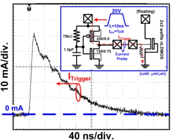
nLDMOS. Fig. 2.7 shows that the trigger circuit can provide a peak trigger current (ITrigger) of
25 mA to the trigger nodes of the stand-alone waffle nLDMOS when a 20-V voltage pulse with 10-ns rise time (tr) and 1-s pulse width (tpw) was applied. After 200 ns, ITrigger fades to 0
mA because of the RC distinguisher.
Fig. 2.6. Turn-on verification of the stand-alone 16-V nLDMOS drawn in waffle style with DC body
current (IB) injected from the trigger nodes.
Fig. 2.7. Turn-on verification of the stand-alone trigger circuit in the 0.5-m 16-V BCD process. The measurement setup is shown in the inset of this figure.
Fig. 2.8. The 100-ns TLP-measured I-V curves of 16-V nLDMOS with stripe, waffle, and body-injected waffle layout style.
The 100-ns TLP-measured I-V curves among the stand-alone stripe, stand-alone waffle, and body-injected waffle nLDMOS devices are shown in Fig. 2.8. The stripe nLDMOS in Fig. 2.8 has the layout style of Fig. 2.1(a). The waffle nLDMOS in Fig. 2.8 has the layout style of Fig. 2.5(a), and the trigger nodes of the waffle nLDMOS are short to source internally. The body-injected waffle nLDMOS in Fig. 2.8 has the layout style as that shown in Fig. 2.5(a), and the trigger nodes in the body-injected waffle nLDMOS were connected internally to the trigger circuit through metal interconnection. The trigger circuit has the same design parameters to the one verified in Fig. 2.7. These three nLDMOS have the same device dimension of 363.6 m/0.35 m in layout. Failure criterion is the same to all devices, 1-A leakage current under 16-V drain bias voltage. Measured results show that the stripe and the waffle nLDMOS have roughly the same secondary breakdown current (It2) of 0.39 and 0.41 A,
respectively, if the body current injection was not applied. By applying the body current injection, It2 of the waffle nLDMOS can be significantly increased from 0.41 to 0.95 A. From
the 100-ns TLP measurement, a more than 2X increase on It2 has been achieved through the
waffle layout style and the body current injection. Measured HBM ESD robustness for stand-alone stripe, stand-alone waffle, and body-injected waffle nLDMOS devices are 0.75, 0.75, and 1.25 kV, respectively.
Fig. 2.9. Scanning electron microscope (SEM) image of the body-injected waffle nLDMOS after 100-ns TLP measurement.
Scanning electron microscope (SEM) image of the body-injected waffle nLDMOS after 100-ns TLP measurement is shown in Fig. 2.9. The failure location of the body-injected waffle nLDMOS was found on the drain of nLDMOS. This result shows that the ESD current is mainly discharged by the nLDMOS instead of the trigger circuit, and confirms the improvement on ESD robustness from the waffle layout and the body current injection.
2.3.2. In the 0.35-m 24-V BCD Process
In the 0.5-m 16-V BCD process, substantial improvement on the ESD robustness of nLDMOS has been achieved by using the waffle layout style along with the trigger circuit to provide body current injection. To study the width scaling to the ESD protection level of
nLDMOS, the circuit and layout co-design technique was fulfilled in a 0.35-m 24-V BCD process.
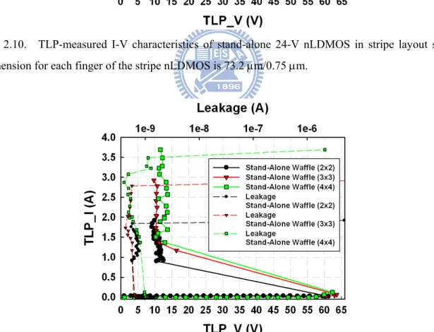
Fig. 2.10. TLP-measured I-V characteristics of stand-alone 24-V nLDMOS in stripe layout style. Dimension for each finger of the stripe nLDMOS is 73.2 m/0.75 m.
Fig. 2.11. TLP-measured I-V characteristics of stand-alone 24-V nLDMOS in waffle layout style. Dimension for each drain square of the waffle nLDMOS is 73.2 m/0.75 m.
(a)
(b)
Fig. 2.12. (a) SEM image of the stand-alone 24-V waffle nLDMOS with 22 drain squares after 100-ns TLP measurement and (b) the enlarged image of ESD the failure locations.
TLP-measured I-V characteristics of stand-alone stripe nLDMOS and stand-alone waffle nLDMOS in the 0.35-m 24-V BCD process are shown in Fig. 2.10 and 2.11, respectively. The measured It2 for stand-alone stripe nLDMOS with 4, 6, 8, and 12 fingers are 1.94, 2.81,
3.15, and 3.16 A, respectively. Each finger of the 24-V stripe nLDMOS is 73.2 m/0.75 m. For stand-alone waffle nLDMOS with 22, 33, and 44 drain squares, the measured It2 are
73.2 m/0.75 m. From the TLP measurement results, non-linear scaling of ESD robustness to the device width was observed on both stand-alone waffle and stand-alone stripe nLDMOS. SEM image of the stand-alone 22 waffle nLDMOS after TLP measurement is shown in Fig. 2.12(a). ESD failures were found only on two drain squares of the 22 stand-alone waffle nLDMOS. Furthermore, the enlarged image of the ESD failure locations in Fig. 2.12(a) is shown in Fig. 2.12(b). Surface current filamentation are observed in Fig. 2.12(b), which implies a superficial current discharging of the stand-alone nLDMOS devices during ESD stresses.
In the 0.35-m 24-V BCD process, ESD detection circuit was also composed of a RC distinguisher and a HV inverter. A stand-alone trigger circuit was fabricated on-chip to verify the driving capability of the trigger circuit, as shown in Fig. 2.13. Corresponding measurement setup and device dimensions of the HV inverter are shown in the inset of Fig. 2.13. Output of the stand-alone trigger circuit was externally short to trigger nodes of a stand-alone waffle nLDMOS. A voltage pulse with 10-ns tr and 1-s tpw was given into the
stand-alone trigger circuit. Measurement result showed a peak ITrigger of 50 mA into the
trigger nodes of the waffle nLDMOS.
Fig. 2.13. Turn-on verification of the stand-alone trigger circuit in the 0.35-m 24-V BCD process. The measurement setup is shown in the inset of this figure.
Fig. 2.14. TLP-measured I-V characteristics of body-injected 24-V nLDMOS with waffle layout style.
Fig. 2.15. Layout diagram of the 24-V stripe nLDMOS with additional P+ trigger bars at upper and bottom of the device for body current injection.
With the body current injection, TLP-measured I-V characteristics for body-injected waffle nLDMOS are shown in Fig. 2.14. TLP-measured It2 for body-injected waffle nLDMOS with
body-injected waffle nLDMOS, the body current injection method was managed to be implemented on the nLDMOS with stripe layout style. As the layout diagram shown in Fig. 2.15, two P+ trigger bars were drawn at two sides of the 24-V nLDMOS with the stripe layout style. Output of trigger circuit was connected internally to these two P+ trigger bars, and these two P+ trigger bars were electrically short to ground through P+ source and the P-Body.
Fig. 2.16. TLP-measured I-V characteristics of body-injected 24-V nLDMOS in stripe layout style.
For body-injected stripe nLDMOS, the studied device has 12 fingers with each finger width of 73.2 m/0.75 m. TLP-measured I-V characteristic for the body-injected stripe nLDMOS is shown in Fig. 2.16. Compare to the stand-alone stripe nLDMOS with 12 fingers, the measured It2 is increased from 3.16 to 4.2 A by using the body current injection.
To compare the ESD performances between different types of nLDMOS, TLP-measured It2
values are normalized to corresponding effective device widths (W) as shown in Fig. 2.17. For stand-alone nLDMOS devices, a slightly higher normalized It2 is found on the stripe
It2 for stand-alone stripe nLDMOS is found to degrade more rapidly than that for stand-alone
waffle nLDMOS. For stripe nLDMOS devices, fingers were drawn in parallel. For waffle nLDMOS devices, drain squares were expanded both horizontally and vertically. As a result, horizontal layout width of stripe nLDMOS is larger than that of waffle nLDMOS. For example, the layout width for the stripe nLDMOS with 12 fingers is 180.2 m; the layout width for the waffle nLDMOS with 4x4 drain squares is 136.5 m. Because bonding pads were in the middle of the DUTs, stripe nLDMOS has a higher mismatch of parasitic metal resistance from the bonding pad to each finger of the nLDMOS. Accordingly, the stand-alone stripe structure shown in Fig. 2.17 shows a severer degradation rate on the normalized It2
values as compared to the stand-alone waffle structure [20].
Fig. 2.17. Normalized It2 current among different types and fingers of 24-V nLDMOS.
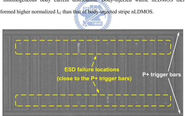
With the body current injection, stripe nLDMOS with P+ trigger bars was found to have normalized It2 lie in between stand-alone nLDMOS devices and body-injected waffle
nLDMOS. SEM image of the body-injected stripe nLDMOS with P+ trigger bars after TLP measurement is shown in Fig. 2.18. From the SEM image, contact spiking was observed in
every finger of the body-injected stripe nLDMOS. However, contact spiking was found only on drain regions near the two P+ trigger bars. No ESD failure was observed in the center portion of the stripe nLDMOS with body current injection. Because the body current was injected from the two P+ trigger bars which was grounded by the P+ body contacts at source side, parasitic BJTs closer to the P+ trigger bars have smaller parasitic P-Body resistance from the P+ trigger bars to the grounded P+ body contacts. As a result, parasitic BJTs closer to the P+ trigger bars receive higher body injection current during ESD stresses. This inhomogeneous body current distribution leads to the result that ESD failures were found to localize on the drain contacts close to the two P+ trigger bars. For nLDMOS devices in waffle layout style, because the side width of each drain square is 18.3 m (much shorter than the 73.2-m finger width of the body-injected stripe nLDMOS), they were less impacted by the inhomogeneous body current distribution. Body-injected waffle nLDMOS thereby performed higher normalized It2 than that of body-injected stripe nLDMOS.
Fig. 2.18. SEM image of the body-injected 24-V nLDMOS with stripe layout style after 100-ns TLP measurement.
From the normalized It2 among different types of nLDMOS devices shown in Fig. 2.17,
style and the body current injection. Body-injected waffle nLDMOS therefore exhibits the highest normalized It2 among different types of nLDMOS shown in Fig. 2.17. Optical beam
induced resistance change (OBIRCH) and SEM images of the body-injected waffle nLDMOS with 44 drain squares after TLP measurement are shown in Fig. 2.19. OBIRCH analysis shows uniform ESD failure locations on the waffle nLDMOS instead of the trigger circuit, which implies that ESD current is properly discharged through the ESD protection nLDMOS. With ESD failures spreading on every drain square of the 44 waffle nLDMOS, SEM image further confirms that uniform triggering of nLDMOS is successfully achieved by using the body current injection. From the TLP measurement results and failure analyses, the effectiveness of body current injection on improving ESD robustness of HV nLDMOS has been verified. ESD robustness of nLDMOS devices studied in this chapter is summarized in Table 2.1.
Fig. 2.19. OBIRCH and SEM images of the body-injected 24-V nLDMOS with waffle layout style after 100-ns TLP measurement.
TABLE 2.1
ESDROBUSTNESS OF NLDMOSDEVICES
2.4. Summary
nLDMOS transistors in HV technologies are known to have poor ESD robustness. Additional P-type boron implantation was found to degrade ESD robustness of snapback-based nLDMOS. Through the collaboration of the proposed waffle layout style and the ESD trigger circuit, the body-injected technique was fulfilled in a 0.5-m 16-V and a 0.35-m 24-V BCD process. The 100-ns TLP measurement results showed substantially improved It2 on waffle nLDMOS. Failure analyses further revealed improvement on the
turn-on uniformity of nLDMOS by the body current injection. From these experimental results, the body-injected technique is effective in increasing the ESD robustness of nLDMOS.
Chapter 3
Overview to The SOA Characterization and
Improvement Techniques in Power MOSFETs
3.1. Background
High voltage and high current operations are common environments for power semiconductor devices. To sustain the high VCC operating voltage, sufficient breakdown
voltage (BVDSS) is a must for power semiconductors. To minimize the power consumption
over a switching transistor, device turn-on resistance per unit area, i.e. the specific on-resistance RSP, is another important factor for the development of power devices. Safe
operating area (SOA), as the third factor to meet the HV and high current requirements, defines the voltage-current boundary in which a power transistor can safely switch. The three factors, BVDSS, RSP, and SOA, are therefore known as the design triangle of power
semiconductor devices as shown in Fig. 3.1 [32].
Fig. 3.1. The design triangle of power semiconductor devices (redrawn after [32]).
3.2. Physical Limitation of SOA
The physical limitation of SOA in a power MOSFET lies in the triggering of intrinsic BJTs [33]. The equivalent circuit model of a HV NMOS is shown in Fig. 3.2. RD, RS, and RB are
current that can forward bias the bipolar base-emitter junction through RB and trigger on the
intrinsic NPN BJT. Major sources of the current Ih include avalanche-generated holes (IAV)
and thermal generation (ITG) due to device self-heating, which can be expressed as
. (3.1)
Fig. 3.2. The equivalent circuit model of a HV NMOS. Parasitic BJT and resistors are included.
Fig. 3.3. The test setup of eSOA measurement with 100-ns TLP.
From equation (3.1), IAV is a result of impact ionization, so that it is a function of both the
drain-source current IDS and avalanche multiplication factor M [33]. To minimize the effect of
stressed by pulses with a short pulse width. Such an electrical SOA (eSOA) boundary is important when thermal effect is not strongly involved during operation; small devices that benefit from good lateral thermal spreading, for example [32]. A 50- TLP system that delivers square pulses with an 100-ns pulse width is usually adopted for the measurement of eSOA [24], [32]. The setup of eSOA measurement is shown in Fig. 3.3, and measured eSOA boundaries of two 24-V nLDMOS are shown in Fig. 3.4. Because snapback (triggering of the intrinsic BJT) usually causes irreversible damage to a power MOSFET or induces circuit malfunctions, the eSOA boundary is defined by sweeping different gate biases and connecting the I-V points right before the device snapback. A higher gate bias causes a reduction in VDS rating because a higher IDS accelerates the number of electron-hole pairs
generated from impact ionization (higher IAV).
Fig. 3.4. Measured eSOA boundaries of two nLDMOS transistors.
When a power MOSFET operates with strong device self-heating, ITG in equation (3.1) can
become the dominating factor to cause device failure. The intrinsic doping concentration (ni)
in a semiconductor device is a strong function of temperature [34]