國 立 交 通 大 學
電子工程學系電子研究所
博 士 論 文
低電壓互補式金氧半製程下的類比電路
設計與可靠度
DESIGN AND RELIABILITY OF ANALOG
CIRCUITS IN LOW-VOLTAGE CMOS
PROCESSES
研 究 生 :陳 榮 昇 (Jung-Sheng Chen)
指導教授 :柯 明 道 (Ming-Dou Ker)
低電壓互補式金氧半製程下的類比電路
設計與可靠度
DESIGN AND RELIABILITY OF ANALOG
CIRCUITS IN LOW-VOLTAGE CMOS
PROCESSES
研 究 生:陳榮昇
Student: Jung-Sheng Chen
指導教授:柯明道
Advisor: Ming-Dou Ker
國 立 交 通 大 學
電子工程學系電子研究所
博 士 論 文
A Dissertation
Submitted to Department of Electronics Engineering
and Institute of Electronics
College of Electrical and Computer Engineering
National Chiao Tung University
in Partial Fulfillment of the Requirements
for the Degree of Doctor of Philosophy
in
Electronic Engineering
September 2007
Hsinchu, Taiwan, Republic of China
i
-低電壓互補式金氧半製程下的類比電路
設計與可靠度
研究生
: 陳榮昇
指導教授: 柯明道 博士
國立交通大學電子工程學系電子研究所
摘要
隨著電子科技的快速發展,電子產品不斷地要求輕、薄、短、小,使
得積體電路(Integrated Circuit)可靠度(Reliability)的重要性與日俱增,許多應
用更需透過奈米級先進製程來實現才能帶來性能上的突破。半導體製程的
微縮化造成電晶體(Transistor)元件尺寸越來越小、閘極氧化層(Gate Oxide)
也越來越薄、和操作電壓也越來越低,所帶來一些元件非理想特性也對類
比電路產生了重大的影響,大大提高了類比積體電路設計難度,其中在低
電壓的操作設計和越來越薄閘極氧化層問題最為嚴重,所以新型低電壓類
比電路設計技術與閘極氧化層的可靠度對類比積體電路之影響是十分重要
的 研 究 主 題 。 本 論 文 提 出 了 一 個 新 型 之 低 操 作 電 壓 能 隙 參 考 電 壓 源
(Bandgap Reference)電路與適用於低操作電壓能隙參考電壓源電路之溫度
曲率補償(Curvature Compensation)技術,並針對閘極氧化層可靠度對類比電
路影響進行研究與分析,另外探討了在奈米互補式金氧半製程中閘極漏電
流(Gate Tunneling Current)對鎖相迴路(PLL)之影響,最後針對低溫多晶矽製
程
(LTPS) 中 提 出 適 用 於 玻 璃 基 板 上 類 比 電 路 設 計 且 具 有 臨 界 電 壓
(Threshold Voltage)補償功能之偏壓電路設計技術。
在第二章中,本論文提出了一個低操作電壓之能隙參考電壓源電路與
一個適於低操作電壓隙參考電壓源電路之溫度曲率補償技術。該新型低操
作電壓能隙參考電壓源電路,最低操作電壓為
0.85 伏特,在此操作電壓之
下,溫度範圍從-10°C 到 120°C 的條件下,能隙參考電壓源電路的輸出電壓
之溫度係數(Temperature Coefficient)為 58.1 ppm/°C,此外,也將提出適於
低操作電壓能隙參考電壓源電路之新型溫度曲率補償技術,經由實際晶片
實現與驗證,此新型溫度曲率補償技術可以在能隙參考電源電路在最低操
作電壓為
0.9 伏特,在溫度範圍從 0°C 到 100°C 的條件下,能隙參考電壓
源電路的輸出電壓之溫度係數可以達到
19.5 ppm/°C。本論文所提出的一個
新型低操作電壓能隙參考電壓源電路與一個適於低操作電壓能隙參考電壓
源電路之新型溫度曲率補償之技術,已經在
0.25 微米互補式金氧半製程中
實現並驗證。
半導體製程的微縮化造成電晶體元件尺寸越來越小、閘極氧化層也越
來越薄,電晶體的閘極氧化層變得更為脆弱更容易遭受破壞,目前已有文
獻針對閘極氧化層可靠度對數位與射頻積體電路影響進行分析與探討,可
是在類比積體電路上仍未有深入的研究與分析。因此,在第三章中,針對
閘極氧化層可靠度對類比電路影響進行研究與分析,針對有無堆疊結構之
主動式負載共源級放大器(Common-Source Amplifier)和雙級式(Two Stage)
與折疊式(Folded Cascade)運算放大器(Operational Amplifier)進行探討,分析
閘極氧化層可靠度對類比電路的影響,並針對閘極氧化層軟式崩潰(Soft
Breakdown)與閘極氧化層硬式崩潰(Hard Breakdown)對類比電路的影響作
了詳細的分析。本論文所探討之測試電路已經在
1 伏 130 奈米互補式金氧
半製程裡實現,並已在
2.5 伏的操作電壓環境下進行分析。
在 低 電 壓 互 補 式 金 氧 半 製 程 中 為 了 使 交 換 式 電 容 電 路
(Switched-
Capacitor Circuit)具有較大的輸入信號範圍與操作速度,因而在交換式電容
iii
-電路中電晶體開關均會利用閘極升壓技術(Gate Bootstrapped Technique)來
設計,可是此設計方式會使得電晶體開關之閘極氧化層跨壓超過正常操作
電壓,長時間操作下會對電晶體開關之閘極氧化層產生破壞。在第四章中,
本論文探討電晶體開關之閘極氧化層可靠度對交換式電容電路的影響。利
用所提出的交換式電容測試電路來進行分析,包括在時域與頻域的波形變
化,並針對閘極氧化層軟式崩潰與閘極氧化層硬式崩潰對交換式電容電路
的影響作了詳細的分析。此測試電路已經在
1.2 伏 130 奈米互補式金氧半
製程中驗證。
鎖相迴路是用來於晶片系統中產生一個精準時脈的電路,為了使鎖相
迴路能夠穩定的操作,在鎖相迴路之迴路濾波電路(Loop Filter)中均需要一
個很大之電容器,通常在晶片上,此電容主要是利用電晶體來實現。當使
用奈米互補式金氧半製程來設計鎖相迴路時,因為越來越薄的閘極氧化層
將會發生嚴重的閘極漏電流問題。因此,在第五章中,本論文探討電晶體
電容之閘極漏電流問題對鎖相迴路的影響,分析鎖相迴路之時基抖動(Jitter)
在時域上受電晶體閘極漏電流的影響。本論文所探討之二階鎖相迴路使用
1 伏 90 奈米互補式金氧半製程之元件模型進行模擬與分析。
顯示系統面板技術的發展,已可在面板基板上加入電子電路,擴張顯
示器產業的應用領域。由於複晶矽薄膜電晶體較傳統用於薄膜電晶體顯示
器面板之非晶矽薄膜電晶體有更大的載子遷移率(Mobility)、較大的驅動電
流、較小的臨界電壓,所以可實現顯示器驅動電路的潛力。然而,目前在
系統面板內建電路設計中,最難克服的一個重點,即為“元件的變動率
(Variation)",相同元件在不同面版上的元件特性可能會有高達~30%的變
動。因此,在第六章中,本論文提出具有臨界電壓補償功能之偏壓電路設
計技術,此技術可以大幅降低元件的變動對偏壓電路的影響,提高類比電
路在玻璃基板上之可行性。本論文所提出之適用於玻璃基板上類比電路設
計且具有臨界電壓補償功能之偏壓電路設計已經在
8 微米低溫複晶矽薄膜
電晶體製程中實現並驗證。
本博士論文提出了一個新型之低操作電壓能隙參考電壓源電路與適用
於低操作電壓能隙參考電壓源電路之溫度曲率補償技術,並針對閘極氧化
層可靠度對類比電路影響進行研究與分析,另外探討了在奈米互補式金氧
半製程中閘極漏電流對鎖相迴路之影響,最後針對低溫多晶矽製程中提出
適用於玻璃基板上類比電路設計且具有臨界電壓補償功能之偏壓電路設計
技術。所提出的電路已在實際晶片上成功驗証,並有相對應的國際會議論
文、國際期刊論文發表。
DESIGN AND RELIABILITY OF ANALOG CIRCUITS IN
LOW-VOLTAGE CMOS PROCESSES
Student: Jung-Sheng Chen Advisor: Dr. Ming-Dou Ker
Department of Electronics Engineering and Institute of Electronics
National Chiao Tung University
ABSTRACT
Due to the growing popularity of electronic technology, the electronic products are continuously asked to reduce its weight, thickness, and volume. So, the reliability of analog integrated circuit is more and more important. Moreover, with the device dimensions of the integrated circuits scaling down, the operation voltage and gate-oxide thickness of device had also been reduced. However, the extra non-ideal effects of devices have great impact on analog integrated circuit to increase design difficulty, such as the lower operation voltage and thin gate oxide. So the new design technique in low-voltage analog integrated circuit and the impact of gate-oxide reliability on performances of analog circuits can be developed. The thinner gate oxide of device will cause the reliability problem in nanoscale analog integrated circuit. In this dissertation, a new sub-1-V CMOS bandgap reference and curvature-compensation technique for CMOS bandgap reference circuit with sub-1-V operation, the impact of gate-oxide reliability on CMOS analog amplifier, the impact of gate tunneling current on performances of phase locked loop, and the new gate bias voltage generating technique with threshold-voltage compensation for on-glass analog circuits in LTPS process are presented. There are seven chapters included in this dissertation.
The new sub-1-V CMOS bandgap reference and curvature-compensation technique for CMOS bandgap reference circuit with sub-1-V operation are presented in Chapter 2. The new proposed CMOS bandgap reference without using low-threshold-voltage device can be
operated with minimum supply voltage of 0.85 V and the temperature coefficient is 58.1 ppm/°C from -10 °C to 120 °C without laser trimming. The new sub-1-V curvature-compensated CMOS bandgap reference, which utilizes the temperature-dependent currents generated from the parasitic NPN and PNP BJT devices in CMOS process, is presented. The new proposed curvature-compensation technique for CMOS bandgap reference circuit with sub-1-V operation has with has been temperature coefficient of 19.5 ppm/°C from 0 °C to 100 °C under minimum supply voltage of 0.9 V without laser trimming.
In general, the VLSI productions have lifetime of 10 years, but the thin gate-oxide thickness of the MOS transistor has many problems, such as gate-oxide breakdown, tunneling current, and hot carrier effect that will degrade the lifetime of the MOS transistor. Therefore, to improve the gate-oxide reliability of MOS transistor and to investigate the effect of gate-oxide breakdown on CMOS circuit performances will become more important in the nanometer CMOS technology. In Chapter 3, the influences of gate-oxide reliability on CMOS analog amplifier are investigated with CMOS common-source amplifiers with diode-connected active load, two-stage and folded-cascade operational amplifiers in a 130-nm low-voltage CMOS process. The test conditions of this work include the dc stress, ac stress with dc offset, and large-signal transition stress under different frequencies and signals. After overstresses, the small-signal parameters, such as small-signal gain, unity-gain frequency, phase margin, and output dc voltage levels, are measured. The impact of soft and hard gate-oxide breakdowns on CMOS analog amplifiers has been analyzed and discussed. The hard breakdown has more serious impact to the CMOS analog amplifiers.
The MOS switch with bootstrapped technique is widely used in low-voltage switched-capacitor circuit. The switched-capacitor circuit with the bootstrapped technique could be a dangerous design approach in the nano-scale CMOS process due to the gate-oxide transient overstress. In Chapter 4, the impact of gate-oxide transient overstress on MOS switch in switched-capacitor circuit is investigated with the sample-and-hold amplifier in a 130-nm CMOS process. After overstress on the MOS switch of SHA with open-loop configuration, the circuit performances in time domain and frequency domain are measured to verify the impact of gate-oxide reliability on circuit performances. The oxide breakdown on switch device will degrade the performance of bootstrapped switch technique.
In nanoscale CMOS technology, the thin gate oxide causes the large gate tunneling leakage. In Chapter 5, the influence of MOS capacitor, as loop filter, with gate tunneling leakage on the circuit performances of phase locked loop (PLL) in nanoscale CMOS
technology has been investigated and analyzed. The basic PLL with second-order loop filter is used to simulate the impact of gate tunneling leakage on performance degradation of PLL in a standard 90-nm CMOS process. The MOS capacitors with different oxide thicknesses are used to investigate this impact to PLL. The locked time, static phase error, and jitter of second-order PLL are degraded by the gate tunneling leakage of MOS capacitor in loop filter. Overview on the prior designs of gate tunneling leakage compensation technique to reduce the gate tunneling leakage on MOS capacitor as loop filter in PLL is provided in this work.
Low-temperature poly-Si LTPS thin-film transistors (TFTs) have attracted a lot of attentions in the applications with the integrated on-panel peripheral circuits for active-matrix liquid crystal display (AMLCD) and active-matrix light emitting diodes (AMOLEDs). Recently, LTPS AMLCDs integrated with driving and control circuits on glass substrate have been realized in some portable systems, such as mobile phone, digital camera, notebook, etc. In the near future, the AMLCD fabricated in LTPS process is promising toward System-on-Panel (SoP) or System-on-Glass (SoG) applications, especially for achieving a compact, low-cost, and low-power display system. However, the poly-Si TFT device suffers from significant variation in its threshold voltage, owing to the nature of poly silicon crystal growth in LTPS process. In Chapter 6, a new proposed gate bias voltage generating technique with threshold-voltage compensation for analog circuits in the low-temperature polycrystalline silicon LTPS thin-film transistors (TFTs) is proposed. The new proposed gate bias voltage generating circuit with threshold-voltage compensation has been successfully verified in a 8-μm LTPS process. The experimental results have shown that the impact of TFT threshold-voltage variation on the biasing circuit can be reduced from 30% to 5% under biasing voltage of 3 V. The new proposed gate bias voltage generating technique with threshold-voltage compensation enables the analog circuits to be integrated and implemented by LTPS process on glass substrate for active matrix LCD (AMLCD) panel.
In summary, several design and reliability of analog circuits in low-voltage CMOS processes are presented in this dissertation. The proposed circuits have been implemented and verified in silicon chips. The proposed CMOS bandgap reference circuits, the impact of gate-oxide reliability on CMOS analog amplifiers, and the proposed gate bias voltage generating technique are very useful for the advanced nanoscale CMOS technology and SoP application, respectively.
ACKNOWLEDGEMENTS
在交通大學電子研究所的生涯中,首先要感謝我的指導教授柯明道教授
在這些年來耐心的指導與鼓勵,使我能順利完成博士學業。不只在專業領
域上的知識,從柯教授認真的研究態度和嚴謹的處事原則,也讓我學習到
克服困難、解決問題的正確態度與方法。此外,感謝
307 實驗室另外四位
師長,吳重雨教授、吳錦川教授、吳介琮教授以及陳巍仁教授給我的指導
與建議。
感謝張志揚教授、林泓均博士、黃弘一教授、姜信欽博士在百忙之中抽
空來擔任我的口試委員,給我指導跟建議,讓整個論文更加完整。
還有謝謝其他
307 實驗室的成員施育全博士、林昆賢博士、林俐如博
士、周儒明博士、李瑞梅博士、陳世倫博士、許勝福博士、王文傑、王文
泰、鄧至剛、徐新智、黃鈞正、張瑋仁、陳勝豪、陳旻珓
、鍾勇輝
、顏承正、
盧台祐
、蕭淵文、謝振宇、蔡夙勇、陳建文、李健銘、陳世宏、陳志豪、
王暢資、王資閔、林群祐、陳穩義、李宇軒、黃俊、莊介堯等學長姐、同
學、學弟們在課業、研究、生活上的幫忙與協助,讓我順利完成我的博士
論文、並學習到做人處事上的態度與方法。此外,感謝
307 實驗室的助理
卓慧貞小姐在實驗室行政事務上的許多協助。
在此還要感謝工業技術研究院系統晶片技術中心、英飛凌上元與中華映
管在實驗晶片下線與量測設備上的幫助,使得我的論文研究成果能在國際
上順利發表,受到肯定。
致上最深的感謝給我親愛的家人們,父親陳進貴先生、母親許淑娥女
士、兄長陳辰雄先生以及其他家人們。有了您們的支持、鼓勵、陪伴和照
顧,才能讓我順利完成學業。還要謝謝女友黃舒瑜小姐,一路上陪伴著我。
最後謝謝所有幫助我、陪著我成長的人。謝謝你們。
陳 榮 昇
誌於竹塹交大
96 年 夏
xi
-CONTENTS
Abstract (Chinese) i Abstract (English) v Acknowledgements (Chinese) ix Contents xi Table Captions xvFigure Captions xvii
Chapter 1. Introduction 1
1.1. CMOS Technology Scaling 1
1.1.1. Device Dielectric Reliability 2
1.1.1.1. Gate-Oxide Breakdown 2
1.1.1.2. Hot Carrier Injection 3
1.1.1.3. Negative Bias Temperature Instability 4
1.1.2. Gate Tunneling Leakage Current 5
1.2. Issues of Circuit Design and Reliability in Low-Voltage CMOS Technology 5
1.3. Organization of This Dissertation 7
Tables 10
Figures 11
Chapter 2. CMOS Bandgap Reference Circuit With Sub-1-V Operation 15
2.1. CMOS Bandgap Reference Circuit for Sub-1-V Operation Without Extra Low-Threshold-Voltage Device 15
2.1.1. Background 15
2.1.2. Traditional Bandgap Reference Circuit 17
2.1.3. Sub-1-V Bandgap Reference Circuit 17
2.1.4. Simulation and Experimental Results 21
2.1.4.1. Simulation Results 21
2.1.4.2. Silicon Verification 21
2.1.5. Summary 22
2.2. Curvature-Compensation Technique for CMOS Bandgap Reference Circuit With Sub-1-VOperation 23
2.2.1. Background 23
2.2.2. Non-Linearity Term of Traditional Bandgap Reference Circuit 24
2.2.3. Sub-1-V Bandgap Reference Circuit With Curvature -Compensated Technique 25
2.2.3.1. Design Concept 25
2.2.3.2. Circuit Implementation 26
2.2.4. Simulation and Experimental Results 29
2.2.4.1. Simulation Results 29 2.2.4.2. Silicon Verification 29 2.2.5. Summary 30 2.3. Conclusion 31 Tables 32 Figures 33
Chapter 3. Impact of Gate-Oxide Reliability on CMOS Analog Amplifiers Circuit in Nanoscale CMOS Technology 43
3.1. Single Amplifier 43
3.1.1. Background 43
3.1.2. Analog Amplifiers 45
3.1.3. Overstress Test 47
3.1.3.1. DC Stress 47
3.1.3.2. AC Stress With DC Offset 49
3.1.3.3. Large-Signal Transition Stress 51
3.1.4. Discussion 53
3.1.5. Effect of Hard and Soft Gate-Oxide Breakdown Performances of Common-Source Amplifiers 54
3.1.5.1. DC Stress 54
3.1.5.2. Large-Signal Transition Stress 56
3.1.6. Summary 58 3.2. Operational Amplifier 58 3.2.1. Background 58 3.2.2. Operational Amplifiers 60 3.2.3. Overstress Test 61 3.2.3.1. DC Stress 62
xiii
-3.2.3.2. AC Stress With DC Offset 67
3.2.3.3. Large-Signal Transition Stress 68
3.2.4. Discussion 69
3.2.5. Effect of Hard and Soft Gate-Oxide Breakdown on Performances of Operational Amplifier 71
3.2.5.1. DC Stress 71
3.2.5.2. Large-Signal Transition Stress 71
3.2.6. Summary 72
3.3. Conclusion 72
Tables 74
Figures 76
Chapter 4. Circuit Performance Degradation of Switched-Capacitor Circuit With Bootstrapped Technique due to Gate-Oxide Overstress 101
4.1. Background 101
4.2. Bootstrapped Technique with Gate-Oxide Reliability 102
4.3. Dependences of Design Parameters on Transient Gate-Oxide Reliability 103
4.3.1. Difference Time Delay between Sampling and Bootstrapped Networks 103
4.3.2. Input/Sampling Frequency Ratio 104
4.4. Switched-Capacitor Circuit With Gate-Oxide Reliability Test Circuit 105
4.5. Experimental Results 107
4.6. Discussion 108
4.7. Summary 110
Figure 111
Chapter 5. Impact of Gate Tunneling Leakage on Performances of Phase Locked Loop Circuit in Nanoscale CMOS Technology 119
5.1. Background 119
5.2. Phase-Locked Loop 120
5.3. MOS Capacitor With Gate Tunneling Leakage Model 121
5.4. Effect of MOS Capacitor With Gate Tunneling Leakage on Performances of PLL Circuit 123
5.6. Overview on the Prior Designs of Loop Filter With Gate Tunneling
Leakage Compensation Technique in PLL 125
5.6.1. Capacitor Structure 125
5.6.2. Opamp Base Compensation Technique 126
5.6.3. Non-Opamp Base Compensation Technique 127
5.6.4. Capaciotr Multiplier 128
5.7. Summary 129
Table 131
Figure 133
Chapter 6. New Gate Bias Voltage Generating Technique With Threshold-Voltage Compensation for On-Glass Analog Circuits in LTPS Process 143
6.1. Background 143
6.2. Impact of Threshold-Voltage Variation on TFT I-V Characteristics 145
6.3. Gate Bias Voltage Generating Technique With Threshold- Voltage Compensation 146 6.3.1. Design Concept 146 6.3.2. Circuit Implementation 147 6.4. Experimental Results 149 6.5. Discussion 150 6.6. Summary 151 6.7. Figure 152
Chapter 7. Conclusions and Future Works 159
7.1. Main Results of This Dissertation 159
7.2. Future Works 162
References 165
VITA 177
TABLE CAPTIONS
Table 1.1. Key Features of the semiconductor scaling trend (High-Performance Logic Technology) [1]. 10 Table 2.1. Comparison among the low voltage bandgap references. 32 Table 2.2. Comparison among the curvature-compensated bandgap voltage references. 32 Table 3.1. Device dimensions of common-source amplifiers with the non-stacked and
stacked diode-connected active load structures. 74 Table 3.2. Comparisons of common-source amplifiers with the non-stacked and stacked
diode-connected active load structures among three overstress conditions. 74 Table 3.3. Device dimensions of operational amplifiers with the two-stage or
folded-cascode structures. 75 Table 3.4. Comparisons of operational amplifiers with the two-stage or folded-cascode
structures among three overstress conditions. 75 Table 5.1. Major gate tunneling leakage mechanisms of MOSFET device in nanoscale CMOS technology [27]. 131 Table 5.2. The summary of gate tunneling leakage per unit area under different
threshold-voltage NMOS and PMOS capacitors in a 90-nm CMOS process. 131 Table 5.3. The design parameters and simulated results of second-order PLL in a 90-nm CMOS process. 131
FIGURE CAPTIONS
Fig. 1.1. Formation of traps in the gate oxide of MOS transistor. 11
Fig. 1.2. Creation of conduction path through traps in the gate oxide of MOS transistor. 11
Fig. 1.3. Increased traps in gate oxide of MOS transistor after Conduction. 12
Fig. 1.4. Cross section of the gate oxide of MOS transistor after hard gate oxide breakdown. 12
Fig. 1.5. Hot carrier injection in CMOS technology. 13
Fig. 1.6. Schematic of the Si/oxide interface of a MOSFET. The dangling Si bonds are present due to the mismatch between the ordered channel and amorphous oxide. These act as interface traps unless they are passivated by hydrogen annealing. NBTI induces the dissociation of the Si–H bonds causing hydrogen to diffuse away from the interface [24]. 13
Fig. 1.7. The cross section of the NMOSFET structure and drain leakage components [28]. 14
Fig. 2.1. The traditional bandgap reference circuit in CMOS technology. 33
Fig. 2.2. The new proposed bandgap reference circuit for sub-1-V operation. 33
Fig. 2.3. Complete schematic of the new proposed bandgap reference. 34
Fig. 2.4. Small signal model of the proposed bandgap reference. 35
Fig. 2.5. Simulated reference voltage of the proposed bandgap reference with different supply voltages. 35
Fig. 2.6. Simulated minimum supply voltage of the proposed bandgap reference. 36
Fig. 2.7. Die photo of the new proposed bandgap reference circuit fabricated in a 0.25-μm CMOS process. 36
Fig. 2.8. Dependence of output reference voltage on the temperature under different VDD voltage levels. 37
Fig. 2.9. Dependence of output reference voltage on the VDD supply voltage under different temperatures. 37
Fig. 2.10. Dependence of PSRR on the frequency under different input sinusoidal amplitudes. 38 Fig. 2.11. The relationship between nonlinear temperature-dependence VBE and linear
voltage reference circuit. The multiplying VPTAT with Kfactor is used to
compensate the VBE. 38 Fig. 2.12. The new proposed sub-1-V curvature-compensated bandgap voltage reference circuit. 39 Fig. 2.13. The cross-sectional view of parasitic vertical NPN BJT in CMOS technology. 39 Fig. 2.14. Complete circuit of the new proposed curvature-compensated bandgap voltage reference for sub-1-V operation. 40 Fig. 2.15. Simulated output reference current (IREF) of the new proposed bandgap voltage reference under different temperatures from 0 to 100 °C with supply voltage of 1 V. 41 Fig. 2.16. Die microphotography of the new proposed curvature-compensated bandgap voltage reference fabricated in a 0.25-μm CMOS process. 41 Fig. 2.17. The measured dependence of output reference voltage on the operating
temperature under different supply voltage levels. 42 Fig. 2.18. The measured dependence of output reference voltage on the supply voltage
under different operating temperatures. 42 Fig. 3.1. Complete circuits of the common-source amplifiers with the (a) non-stacked
and (b) stacked diode-connected active load structures. 76 Fig. 3.2. The measured setup for common-source amplifiers with the non-stacked and stacked diode-connected active load structures under DC stress to investigate the impact of gate-oxide reliability to circuit performances. 77 Fig. 3.3. The dependence of the small-signal gain on the stress time of the
common-source amplifiers with the non-stacked and stacked diode-connected active load structures under the DC stress. 77 Fig. 3.4. The input and output signal waveforms on the different stress times of the
common-source amplifier with the non-stacked diode-connected active load structure under the DC stress. (a) Stress time = 0 min., (b) Stress time = 980 min., and (c) Stress time = 2000 min. 78 Fig. 3.5. The dependence of the unity-gain frequency on the stress time of the
common-source amplifiers with the non-stacked and stacked diode-connected active load structures under the DC stress. 79 Fig. 3.6. The dependence of the output DC voltage level on the stress time of the
common-source amplifiers with the non-stacked and stacked diode-connected active load structures under the DC stress. 79 Fig. 3.7. The measured setup for common-source amplifiers with the non-stacked and stacked diode-connected active load structures under AC stress with DC offset to investigate the impact of gate-oxide reliability to circuit performances. 80 Fig. 3.8. The dependence of the small-signal gain on the stress time of the
common-source amplifiers with the non-stacked and stacked diode-connected active load structures under the stress of the AC small-signal input with DC
offset. 80
Fig. 3.9. The measured setup for common-source amplifiers with the non-stacked and stacked diode-connected active load structures under large-signal transition stress to investigate the impact of gate-oxide reliability to circuit performances. 81 Fig. 3.10. The dependences of the high and low output voltage levels (VH and VL) at the output nodes of the common-source amplifiers with the non-stacked and stacked diode-connected active load structures on the stress time under stress of large-signal transition. 81 Fig. 3.11. The input and output signal waveforms on the different stress times of the
common-source amplifier with the non-stacked and stacked diode-connected active load structures under the large-signal transition stress. (a) Stress time = 0 hour, (b) Stress time = 12 hours, and (c) Stress time = 42 hours. 82 Fig. 3.12. The measured dependence of power supply current IVDD of the
common-source amplifiers with the non-stacked and stacked diode-connected active load structures on stress time under DC stress. 83 Fig. 3.13. The complete circuit of the common-source amplifier with the non-stacked
diode-connected active load structure including the gate-oxide breakdown model. 83 Fig. 3.14. The simulated dependence of power supply current IVDD of the
common-source amplifier with the non-stacked diode-connected active load structure under different resistances of RBD1 and RBD2. 84 Fig. 3.15. The simulated dependence of small-signal gain and output DC voltage level of the common-source amplifier with the non-stacked diode-connected active load structure under different resistances RBD2. 84 Fig. 3.16. The complete circuit of the common-source amplifier with the stacked
diode-connected active load structure including the gate-oxide breakdown model after large-signal transition stress. 85 Fig. 3.17. The simulated dependence of high and low output voltage levels (VH and VL) of the common-source amplifier with the non-stacked diode-connected active load structure under different resistances of RBD1 and RBD2 after large-signal
transition stress. 85 Fig. 3.18. The simulated dependence of high and low output voltage levels (VH and VL) of the common-source amplifier with the stacked diode-connected active load structure under different resistances of RBD3, RBD4, RBD5, and RBD6 after
large-signal transition stress. 86 Fig. 3.19. The complete circuits of the operational amplifiers with the (a) two-stage and (b) folded-cascode circuit structures. 87 Fig. 3.20. The unity-gain buffer configuration for operational amplifiers under DC stress to investigate the impact of gate-oxide reliability to circuit performances. 88 Fig. 3.21. The fresh frequency responses of the operational amplifiers with the (a)
two-stage, and (b) folded-cascode, structures operating in the unity-gain buffer. 89 Fig. 3.22. The dependence of the small-signal gain on the stress time of the operational amplifiers with the two-stage or folded-cascode structures operating in the unity-gain buffer under the DC stress. 90 Fig. 3.23. The dependence of the unity-gain frequency on the stress time of the
operational amplifiers with the two-stage or folded-cascode structures operating in the unity-gain buffer under the DC stress. 90 Fig. 3.24. The dependence of the phase margin on the stress time of the operational
amplifiers with the two-stage or folded-cascode structures operating in the unity-gain buffer under the DC stress. 91 Fig. 3.25. The dependence of the output-voltage swing on the stress time of the
operational amplifiers with the two-stage or folded-cascode structures operating in the unity-gain buffer under the DC stress. 91 Fig. 3.26. The dependence of the offset voltage on the stress time of the operational
amplifiers with the two-stage or folded-cascode structures operating in the unity-gain buffer under the DC stress. 92 Fig. 3.27. The dependence of the rise and fall times on the stress time of the operational amplifiers with the two-stage or folded-cascode structures operating in the
unity-gain buffer under the DC stress. (a) and (b) two-stage operational amplifier. (c) folded-cascode operational amplifier. 93 Fig. 3.28. The dependence of the PSRR on the stress time of the operational amplifiers with the two-stage or folded- cascode structures operating in the unity-gain buffer under the DC stress. 94 Fig. 3.29. The unity-gain buffer configuration for operational amplifiers under the stress of AC small-signal input with DC offset to investigate the impact of gate-oxide reliability to circuit performances. 94 Fig. 3.30. The dependence of the unity-gain frequency on the stress time of the
operational amplifiers with the two-stage structure under the stress of the AC small-signal input with DC offset. 95 Fig. 3.31. The comparator configuration for operational amplifiers under the stress of
large-signal transition to investigate the impact of gate-oxide reliability to circuit performances. 95 Fig. 3.32. The dependences of the high and low voltage levels at the output node on the stress time under stress of large-signal transition. The operational amplifiers with the two-stage or folded-cascode structures are stressed under the comparator configuration. 96 Fig. 3.33. The dependence of the unity-gain frequency on the stress time under the stress of large-signal transition. The operational amplifiers with the two-stage or folded-cascode structures are stressed under the comparator configuration. 96 Fig. 3.34. The measured output voltage swing waveform of operational amplifier with the two-stage structure after DC stress. 97 Fig. 3.35. The complete circuit of the operational amplifier with the two-stage structure including gate-oxide breakdown model under DC stress. 97 Fig. 3.36. The simulated output voltage swing waveform of operational amplifier with the two-stage structure under different breakdown resistances RBD6, RBD7, and
RBD8. 98 Fig. 3.37. The complete circuit of the operational amplifier with the two-stage structure including gate-oxide breakdown model under large-signal transient stress. 98 Fig. 3.38. The simulated high and low output voltage levels of operational amplifier with
the two-stage structure under different breakdown resistances RBD8 and RBD9.
99 Fig. 4.1. (a) Conceptual schematic and (b) detail circuit implementation of bootstrapped
technique for switched-capacitor circuit. 111 Fig. 4.2. Simulated waveforms of gate-oxide transient overstress event in
switched-capacitor circuit with bootstrapped technique. 111 Fig. 4.3. The dependence of the different sampling capacitances on output voltage
waveform in the switched-capacitor circuit with the bootstrapped technique. 112 Fig. 4.4. The dependence of the input/sampling frequency ratio on maximum transient voltage in the switched-capacitor circuit with the bootstrapped technique. 112 Fig. 4.5. The complete circuit of sample-and-hold amplifier with the gate-oxide
reliability test circuit, where the control device MC is used to control the drain
voltage of the switch device MS for reliability test. 113 Fig. 4.6. (a) Chip micrograph and (b) layout view of the sample-and-hold amplifier
with the gate-oxide reliability test circuit realized in a 130-nm CMOS process. 113 Fig. 4.7. The simulated frequency-domain and time-domain waveforms of the
sample-and-hold amplifier with the gate-oxide reliability test circuit under normal operation. 114 Fig. 4.8. The measured frequency-domain and time-domain waveforms of the
sample-and-hold amplifier with the gate-oxide reliability test circuit. (a) Overstress time = 0 hour, and (b) overstress time = 5.2 hours. 115 Fig. 4.9. (a) The sample-and-hold amplifier with the gate-oxide reliability test circuit
including equivalent breakdown resistors RGD and RGS. The simulated
frequency-domain waveforms of the test circuit with equivalent breakdown resistance (b) RGD and (c) RGS of 30 kΩ , respectively. 116 Fig. 4.10. The sample-and-hold amplifier with the gate-oxide reliability test circuit
including equivalent breakdown resistors RGS. The simulated
frequency-domain and time-domain waveforms of the test circuit with equivalent breakdown resistors RGS of 500 kΩ. 117 Fig. 5.1. The basic phase locked loop with second-order low-pass loop filter structure. 133 Fig. 5.2. The second-order loop filter realized with (a) PMOS and (b) NMOS capacitors.
134 Fig. 5.3. (a) Gate tunneling leakage in a thin oxide MOSFET device, and (b) carrier
Fig. 5.4. The simulated dependence of gate tunneling leakage on different threshold-voltage NMOS and PMOS capacitors under different gate voltages in a 90-nm CMOS technology. 136 Fig. 5.5. The simulated control voltage waveforms to find the locked time under MOS capacitors with different oxide thicknesses in second-order PLL. 136 Fig. 5.6. The simulated voltage waveforms to find the static phase error (Δt) under
MOS capacitors with different oxide thicknesses in second-order PLL. 137 Fig. 5.7. The simulated voltage waveforms to find the jitter under MOS capacitors with different oxide thicknesses in second-order PLL. 137 Fig. 5.8. The dependence of different input signal frequencies on jitter and ripple
voltage under different oxide thickness devices in the MOS capacitor of PLL. 138 Fig. 5.9. The schematic of second-order PLL including gate tunneling leakage effect.
138 Fig. 5.10. The schematic of PLL with opamp base gate tunneling leakage compensation circuit by only using thin gate-oxide device [109]. 139 Fig. 5.11. The schematic of PLL with opamp base gate tunneling leakage compensation circuit [111]. 139 Fig. 5.12. The schematic of PLL with non-opamp base gate tunneling leakage
compensation circuit [112]. 140 Fig. 5.13. The loop filter with voltage-mode capacitor multiplier [117]. 140 Fig. 5.14. The schematic of current-mode PLL with current-mode capacitor multiplier
technique [118], [119]. 141 Fig. 6.1. The simulated waveforms of N-TFT drain current ID with 50 %
threshold-voltage variation of Gaussian distribution under different gate voltages VG in a 8-μm LTPS process. 152
Fig. 6.2. The concept of the new proposed gate bias voltage generating technique with threshold-voltage compensation. 152 Fig. 6.3. The complete circuit of the proposed gate bias voltage generating circuit with threshold-voltage compensation for analog circuits in LTPS technology. 153 Fig. 6.4. The simulated gate control voltage VGC of the proposed gate bias voltage
generating circuit with threshold-voltage compensation under different biasing voltages VBIAS. 153
Fig. 6.5. The simulated gate control current VGC of the proposed gate bias voltage
generating circuit with threshold-voltage compensation under the different biasing voltages VBIAS with the 50 % threshold voltage variation (Gaussian
distribution) on N-TFT and P-TFT devices. 154 Fig. 6.6. The simulated drain current ID_MD of the proposed gate bias voltage generating
circuit with threshold-voltage compensation under different biasing voltages VBIAS with the 50 % threshold voltage variation (Gaussian distribution) of
N-TFT and P-TFT devices. 154 Fig. 6.7. The chip photo of the proposed gate bias generating technique with
threshold-voltage compensation fabricated in a 8-μm LTPS process. 155 Fig. 6.8. The measured dependence of variation (%) on the gate voltage VG among four
LTPS N-TFT devices in different panel locations. 155 Fig. 6.9. The measured dependence of variation (%) on the biasing voltage VBIAS
among four LTPS test circuits of the new proposed gate bias generating technique with threshold-voltage compensation in different panel locations.
156 Fig. 6.10. The complete circuit of the proposed gate bias voltage generating circuit with modified N-TFT threshold-voltage referenced current source for analog circuits in LTPS technology. 156 Fig. 6.11. The simulated drain current ID_MD of the proposed gate bias voltage generating
circuit with modified N-TFT threshold-voltage referenced current source under different biasing voltages VBIAS with the 50 % threshold voltage
CHAPTER 1
Introduction
In this chapter, the background of this dissertation is discussed. First, the scaling trend of the CMOS technology is introduced. The device dielectric reliability issue about the gate-oxide breakdown, hot-carrier injection, and negative bias temperature instability in the advanced technology are also discussed. Then, the design and reliability issues of the analog circuits realized in low-voltage CMOS processes are discussed. Finally, the rest of this dissertation is organized.
1.1. CMOS Scaling
The goals of CMOS scaling are to increase the speed and density of the transistors in integrated circuits. Table 1.1 summarizes the key features of the semiconductor scaling trend, which are predicted by the Semiconductor Industry Association (SIA) [1]. The increase of speed requires the higher current density of the transistor due to the load capacitance per unit transistor width has historically remained constant. The drain current (ID) of the NMOS
transistor in the saturation region can be expressed as 2 ( ) (1 ) D n ox GS TH DS W I C V V V L μ λ = ⋅ ⋅ ⋅ − ⋅ − ⋅ , (1.1) ox ox ox C t ε = , (1.2)
where μn is the mobility of the NMOS transistor, Cox is the gate capacitance per unit area of the NMOS transistor, W and L are the channel width and channel length of the NMOS transistor, VTH is the threshold voltage of the NMOS transistor, λ is the channel-length modulation parameter, εox is a dielectric constant of gate oxide, and tox is the oxide thickness. As shown in Table 1.1, the reduction in channel length (L) and the gate oxide thickness (tox) of MOS transistor increase the current density, and more functional MOS transistors can be
fabricated on the same silicon area in advanced CMOS technology. In order to decrease the leakage current and second-order effect of MOS transistor, the operation voltage must be scaled. There three major current leakage phenomenons in short channel MOS device: drain-induced barrier lowering (DIBL), punch-through, and gate-induced drain leakage (GIDL) in advanced CMOS technology. Furthermore, the operation voltage and threshold voltage of MOS transistor are decreased simultaneously for keeping the characteristic and reliability of MOS transistor. In order to decrease the leakage current of MOS transistor, the operation voltage must be scaled. These advances in CMOS circuit performance have been enabled by the miniaturization of MOS device in advanced CMOS technology.
Although the CMOS scaling is toward to increase the speed and the density of MOS transistor, the reliability issue becomes more responsible in the future technologies. The gate oxide thickness and the channel length of MOS transistor are become thinner and shorter, respectively, in future technologies. These result in the gate-oxide breakdown (BD) [2]-[5], hot-carrier injection (HCI) [6], [7], and negative bias temperature instability (NBTI) [8]-[11] issues become more important. Besides, the thinner gate-oxide thickness of MOS transistor also causes extra gate tunneling leakage current. It provides motivation for why design and reliability of integrated circuit is an important issue for future.
1.1.1. Device Dielectric Reliability
The dielectric reliability of MOS transistor includes the ate-oxide breakdown (BD) [2]-[5], hot-carrier injection (HCI) [6], [7], and negative bias temperature instability (NBTI) [8]-[11] issues in advanced CMOS technology. The predominant failure modes of HCI and NBTI are a shift of threshold voltage, device current, and transconductance of MOS transistor over time. The gate-oxide breakdown of MOS transistor causes the dielectric leakage current increases with time under constant voltage stress.
1.1.1.1. Gate-Oxide Breakdown
The gate oxide thickness (tox) of CMOS transistor can be became thinner in order to scale CMOS technology. Since electric fields in the gate oxide are expected to rise with scaling, the long-term reliability of thin gate oxides becomes an important issue in advance
CMOS processes. Gate-oxide breakdown is defined as the time when a cluster of connected bonds, beginning from a “seed” at one interface of the gate-oxide reaches the opposite interface [12]. The gate-oxide breakdown mechanism of MOS transistor in CMOS technology includes the soft gate oxide breakdown and hard gate oxide breakdown.
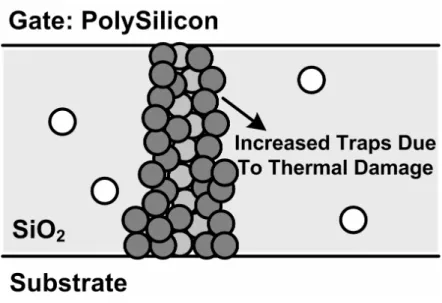
Gate-oxide breakdown begins when traps form in the gate oxide of MOS transistor. At first the traps are non-overlapping and thus do not conduct as shown in Fig. 1.1, but as more and more traps are created in the gate oxide, traps start to overlap creating a conduction path [13]. Once these traps form a conduction path from the gate to the channel, oxide breakdown occurs [13], as shown in Fig. 1.2. This breakdown mode is called soft gate oxide breakdown (SBD). Once there is conduction, new traps are created by thermal damage, which in turn allows for increased conductance as shown in Fig. 1.3 [13]. The cycle of conduction leading to increased heat to increased conduction leads to thermal runaway [14] and finally to a lateral propagation of the breakdown spot [15], as shown in Fig. 1.4. The silicon within the breakdown spot starts to melt, and oxygen is released, and a silicon filament is formed in the breakdown spot [14]. This breakdown mode is called hard gate oxide breakdown (HBD).The lift time of MOS transistor under voltage stress can be expressed as [16]
0 0 1 exp 1 ( ) BD t eff ox G X dt V t τ ⋅ ⎛ ⎞ − ⋅ = ⎜ ⎟ ⎝ ⎠
∫
, (1.3) where τ0 and G are two constants, Xeff is the effective thickness of the gate oxide due to the defeats, and Vox(t) is the time-dependent voltage across the gate oxide, tBD is the time-to-breakdown, and tox is the oxide thickness. The equation 1.3 can be re-written by0 exp ox BD ox G t t V τ ⎛ ⋅ ⎞ = ⋅ ⎜ ⎟ ⎝ ⎠ (1.4) under the DC stress and the defeat-free gate oxide. In equations 1.3 and 1.4, the tox and Vox are two key factors under oxide breakdown. Therefore, the gate-oxide reliability is as very important issue in advanced CMOS technology.
1.1.1.2. Hot-Carrier Injection
thinner and thinner. The short-channel MOS transistor may experience high lateral electric field to cause the hot-carrier injection, if drain-to-source voltage is large. The hot-carrier injection of NMOS transistor is illustrated in Fig. 1.5 [17]. When the channel of NMOS transistor is formed (VG>VTH) and a large drain-to-source voltage (VDS) is applied, 1.
electrons are accelerated by the large lateral electric field. 2. These electrons arrive to the drain depletion region and create electron-hole pairs through impact ionization. 3. If the generated electron has more than approximately 1.5 eV, they can tunnel into the oxide region. The trapped charge in oxide region of MOS transistor will decrease the saturation current IDS,
cause the threshold voltage drift, decrease the linear region transconductance, and degrade the sub-threshold slop. 4. The generated holed will be collected by source and substrate. This will result in that the snapback breakdown or latch-up occurs in MOS transistor to cause the large current into the substrate. Lightly doped drain (LDD) structure can be used in the advanced processes to allow the higher drain-source voltage without the hot-carrier degradation [17]-[20]. However, the LDD structure increases the series drain resistance, which degrades the speed performance.
1.1.1.3. Negative Bias Temperature Instability
Negative bias temperature instability (NBTI) occurs in PMOS transistor stressed with negative gate bias at elevated temperatures. NBTI degradation in MOSFETs is explained by the reaction-diffusion (RD) model mentioned in [21]–[24]. The hydrogen gas diffuses into the gate-oxide and yields passivated Si bonds, as shown in Fig. 1.6 [24]. The hydrogen-annealing technique has provided a viable solution to the interface-trap instabilities for decades; however, recent scaling trends and processing modifications have brought NBTI into attention. According to the standard reaction–diffusion model for NBTI, for a negatively biased PMOS transistor, the holes in the inversion layer react with the Si-H bonds at the Si/SiO2 interface. This leads to the dissociation of the Si-H bonds and results in Si- dangling
bonds at the interface. The generated hydrogen species diffuse away from the interface toward the polysilicon gate. In the absence of holes near the interface, a reverse reaction takes place in which hydrogen species diffuse back to the Si/SiO2 interface and react with Si-bonds
to anneal the generated interface states [21]–[24]. Specifically, negative bias temperature instability causes systematic reduction in transistor parameters, such as drain current, transconductance, threshold voltage, capacitance, when a PMOSFET is biased in inversion (VS=VD=VB=VDD and VG=0).
Advances in technology have raised many new issues related to both circuit performance and reliability. Since electric fields in the gate oxide are expected to rise with scaling, the long-term reliability of thin oxides becomes an important concern in advanced CMOS processes. As described in sections 1.1.1, 1.1.2, and 1.1.3, the CMOS scaling causes many reliability issues in advanced CMOS technology, such as gate-oxide breakdown, hot carrier injection, and negative bias temperature instability.
1.1.2. Gate Tunneling Leakage Current
According to the SIA roadmap [1], CMOS with gate length below 70 nm will need an oxide thickness of less than 1.5 nm, which corresponds to two to three layers of silicon dioxide atoms.With such a thin gate oxide, direct tunneling occurs resulting in an exponential increase of gate leakage current [25]-[31]. The resulting gate leakage current will increase the power dissipation and will deteriorate the device performance and circuit stability for VLSI circuits. Control of off-state drain leakage (Ioff) and on-state gate leakage (IG) is one of the
most important issues for scaling MOSFETs toward the 0.10 μm regime [25]-[31]. For deep submicron technology, as effective gate length decreases, the leakage increases because of the following scaling trends: 1) subthreshold leakage (Isub)increases exponentially due to
threshold voltage reduction [29]; 2) gate edge-direct-tunneling leakage (IEDT) and
gate-induced drain-leakage (IGIDL) increase exponentially due to reduced gate oxide thickness
[30], [31]; 3) bulk band-to-band-tunneling leakage (IB-BTBT) increases exponentially due to
increased lightly doped-drain (LDD) or pocket-doping concentrations [29]. The cross section of the NMOSFET structure and drain leakage components are schematically shown in Fig. 1.7 [28]. The off-state drain leakage (Ioff) and on-state gate leakage (IG) of MOSFET will
increase the power consumption and degrade the performances of integrated circuit in advanced CMOS technology. The high-K gate dielectrics of MOSFET can be used to avoid the gate leakage effect in advanced CMOS technology [32]-[34].
1.2. Issues of Analog Circuit Design and Reliability in
Low-Voltage CMOS Technology
systems in battery-operated products, such as cell phones, PDAs and notebooks. The device dimension of transistor has been scaled toward the nanometer region and the power supply voltage of chips in the nanoscale CMOS technology has been also decreased due to the reliability and power consumption issues [1]. Voltage reductions guarantee the reliability devices to low the electrical fields inside oxide layers of MOSFET. As shown in Table. 1.1, the power supply voltage is decreased and the oxide thickness is thinner when the process is scaled down. Because of noise and offset voltage constraints, the minimum size transistors cannot be used in analog circuit. However, scaling results in better performance in digital circuit. When analog circuit operates in low voltage, the main constraints are the device noise level and the threshold voltage (VTH). The reduction of threshold voltage is dependent on the
device technology. High threshold voltage gives better noise immunity and lower threshold voltage reduces the noise margin to result in poor signal-to-noise ratio (SNR) [35]. In order to get the better performance of analog circuit in low-voltage CMOS technology, a possible solution to get higher DC voltage on-chip is multiplication. However, this technique is noisy and not compatible with sensitive analog circuit. Another problem of this technique is gate-oxide reliability. Many design technique of analog circuit in low-voltage CMOS technology have been proposed, such as MOSFET operated in sub-threshold region [35]-[37], bulk driven transistors [35], [36], [38], [39], self-cascode structures [35], floating gate approach [35], [40]-[44], and level shifter techniques [35], [45]-[47].
In general, the VLSI productions have lifetime of 10 years, but the thin gate-oxide thickness of the MOS transistor has many problems, such as gate-oxide breakdown, tunneling current, and hot carrier effect that will degrade the lifetime of the MOS transistor. Another important problem in low-voltage CMOS technology is the gate-oxide reliability. In modern CMOS very large scale integrated circuits (VLSIs) including digital signal processor and embedded analog circuitry, the digital logic or digital logic circuits are generally implemented using thin-oxide devices. However, analog circuitry needs to be operated at a higher supply voltage than the nominal supply voltage of thin-oxide devices to achieve a wide dynamic range performance or meet the compatibility requirement with standardized protocols or with ICs from previous generations [48]. High-voltage tolerance of analog circuit design technique in nanoscale CMOS technology has been proposed [48]. Therefore, to improve the gate-oxide reliability of MOS transistor and to investigate the effect of gate-oxide breakdown on CMOS circuit performances will become more important in the nanometer CMOS technology. The impact of gate-oxide reliability on CMOS digital and RF
circuit has been investigated [49]-[52]. Reference [49] has reported that the oxide breakdown do not affect the digital circuit operation. Only the power consumption of digital circuit will be increased due to the gate-oxide breakdown. Reference [50] has reported the performances of dynamic digital circuit are degraded by gate-oxide breakdown. In [51], [52], the performances of RF and SRAM circuits are also degraded by gate-oxide breakdown. However, the impact of gate-oxide breakdown on CMOS analog circuits did not have particular report.
Therefore, in this dissertation, several sub-1-V bandgap reference circuits and the impact of gate-oxide reliability on analog circuits in low-voltage CMOS technology are investigated and presented.
1.3. Organization of This Dissertation
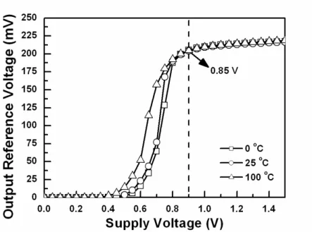
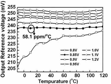
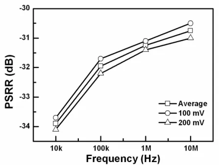
In Chapter 2, a new sub-1-V CMOS bandgap voltage reference without using low-threshold-voltage device is presented in this paper. The new proposed sub-1-V bandgap reference with startup circuit has been successfully verified in a standard 0.25-μm CMOS process, where the occupied silicon area is only 177 μm × 106 μm. The experimental results have shown that, with the minimum supply voltage of 0.85 V, the output reference voltage is 238.2 mV at room temperature, and the temperature coefficient is 58.1 ppm/°C from -10 °C to 120 °C without laser trimming. Under the supply voltage of 0.85 V, the average power supply rejection ratio (PSRR) is -33.2 dB at 10 kHz. The new sub-1-V curvature-compensated CMOS bandgap reference, which utilizes the temperature-dependent currents generated from the parasitic NPN and PNP BJT devices in CMOS process, is presented. The new proposed sub-1-V curvature-compensated CMOS bandgap reference has been successfully verified in a standard 0.25-μm CMOS process. The experimental results have confirmed that, with the minimum supply voltage of 0.9 V, the output reference voltage at 536 mV has a temperature coefficient of 19.5 ppm/°C from 0 °C to 100 °C. With 0.9-V supply voltage, the measured power noise rejection ratio is -25.5 dB at 10 kHz.
In Chapter 3, the influence of gate-oxide reliability on common-source amplifiers with diode-connected active load is investigated with the non-stacked and stacked structures under analog application in a 130-nm low-voltage CMOS process. The test conditions of this work
include the DC stress, AC stress with DC offset, and large-signal transition stress under different frequencies and signals. After overstresses, the small-signal parameters, such as small-signal gain, unity-gain frequency, phase margin, and output DC voltage levels, are measured to verify the impact of gate-oxide reliability on circuit performances of the common-source amplifiers with diode-connected active load. The small-signal parameters of the common-source amplifier with the non-stacked diode-connected active load structure are stronger degraded than that with non-stacked diode-connected active load structure due to gate-oxide breakdown under analog and digital applications. The common-source amplifiers with diode-connected active load are not functional operation under digital application due to gate-oxide breakdown. The impact of soft and hard gate-oxide breakdowns on common-source amplifiers with non-stacked and stacked diode-connected active load structures has been analyzed and discussed. The hard breakdown has more serious impact to the common-source amplifiers with diode-connected active load. The effect of the MOSFET gate-oxide reliability on operational amplifier is investigated with the two-stage and folded-cascode structures in a 130-nm low-voltage CMOS process. The test operation conditions include unity-gain buffer (close-loop) and comparator (open-loop) configurations under the DC stress, AC stress with DC offset, and large-signal transition stress. After overstress, the small-signal parameters, such as small-signal gain, unity-gain frequency, and phase margin, are measured to verify the impact of gate-oxide reliability on circuit performances of the operational amplifier. The gate-oxide reliability in the operational amplifier can be improved by the stacked configuration under small-signal input and output application. A simple equivalent device model of gate-oxide reliability for CMOS devices in analog circuitsis investigated and simulated.
In Chapter 4, the MOS switch with bootstrapped technique is widely used in low-voltage switched-capacitor circuit. The switched-capacitor circuit with the bootstrapped technique could be a dangerous design approach in the nano-scale CMOS process due to the gate-oxide transient overstress. The impact of gate-oxide transient overstress on MOS switch in switched-capacitor circuit is investigated with the sample-and-hold amplifier in a 130-nm CMOS process. After overstress on the MOS switch of SHA with open-loop configuration, the circuit performances in time domain and frequency domain are measured to verify the impact of gate-oxide reliability on circuit performances. The oxide breakdown on switch device will degrade the performance of bootstrapped switch technique.
In Chapter 5, the thin gate oxide causes the large gate tunneling leakage innanoscale CMOS technology. In this work, the influence of MOS capacitor, as loop filter, with gate tunneling leakage on the circuit performances of phase locked loop (PLL) in nanoscale CMOS technology has been investigated and analyzed. The basic PLL with second-order loop filter is used to simulate the impact of gate tunneling leakage on performance degradation of PLL in a standard 90-nm CMOS process. The MOS capacitors with different oxide thicknesses are used to investigate this impact to PLL. The locked time, static phase error, and jitter of second-order PLL are degraded by the gate tunneling leakage of MOS capacitor in loop filter. Overview on the prior designs of gate tunneling leakage compensation technique to reduce the gate tunneling leakage on MOS capacitor as loop filter in PLL is provided in this work.
Chapter 6 presents a new proposed gate bias voltage generating technique with threshold-voltage compensation for analog circuits in the low-temperature polycrystalline silicon LTPS thin-film transistors (TFTs). The new proposed gate bias voltage generating circuit with threshold-voltage compensation has been successfully verified in a 8-μm LTPS process. The experimental results have shown that the impact of TFT threshold-voltage variation on the biasing circuit can be reduced from 30% to 5% under biasing voltage of 3 V. The new proposed gate bias voltage generating technique with threshold-voltage compensation enables the analog circuits to be integrated and implemented by LTPS process on glass substrate for active matrix LCD (AMLCD) panel.
Chapter 7 summarizes the main results of this dissertation. Then, some suggestions for the future works are also addressed in this chapter.
Table 1.1
Key Features of the Semiconductor Scaling Trend (High-Performance Logic Technology) [1]
Fig. 1.1. Formation of traps in the gate oxide of MOS transistor.
Fig. 1.3. Increased traps in gate oxide of MOS transistor after Conduction.
Fig. 1.5. Hot carrier injection in CMOS technology [17].
Fig. 1.6. Schematic of the Si/oxide interface of a MOSFET. The dangling Si bonds are present due to the mismatch between the ordered channel and amorphous oxide. These act as interface traps unless they are passivated by hydrogen annealing. NBTI induces the dissociation of the Si–H bonds causing hydrogen to diffuse away from the interface [24].
CHAPTER 2
CMOS Bandgap Reference Circuit With
Sub-1-V Operation
In this chapter,two sub-1-V CMOS bandgap voltage references without using low-threshold-voltage device are presented. First, the new proposed sub-1-V bandgap reference with startup circuit has been successfully verified in a standard 0.25-μm CMOS process, where the occupied silicon area is only 177 μm × 106 μm. The experimental results have shown that, with the minimum supply voltage of 0.85 V, the output reference voltage is 238.2 mV at room temperature, and the temperature coefficient is 58.1 ppm/°C from -10 °C to 120 °C without laser trimming. Under the supply voltage of 0.85 V, the average power supply rejection ratio (PSRR) is -33.2 dB at 10 kHz. Second, a new sub-1-V curvature-compensated CMOS bandgap reference, which utilizes the temperature-dependent currents generated from the parasitic NPN and PNP BJT devices in CMOS process, is presented. The new proposed sub-1-V curvature-compensated CMOS bandgap reference has been successfully verified in a standard 0.25-μm CMOS process. The experimental results have confirmed that, with the minimum supply voltage of 0.9 V, the output reference voltage at 536 mV has a temperature coefficient of 19.5 ppm/°C from 0 °C to 100 °C. With 0.9-V supply voltage, the measured power noise rejection ratio is -25.5 dB at 10 kHz.
2.1. CMOS Bandgap Reference Circuit for Sub-1-V
Operation Without Extra Low-Threshold-Voltage
Device
Low voltage and low power are two important design criteria in both analog and digital systems. It has been expected that the whole electronic system will be operated down to a single 1-V supply in near future. The bandgap reference (BGR) generators which can be operated under 1-V supply have been widely used in DRAM, flash memories, and analog-to-digital converter (ADC). So far, many techniques have been proposed to develop voltage or current references, which can be almost independent to temperature and power-supply voltage. The bandgap reference is the major design to provide a precision voltage reference with low sensitivity to the temperature and the supply voltage.
When CMOS technologies enter the nano-scale eras, the demand for battery-operated portable equipments will increase. The supply voltage has been scaled down from 1.8 V (in 0.18-μm technology) to 1.2 V (in 0.13-μm technology), and will drop to only 0.9 V in the next generation technology [53]. In CMOS technology, the parasitic vertical bipolar junction transistor (BJT) had been commonly used to implement P-N junction of the bandgap reference. But, the traditional CMOS bandgap reference circuits did not work in sub-1-V supply voltage. The reason, that the minimum supply voltage can not be lower than 1 V, is constrained by two factors. One is the bandgap voltage of around 1.25 V in silicon [54]-[63], which exceeds 1 V supply. The other factor is that the low-voltage design of the proportional to absolute temperature current generation loop is limited by the input common-mode voltage of the amplifier [54], [57]. These two limitations can be solved by using the resistive subdivision methods [55], [59], low-threshold voltage (or native) device [58]-[60], BiCMOS process [57], or DTMOST device [61]. However, those approaches often require specialized processes and characterization, which increase fabrication cost and process steps.
In this work, a new bandgap reference is proposed, which can be successfully operated with sub-1-V supply in a standard 0.25-μm CMOS process without special process technology [64]. Without laser trimming, the new proposed bandgap voltage reference has been proven in the silicon chip with a stable output voltage VREF of
238.2 mV at room temperature and a temperature coefficient of 58.1 ppm/°C under VDD power supply of 0.85 V.
2.1.2. Traditional Bandgap Reference Circuit
A typical implementation of bandgap reference in CMOS technology is shown in Fig. 2.1. In this circuit, the output is the sum of a base-emitter voltage (VEB) of BJT
and the voltage drop across the upper resistor. The BJTs (Q1 and Q2) are typically
implemented by the diode-connected vertical PNP bipolar junction transistors. The output voltage of the traditional bandgap reference circuit can be written as
2 1 - 2 1 2 ln REF TRAD EB T R A V V V R A ⎛ ⎞ = + ⎜ ⎟ ⎝ ⎠, (2.1) where A1 and A2 is the emitter areas of Q1 and Q2, and VT is the thermal voltage. The
second item in (2.1) is proportional to the absolute temperature (PTAT), which is used to compensate the negative temperature coefficient of VEB. Usually, the VPTAT voltage
comes from the thermal voltage VT with a temperature coefficient about + 0.085
mV/°C, which is quite smaller than that of VEB. After multiplying VPTAT with an
appropriate factor and summing with VEB, the bandgap reference will have a very low
sensitivity to temperature. Hence, if a proper ratio of resistors is kept, an output voltage with very low sensitivity to temperature can be obtained. In general, the VREF
is about 1.25 V in CMOS process, so that the traditional bandgap reference circuit can not be operated in low voltage application, such as 1 V or below.
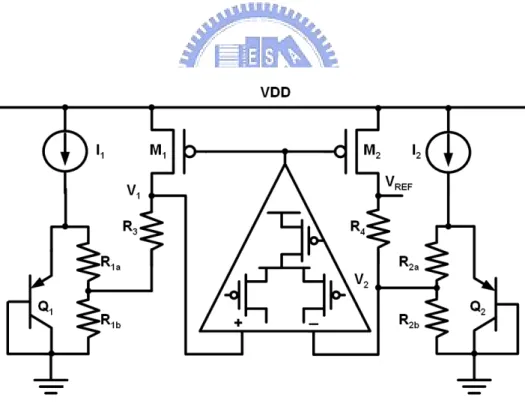
2.1.3. New Proposed Bandgap Reference Circuit
The design concept of the new proposed bandgap reference is that the two voltages (which are proportional to VEB and VT, respectively) are generated from the
same feedback loop. The two-stage operational amplifier with p-channel input is used in this new proposed bandgap reference. The p-channel input has a lower input common-mode voltage than that of the n-channel input to keep the transistors working in the saturation region.
The new proposed bandgap reference is shown in Fig. 2.2, which uses the resistive subdivision R1a, R1b,R2a, and R2b to reduce the input common-mode voltage
![Fig. 1.7. The cross section of the NMOSFET structure and drain leakage components [28]](https://thumb-ap.123doks.com/thumbv2/9libinfo/8144002.166780/40.892.191.703.172.501/fig-cross-section-nmosfet-structure-drain-leakage-components.webp)