國 立 交 通 大 學
電子工程學系 電子研究所
碩 士 論 文
氟化緩衝層應用於接觸孔蝕刻停止層局部形
變矽金氧半場效電晶體鈍化層之特性與研究
Characteristics and Investigation of
FSG buffer Layer on CESL Local strained-Si
HfO
2/SiON Gate Stack MOSFETs
研 究 生:李翊裳
Yi-Shang Li
指導教授:羅正忠 博士
Dr. Jen-Chung Lou
氟化緩衝層應用於接觸孔蝕刻停止層局部形變
矽金氧半場效電晶體鈍化層之特性與研究
Characteristics and Investigation of
FSG buffer Layer on CESL Local strained-Si
HfO
2/SiON Gate Stack MOSFETs
研 究 生:李翊裳 Student:Yi-Shang Li
指導教授:羅正忠 博士 Advisor:Dr. Jen-Chung Lou
國 立 交 通 大 學
電子工程學系 電子研究所碩士班
碩 士 論 文
A Thesis
Submitted to Department of Electronics Engineering & Institute of Electronics College of Electrical and Computer Engineering
National Chiao Tung University In Partial Fulfillment of the Requirements
For the Degree of Master of Science In
Electronics Engineering September 2010
Hsinchu, Taiwan, Republic of China
氟化緩衝層應用於接觸孔蝕刻停止層局部形變
矽金氧半場效電晶體鈍化層之特性與研究
研究生:李翊裳
指導教授: 羅正忠博士
國立交通大學 電子工程學系 電子研究所碩士班 摘 要 隨著互補式金氧半場效電晶體元件尺寸的微縮,卻遭遇到微影製程發展的瓶 頸導致微縮的困難,故近年來發展出了形變矽技術以增進驅動電流。但形變矽技 術也遭遇到了熱載子效應(HCI)以及閘極漏電流上升的問題。 在193奈米濕浸式微影技術發展出來後,元件尺寸得以繼續微縮,但卻又發 現極薄的二氧化矽介電質層將遭遇漏電流過大的物理限制,導致元件可靠度上的 問題。近年來使用高介電質材料取代傳統以二氧化矽當介電質層已廣泛地被研究。 相較於二氧化矽,由於在相同的等效厚度之下高介電質物質有較厚的實際厚度, 因此可以抵擋因量子的穿遂效應而導致的大量漏電。然而以高介電質材料當閘極 介電質層會衍生出其它問題。例如:相對於二氧化矽操作在相同電壓下,高介電 質材料有較高的界面狀態產生及較多的電荷捕捉,這對於元件操作時臨限電壓的 漂移有嚴重的影響。
效能,並提出與現有製程具高度相容性的四氟化碳電漿處理技術,利用此一技術 形成氟化矽玻璃(FSG)作為n型金氧半場效電晶體的第一層鈍化層,並於之後鍍上 氮化矽為第二層鈍化層以達成局部形變矽,在最後sintering修補金屬介面斷鍵 過程中,加熱使氟原子有效擴散至高介電閘極本體和介面通道處,實驗結果顯示 加入FSG後氟原子能修補介面中的缺陷,使驅動電流獲得改善,並且降低次臨界 擺幅和閘極漏電流。 此外也分析可靠度劣化程度,在固定電壓應力(CVS)和熱載子應力(HCS)可靠 度特性上皆有改善的效果,實驗結果顯示在應力破壞下,FSG樣本均有較小的臨 界電壓偏移,表示有較少的本體電子捕捉與界面狀態密度改變,這些元件電性獲 得改善及具有高可靠性的呈現,原因是來自於氟原子擴散入高介電閘極主體以及 閘極層與通道界面間,不僅可減少界面狀態的懸空鍵結和界面狀態陷阱產生,並 進一步有效減少高介電閘極主體電荷捕捉情形。
Characteristics and Investigation of
FSG buffer Layer on CESL Local strained-Si
HfO
2/SiON Gate Stack MOSFETs
Student : Yi-Shang Li Advisor : Dr. Jen-Chung Lou
Department of Electronics Engineering & Institute of Electronics National Chiao Tung University
Abstract
With the complementary MOS transistor device size scaling, the development of lithography process encountered bottlenecks lead to difficulties in scaling , so in recent years developed a strained silicon technology to enhance the drive current. But the strained silicon technology has also suffered the effects of hot carrier injection (HCI) and the increase in gate leakage current problem.
In the 193-nm immersion lithography technology developed, the component size to continue scaling, but it is found in very thin silicon dioxide dielectric layer will suffer too much leakage current physical limitations, leading to device reliability
problems. In recent years the use of high dielectric material to replace traditional silicon dioxide gate dielectric layer as has been studied extensively. Compared to silicon dioxide, because under the same equivalent thickness , high dielectric material has the thicker actual thickness , it can withstand large leakage current caused by quantum tunneling effect. However, high dielectric materials as gate dielectric layer will rise to other problems. For example: relative to silicon dioxide in the same operation voltage, high-dielectric material has a more higher interface states and charge trapping , this has serious implications for the device operation threshold voltage drift.
This article discusses the local strain-si technology for hafnium oxide gate stack MOS transistor performance, and also make the existing process with a high degree of compatibility of the fluorine plasma processing technology, use this technique to form fluoride of silicon glass (FSG) as the n-type MOS transistor of the first layer of passivation layer, and later deposited silicon nitride passivation layer as the second layer to construct the local strain, at the final sintering process, the heat giving energy make fluorine atoms effectively diffuse into bulk and high-k dielectrics interface channel, the results appear that the FSG fluorine atoms in the interface repair damage to improved drive current and lower subthreshold swing and gate leakage current. We also analyzed the degree of reliability degradation, the reliability
characteristics of the constant voltage stress (CVS) and the hot carrier stress (HCS) has been improved, experimental results show that under the stress of destruction, FSG sample have a smaller threshold voltage shift that there is less bulk electron trapping and interface state density changes, and because the fluorine atoms that diffused into high-k gate layer and the interface not only can reduce the interface dangling bond and the interface state trap generation, and further reduce the electrons caputured by high k gate, these decvices have improved electrical properties and high reliability of the present.
誌謝
三年的碩士研究生活,在轉眼間就要面對結束的時刻了,在踏入另一
段未知且具挑戰的旅途前,謹在此表達我想對你們說的話。
首先,當然要先感謝我的指導教授羅正忠博士,從羅教授那學到了許
多研究方法和經驗;其次要感謝謝智仁學長及威良學長在我研究題目
觀念及量測技巧的指導,希望學長們在未來的研究與生涯能夠一帆風
順;再來感謝我的家人,在這三年中在我背後默默地給我支持和力量,
希望你們身體健康;同時謝謝同在實驗室努力的學弟妹們:文新、尚
勳、芳毓,以及劍道社的同伴們,有了你們的陪伴以及幫忙,精神上
能夠得到倚靠,讓我在實驗上能夠解決許多的問題及困難。
在這碩士生涯中,有痛苦到牙齒緊咬的事,也有開心到手舞足蹈的事,
這些我都虛心接受成為記憶的一部分,畢竟這些都是成長自己的機
會。
感謝自己的緣分能遇到你們,也期待以後有緣能再相聚。
Contents
Abstract (Chinese)………...i
Abstract (English) ………...iii
Acknowledgement………..……….vi
Contents………...……...vii
Table Captions……...………...……..….…………ix
Figure Captions………..……..…...x
Chapter 1 Introduction ··· 1
1.1 Background ··· 1
1.2 Motivation ··· 3
1.3 Recent locally strain technology ··· 5
1.4 Enhancing Robustness by Fluorine ··· 8
1.5 Organization of This Thesis ··· 10
Chapter 2 Local strained-Si on HfO
2/SiON nMOSFETs ··· 14
2.1 Mobility degradation by high-k materials ··· 14
2.2 Mobility enhanced by local strained-si ··· 14
2.3 Local strained-si induced Serious hot carrier injection
phenomenon ··· 19
Chapter 3 Experimetal Result and discussion of Local strained-Si
HfO2/SiON nMOSFETs with FSG passivation layer ··· 24
3.1 Experiment ··· 24
3.2 Measurement setup ··· 26
3.3 Result and discussion ··· 27
3.3.1 Electrical characteristics of high-k gate stack
nMOSFETs with different P.L. ··· 27
3.3.2 Reliability characteristics of high-k gate stack
nMOSFETs with different P.L. ··· 29
3.4 Summary ··· 31
Chapter 4 Conclusions and Suggested Future Works ··· 52
4.1 Conclusions ··· 52
4.2 Suggestion for Future Works ··· 53
References ··· 55
Table Captions
Chapter 01
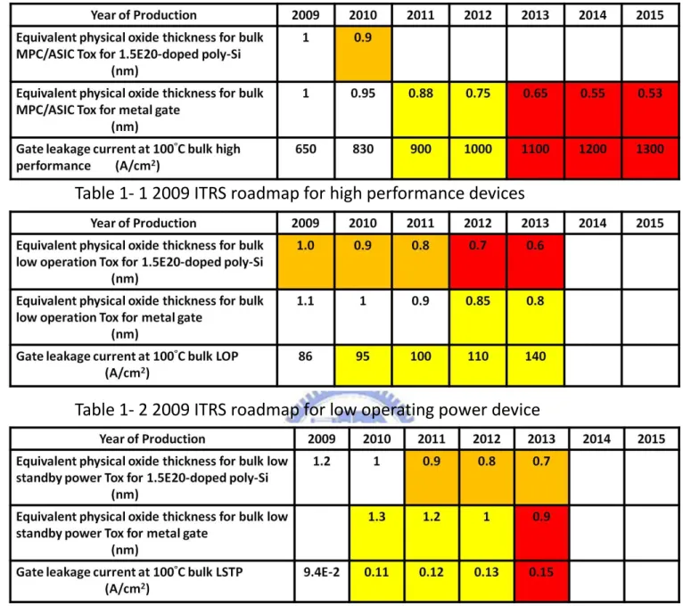
Table 1- 1 2009 ITRS roadmap for high performance devices ··· 13 Table 1- 2 2009 ITRS roadmap for low operating power device ··· 13 Table 1- 3 2009 ITRS roadmap for low standby power devices ··· 13
Chapter 03
Table. 3- 1 Conditions of samples with different passivation layers. ··· 34 Table. 3- 2 Electrical performance of samples with different passivation layers. ··· 43
Figure Captions
Chapter 01
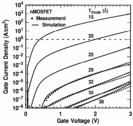
Fig .1- 1Measured and simulated Ig-Vg characteristics under inversion conditions of SiO2 nMOSFET devices. ··· 12
Fig .1- 2 Using high-k material can suppress gate direct-tunneling current. ··· 12
Chapter 02
Fig. 2- 1 Schematic representation of factors contributing to carrier mobility degradation in a high-k oxide layer. ··· 20 Fig. 2- 2 Measured effective electron mobility for HfSiON MISFETs and pure SiO2 MOSFETs as a function of effective field at 300-423K. Substrate concentration NA is
3 x 1016 cm-3. ··· 20 Fig. 2- 3 Hole constant-energy band surfaces for the top band obtained from six-band
k • p calculations for common types of 1-GPa stresses: (a) unstressed, (b) biaxial
tension, (c) longitudinal compression on (001) wafer, and (d) longitudinal compression on (110) wafer (note significant differences in stress induced band warping altering the effective mass). ··· 21 Fig. 2- 4 Summary of key valence-band parameters for top and second band for bulk Si under 500-MPa stress. The conductivity and density of states effective mass is listed at gamma point. Uniaxial compression is longitudinal along <110> channel
direction (note significant differences for in-plane, out-of-plane, and density-of-states masses). ··· 21 Fig. 2- 5 Conduction valley energy-level splitting under 500 MPa of longitudinal uniaxial tensile stress: Bulk and MOSFET inversion layer (1 MV/cm). Note that energy-level splitting from inversion-layer confinement is larger than strained. ··· 22 Fig. 2- 6 Simulated electron velocity along the channel of 0.1 um nMOSFET. ··· 22 Fig. 2- 7 Hot electrons and hot holes can be injected into oxide with the aid of vertical field, or with their own kinetic energy ··· 23 Fig. 2- 8 Fluorine repair the defect in gate and channel, and give the resistance to stress because of its strong binding energy. ··· 23
Chapter 03
Fig. 3- 1 The process flow of n-MOSFETs with different passivation layer. ··· 32 Fig. 3- 2 The PECVD system used in this experiment. ··· 33 Fig. 3- 3 Cross section of HfO2/SiON n-MOSFET with different passivation layer. 35 Fig. 3- 4 In FSG buffer P.L. devices, a large amount of F atoms incorporating to passivating the bulk and interface trap charges of HfO2/SiON gate stack n-MOSFET. ··· 35 Fig. 3- 5 The experimental setup for the basic electrical characteristics and long-term reliability test measurements. ··· 36
Fig. 3- 6 Basic measurement method for (a) CVS (constant voltage stress), and (b) HCI (hot carrier injection stress). ··· 37 Fig. 3- 7 HCI stress and relaxtion measurement method ··· 38 Fig. 3- 8 SIMS profiles shows that Fluorine diffuse into gate and channel ··· 39 Fig. 3- 9 XPS shows that after sintering, fluorine enhance Hf-O binding energy under Hf4f track ··· 39
Fig. 3- 10 XPS shows that fluorine diffuse into gate and channel, and some carbonized organic compounds. ··· 40 Fig. 3- 11 Gate leakage current as a function of gate voltages of HfO2/SiON gate stack with different passivation both under inversion and accumulation regions ··· 40 Fig. 3- 12 Drain current and transconductance as a function of gate voltages of HfO2/SiON gate stack with different passivation ··· 41 Fig. 3- 13 The maximum transconductance versus channel length for all splits of HfO2/SiON gate stack n-MOSFETs. ··· 41 Fig. 3- 14 Drain current versus drain voltage (ID-VD) curves of different P.L. under
various normalized gate biases which 0V, 0.375V, 0.75V, 1.125V, and 1.5V,respectively. ··· 42 Fig. 3- 15 Enhanced percentage of electrical performance of samples with different passivation layers ··· 43
Fig. 3- 17 Drain current degradation degree with different samples under CVS stress
··· 44
Fig. 3- 18 Vth shift degree with control sample under 100oC CVS ··· 45
Fig. 3- 19 Vth shift degree with SiN capping sample under 100oC CVS ··· 45
Fig. 3- 20 Vth shift degree with FSG buffer sample under 100oC CVS ··· 46
Fig. 3- 21 Substrate current versus gate voltage for both samples of HfO2/SiON gate stack n-MOSFETs. ··· 46
Fig. 3- 22 Vth shift degree under HCI stress for different samples at 25°C ··· 47
Fig. 3- 23 Drain current degradation degree with different samples under HCI stress 47 Fig. 3- 24 Comparison of ID,SAT as a function VGS of FSG buffer layer sample better than SiN capping sample and control sample ··· 48
Fig. 3- 25 Comparison of TBD lifetime projection as a function VGS of FSG buffer layer sample larger than SiN capping sample and control sample ··· 48
Fig. 3- 26 Threshold voltage shift with de-trapping bias –2 V dependence after hot carrier stress on both samples. ··· 49
Fig. 3- 27 Schematic explanation of stress and relaxation process with different bias conditions for (a) Control (b) SiN capping (c)FSG buffer samples ··· 50
Chapter 1
Introduction
1.1 Background
Recnetly, CMOS devices have been aggressively scaled into sub-45 nm regime in order to enhance the device’s performance and increase the integrated circuit functionally, scaling down of the channel length is essential in ULSI fabrication technologies [1-2]. With this scaling down, the gate oxide thickness of MOSFETs must be reduced. The main scalling issues in the advanced CMOS devices in the sub-100 nm regime is the thinning of gate oxide that is required for higher drive current and to improve the gate control over the channel, which reduces the short channel effects [3-4]. According to the ITRS (International Technology Roadmap for Semiconductor) roadmap (Table 1-1) [5], the SiO2 gate dielectric film thickness
should be scaled down to 1.0nm for 45nm node technology. Such an ultra-thin SiO2
thin film consists of only a few atomic layers will cause an intolerable large gate leakage current because of direct tunneling effect, and this will result in huge power dissipation and heat which let the integrated device can not work regularly.
leakage current will exponentially increase, Figure. 1-1 demonstrated the measured and simulated Ig-Vg characteristics under inversion region for nMOSFET [6]. We can
see that the gate leakage current will exceed the limit of 1 A/cm2 set by the allowable power dissipation Pleakage=Ileakage*Vdd (Ileakage=Igate+Ids_sub+IBTBT) while the gate oxide
thickness scaled down to 2 nm. We need a new materials such as high-k materials to reduce the tunneling leakage current (i.e suppressing gate oxide leakage and subthreshold leakage current) [7-8]. And when the using of high-k materials, metal electrodes are needed due to their better comparability with high-k dielectrics and absence of the depletion effect. According to the ITRS and the future trends, replacing polysilicon by metal gates is critical.
According to the first order current-voltage relation in Equation (1-1) and (1-2), the driving current of a MOSFET can be given as:
(1-1)
(1-2)
Where VGS is the applied voltage from gate to source, Leff is the effective
channel length, W is the channel width, Vth is the threshold voltage, μn is the mobility
for electrons, Cgs is the gate capacitance, k is the dielectric constant, ε0 is the
permittivity of free space and Tinv is the electrical film thickness. In an attempt to
formula can be appropriatly adjusted. With reduced threshold voltage, smaller effective channel length, and increased gate capacitance as well as gate-to-source voltage, we can achieve better current drivability and higher device density, which means better performance and much more transistors on the chip, respectively. However, some approaches will bring about serious drawbacks, for instance, a large VGS will degrade the reliability while too small a Vth will result in statistical
fluctuation in thermal energy at a typical operation circumstance of up to 100°C. So bigger Cgs , μn and shorter Leff will be needed to maintain device performance. In
the front-end process area, there remain many technological challenges to be overcome to achieve further scaling and growth of the industry [9]:
New gate stack processes and Materials Surfaces and interfaces control
CMOS integration of new memory materials and processes Critical dimension and effective channel length control Scaled MOSFET dopant introduction and control
1.2 Motivation
SiO2 gate dielectric and polysilicon gate have been used as perfect materials
deep sub-micron regime, SiO2 used as gate oxide is facing serious challenges which
seem to be almost impossible to overcome such as leakage current problem proposed by previous section. In addition, reliability issues and process stability become a serious concern for such a thin SiO2 thickness only 10~15A. It points out that SiO2
thickness uniformity across a 12 inch wafer imposes even more crucial difficulty in the growth of such a thin film, since even a mono-layer difference in thickness represents a large percentage difference and thus can result in the variation of electrical characteristics such as threshold voltage (Vth) across the whole wafer. To
circumvent these problems, high-k dielectrics have been investigated extensively as possible replacement to the SiO2 film as gate insulators. Using gate dielectrics with
higher dielectric, electrically equivalent oxide thickness (EOT) in order to maintain the same gate capacitance can be obtained with a thicker physical thickness. Therefore, the quantum direct tunneling gate leakage current can be significantly reduced (shown in Fig. 1-2).
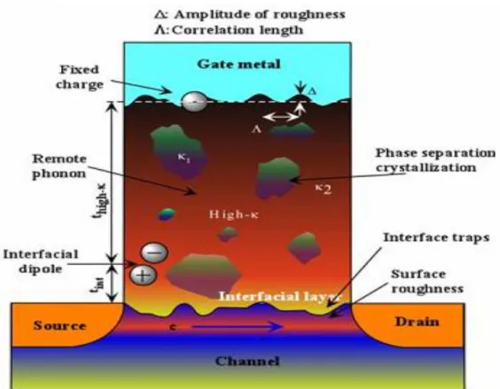
Nevertheless, there are still various problems to be solved for high-k gate dielectrics before their use in IC technology. First, the poor interface with Si is commonly observed [10]. The high-k oxides are deposited on the surface of Si and thus do not passivate its interface. This results in a large number of interface traps and charges which is detrimental to metal-oxide-semiconductor (MOS) device
performance such as flat band voltage shift and mobility degradation [11-12]. Originally we used new high-k materials to make capacitance Cgs increases which
enhance driving current, but degrade the mobility μn , results in the enhanced degree
is not as high as we think before. In order to further enhance the driving current, we investigate the effect of adding locally strain technology on high-k gate stack nMOSFETs.
1.3 Recent locally strain technology
In recent years, the method of device size-scaling to enhance the MOS transistor performance characteristics seems to encounter bottlenecks in lithography process technology such as high cost and other factors. People began to seek other ways, and one method used to improve device driving current has been concerned, that is strain-Si technology. Development so far, excluding the impact of high-k materials, uniaxial-process-induced stress strain-Si technology is the key feature to enhance 90-, 65-, and 45-nm [13-20].
The origin of strained-Si technology to improve CMOS devices can be traced to thin Si/SiGe substrates at 1980s [21-22]. The thin Si layer takes the larger lattice constant of the SiGe and creates biaxial tensile stress. Then wafer-based substrate strain was experimentally and theoretically studied by a large number of researchers
for two decades [23]. In the 1990s, two other strained-Si technologies based on process-induced strain were developed. First, high-stress capping layers deposited on MOSFETs were investigated as a technique to introduce stress into the channel [24-25]. Second, Gannavaram et al. [26] proposed SiGe in the source and drain area for higher boron activation and reduced external resistance. It was later attributed to uniaxial compressive channel stress [27]. Still, neither biaxial nor uniaxial stress was immediately adopted in CMOS logic technologies for several reasons. Biaxial stress suffers from defects and performance loss at high vertical electric fields [28]. Process-induced stress requires different stress types (compressive and tensile for n- and p-channel, respectively) to simultaneously improve both n- and p-channel devices. However, in the industry, strain was becoming recognized as offering the best potential to enhance performance in sub-100-nm process technologies (significantly larger performance gain than high-k gates, fully depleted silicon-on-insulator (SOI), or multi-gate devices). The only debate was on the best path to take [29] (biaxial substrate versus uniaxial-process-induced stress).
Careful analysis of the 1990’s biaxial and uniaxial strained-Si experimental data suggested that the industry adopt process induced uniaxial strain. The key observations are as follows. First, uniaxial (versus biaxial) stress provides significantly larger hole mobility enhancement at both low strain and high vertical
electric field due to differences in the warping of the valence band under strain [30]. Large mobility enhancement at low strain is important since yield loss via dislocations occurs at high strain. Second, uniaxial (versus biaxial) stress enhanced mobility provides larger drive current improvement for nanoscale short-channel devices. This results since the uniaxial stress-enhanced electron and hole mobility arises mostly from reduced conductivity effective mass (versus reduced scattering for biaxial stress), since uniaxial shear stress provides significant valence and some conduction band warping.
With these advantages for process-induced uniaxial strain understood. Two process flows were developed that independently target the stress magnitude and direction on n- and p-channel transistors. The first involved embedded and raised SiGe in the p-channel source and drain and a tensile capping layer on the n-channel device. The second uses dual stress liners: compressive and tensile Silicon Nitride (SiN) for p- and n-channel devices, respectively. Since both techniques provide large product level benefits at low cost, process-induced stress is present in nearly all high-performance logic technologies at the 90-, 65-, and 45-nm technology nodes for both microprocessor and consumer products. The industry is now looking at combining various process stressors, such as compressive SiN layers, embedded SiGe, and tensile stress shallow-trench isolation [31]. Performance gains from the various
uniaxial stressors are expected to be mostly additive.
1.4 Enhancing Robustness by Fluorine
Traditionally we use silicon oxide as the insulator of CMOS because of its excellent stablility , but it normally has few defects. At Si/SiO2 interfaces, the defect density is further lowered by hydrogenation during process , with any Si dangling bonds Pb centers converted to Si–H bonds. Historically the appropriately incorporation of the fluorine into gate dielectric is known as an effective way to passivate the interface traps in the conventional SiO2 gate dielectric and can improve device reliability because it was known that fluorine incorporation in the SiO2 gate dielectrics replaces Si–H bonds with Si–F bonds, Si-F bonds are rather strong than Si-H bonds. But the high-k oxides itself exist more much bulk trap charges than silicon oxide and suffer from a high density of charge traps. This phenomenom causes temporary instability of the gate threshold voltage, carrier coulombic scattering in the Si channel, and possible reliability problems. Recent work indicates that the main charge trap is the oxygen vacancy VO [32]. The high-k oxides differ from Si-H bonds
or Si-O bonds , they all have ionic bonding. As a result of implanted fluorine that was found to have a large beneficial effect on charge trapping [33-35], F was found to substitute at the VO site and passivates it. And F is one of the best passivate element
for defects in an ionic oxide because it is the only element that is more electronegative than oxygen and its bond length is similar. It can improve both the device performance and reliability by passivated vacancies by F inionic oxides such as HfO2
because vacancies are more likely to be charged. However, an excess amount of F incorporation increases oxidethickness and could weaken the isolation of capacitance oxide of nMOSFET. It is known that excessive F replaces Si–O bonds with Si–F bonds when annealing, which generates reactive oxygen atoms and probably diffuse into channel. The oxygen atoms which react with silicon substrate, will form thicker interfacial SiOx layer. Moreover, another drawback after an excess amount of fluorination is a net negative charge which affect the drifting of electrons existed at the high-k oxide and interfacial layer , they also increasing the leakage current density [35]. The impurities exists in isolation oxide layer will possibly make barrier height lowering or become Frenkel-Poole transport sites for electron transport through the high-k oxide stacks result in higher leakage current, this will lose the original purpose of using high-k dielectrics. Previous work studies suggest an insight into this problem. It was observed that the concentration of interstitial F ions was reduced by two orders of magnitude after a 400 °C FGA. Hydrogen annealings seem to be able to remove excess F ions which are not strongly bonded in the bulk region of the HfO2 films [35].
It is beyond doubt that appropiately concerntration adding fluorine will enhance electrical performance and reliability, adding the F element at the HfO2/SiO2 interface may be an essential aspect of such a defect passivation scheme. When we use strain-Si technology for enhancing driving current, leakage current and defect density increases too, adding fluorine will be the most effective candidate to eliminate these phenomenons even if its disadvantages. At the following experiment, we try to prove the application of fluorine.
1.5 Organization of This Thesis
In this thesis. We bring up the new process to enhance the strain engineering. We discuss the effects of fluorine incorporation into the passivation of strained-si HfO2/SiON gate stack n-MOSFETs, evaluated in terms of reliability and
performances. In this chapter, we introduce the reason of the high-k dielectrics and the strain engineering on CMOS technology and discuss the effects of fluorine incorporating on MOSFETs with strained-Si high-k gate dielectric stacks, this thesis is organized as follows:
In chapter 02, we discuss the theoretical characteristics of strained-Si technology. Besides, hot carrier reliability is also discussed.
HfO2/SiON gate stack nMOSFETs test devices withdifferent passivation.Then, show
basic electrical performance, i.e. I-V characteristics, and presents the effects of FSG passivation dielectric on strained-Si HfO2 n-MOSFET reliability.
In chapter 04, we bring up conclusions for these experimental results above . Some advices for the possible future researches are suggested in this area.
Fig .1- 1Measured and simulated Ig-Vg characteristics under inversion conditions of SiO2 nMOSFET devices.
Table 1- 1 2009 ITRS roadmap for high performance devices
Table 1- 2 2009 ITRS roadmap for low operating power device
Chapter 2
Local strained-Si on HfO
2/SiON nMOSFETs
2.1 Mobility degradation by high-k materials
In the future, High-K insulators will be utilized as gate dielectric films for advanced CMOS devices. But one of main problems of the high-K MOSFETs is reduced carrier mobility compared with that of thermally grown pure SiO2 MOSFETs because of the uncompleteness on high-k film itself (see Fig. 2-1). The research reveal that the electron mobility degradation for HfSiON MOSFETs [36] (see Fig. 2-2) and find that two sources of the mobility degradation: one is Coulomb scattering caused by fixed charges in High-k films and the other is phonon scattering by interfacial thin oxynitrided (SiON) layer.
2.2 Mobility enhanced by local strained-si
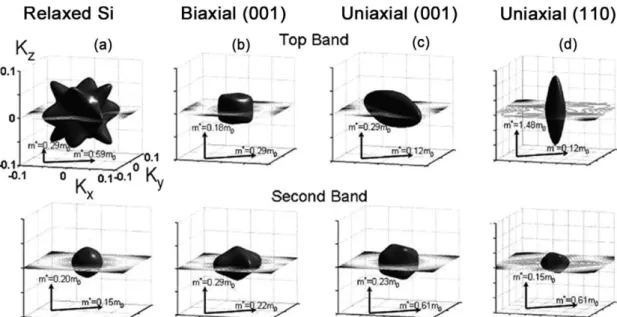
In order to improve the degradation mobility caused by High-k gate stacks, strained-Si are required to improve drive current. When deciding on a strained-Si process flow, it is first necessary to comprehend the potential magnitude for electron versus hole mobility enhancement and whether the mobility enhancement results from
relationship for semiconductors depends on nearest neighbor atomic spacing, certain stress (in particular shear stress) warps the valence bands (although less so for conduction band but some warping for shear stress) [38]. The warping of the valence band provides dramatic changes to the constant-energy surfaces in k space and can lead to large hole mobility enhancement via reduced conductivity mass in the channel direction. Mobility enhancement via reduced mass (as opposed to reduced scattering) is key in nanoscale MOSFETs and often not appreciated. Only mobility enhancement from reduced mass (unlike reduced scattering) is maintained at the very short 15–20-nm channel lengths (35-nm gate length) devices currently in production. A strained-Si flow, which is scalable for multiple technology nodes, thus, needs to focus on reducing the hole conductivity mass with the goal of improving the n/p ratio from ~2 to ~1. Therefore, we first focus on strain-enhanced hole mobility from reduced conductivity mass. As a starting point, it is helpful to visualize the effect of strain on the valence-band constant-energy surfaces in k space for bulk Si. Fig. 2-3 [37] shows the surfaces obtained using six band k • p and band parameters in [39]. The strain-altered surfaces for the top two bands are shown at 1 GPa for the common stresses of interest: longitudinal compression on (001) and (110) hybrid wafer orientation and biaxial tensile stress. Note from the constant-energy surfaces in Fig. 2-3, the heavy and light hole bands lose their meaning and we label the bands (first,
second, etc.) in this paper. Some important differences in the band structure under the various stresses at 500 MPa are summarized in Fig. 2-4 [37] for the in-plane and out-of-plane conductivity effective masses and density of states at the band edge. Before covering strain-altered hole mobility calculations, we will briefly cover a qualitative model for strained-enhanced electron mobility since the concepts are similar for electrons and holes.The electron mobility in bulk strained- Si along <110> direction is determined by occupation and scattering in the Δ2 and Δ4 valleys and can
be expressed as:
where q, n, τ , and m are the electron charge, concentration, relaxation time, and conductivity mass in the MOSFET channel direction, respectively. Strain improves the mobility by increasing the electron concentration in the Δ2 valley. The
repopulation improves the average in-plane conductivity mass (unstressed: mt =
0.19m0 versus ml = 0.98m0) and some further improvement is possible for stresses that
warp the conduction valleys and lower mt [38].Reduced intervalley scattering by the
strain-induced splitting between Δ2 and Δ4 plays some role (enhances long channel
mobility) when the splitting becomes comparable or larger than the optical phonon energy. In addition to a low in-plane mass, a high out-of-plane mass for the Δ2 valley
(taken as the z-direction in this paper) is quantized. This quantization in addition to strain alters the position of the energy levels. The quantization leads to bands becoming subbands since only discrete wave vectors kz are allowed. Including
quantization, the total inversion-layer electron energy is given by discrete values of energy (En) added to the electron energy in the x- and y-directions (in the plane of the
MOSFET) [40]
Each step in energy is called a subband with En the energy of the bottom of the
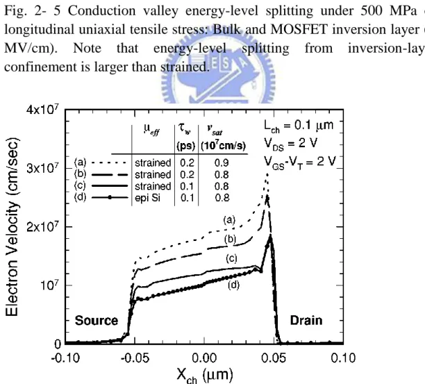
subband. As an example, self-consistent solution of Schrödinger and Poisson equation for 500 MPa of uniaxial tensile stress and an inversion-layer vertical field of 1 MV/cm gives the energy levels, as shown in Fig. 2-5 [37]. Since the subband separation is greater than kT, nearly all the electrons in most cases occupy the bottom two subbands [ground state n = 0 typically called Eo (from Δ2) and Eo’ (from Δ4)]. The
ground state energy is significantly lower for the Δ2 valleys because of the higher
quantization mass (Δ2: mz = 0.98m0 versus Δ4: mz = 0.19m0) which leads to increased
splitting between the bottom two subbands and confinement and strain splitting being additive (for the common biaxial and uniaxial tensile stress). The strong confinement in an MOSFET shifts the energy levels more than the moderate 500-MPa stress
mass in the bottom subband (top subband for holes) is an important requirement for the strainaltered band structure. Lastly, in addition to a low in-plane and high out-of-plane effective mass, a high in-plane mass perpendicular to the channel direction is also important. The density of states per unit area for the quantized system is , which results in the density-of-states mass approximated by . Though strain does not significantly alter the electron subband density of states, as discussed next, a high will be shown to be important for maintaining a hole concentration in the top subband. Similar to strained-enhanced electron mobility, hole mobility in an inversion layer can qualitatively be described as resulting from occupation and scattering in the top two bands
However, hole transport is more complicated since strain significantly warps the valence band (as seen in Fig. 2-3) altering both the in- and out-of-plane mass and
. Further, the mass changes with stress and is not constant in k space. After the
previous discussion on strain-enhanced electron transport, an advantageous strain for holes needs to warp the valence band to create both a low in-plane and high out-of-plane mass and, if possible, a large mass in the plane of the MOSFET
perpendicular to the channel direction (creates a large ).
2.3 Local strained-si induced Serious hot carrier injection
phenomenon
We had discussed that strain-si can enhance the device mobility described as above, but it will create serious hot carrier injection. Fig 2-6 demonstrated that after added strain-si technology, enhance si-channel mobility and enhance the electron velocity near drain site, then give electron more energy, and will induce high probability to impact ionize (see Fig 2-7), results in serious hot carrier injection.
At chapter one, we had discussed that incorporating fluorine can give resistence to hot carrier (see Fig 2-8), so now we design a new experiment that we can enhance mobility and reduce the serious HCI effect by incorporated fluorine into strained-Si High-k gate stack devices.
Fig. 2- 1 Schematic representation of factors contributing to carrier
mobility degradation in a high-k oxide layer.
Fig. 2- 2 Measured effective electron mobility for HfSiON MISFETs and
pure SiO2 MOSFETs as a function of effective field at 300-423K.
Substrate concentration N
Ais 3 x 10
16
Fig. 2- 3 Hole constant-energy band surfaces for the top band obtained from six-band
k • p calculations for common types of 1-GPa stresses: (a) unstressed, (b) biaxial
tension, (c) longitudinal compression on (001) wafer, and (d) longitudinal compression on (110) wafer (note significant differences in stress induced band warping altering the effective mass).
Fig. 2- 4 Summary of key valence-band parameters for top and second
band for bulk Si under 500-MPa stress. The conductivity and density of
states effective mass is listed at gamma point. Uniaxial compression is
longitudinal along <110> channel direction (note significant differences
for in-plane, out-of-plane, and density-of-states masses).
Fig. 2- 5 Conduction valley energy-level splitting under 500 MPa of
longitudinal uniaxial tensile stress: Bulk and MOSFET inversion layer (1
MV/cm). Note that energy-level splitting from inversion-layer
confinement is larger than strained.
Fig. 2- 6 Simulated electron velocity along the channel of 0.1 um
nMOSFET.
Fig. 2- 7 Hot electrons and hot holes can be injected into oxide with the
aid of vertical field, or with their own kinetic energy
Fig. 2- 8 Fluorine repair the defect in gate and channel, and give the
resistance to stress because of its strong binding energy.
Chapter 3
Experimetal Result and discussion of Local
strained-Si HfO2/SiON nMOSFETs with FSG
passivation layer
3.1 Experiment
This experiment construct simple HfO2/SiON gate stack nMOSFETs with SiO2
passivation layer deposited by TEOS source liquid for control, and with Nitride passivation layer for local strained-Si effect, and Nitride passivation layer with added FSG passivation layer on underside for Fluorine incorporated effect.
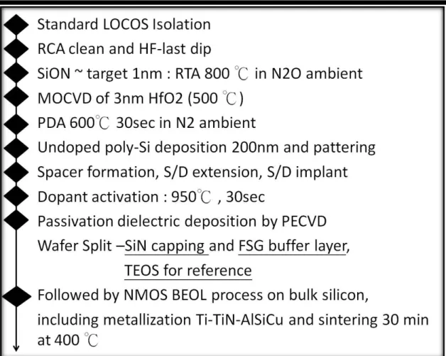
Fig.3-1 shows the experimental process flow of the nMOSFET with HfO2/SiON gate dielectric. The nMOSFETs were fabricated on 6-inch p-type (100) Czochralski (CZ) silicon (Si) wafer utilizing a conventional self-align process, followed by the standard RCA cleaning with a hydrofluoric (HF) acid-last process. Prior to the HfO2 gate dielectric deposition, less than 1 nm interfacial SiON was grown by rapid thermal processing in the nitrous oxide (N2O) ambient at 800°C for 30
s. The 3 nm HfO2 gate dielectric was subsequently deposited by the AIXTRON metal organic chemical vapor deposition system at 500°C, followed by post deposition
200 nm poly- Si gate was then deposited by low-pressure chemical vapor deposition system using silane (SiH4) gas at 620°C. After gate electrode patterning by I-line
lithography stepper and subsequently phosphorous implantation at 20 keV, 5 x1015 cm2 dose, dopants were then activated at 950°C for 30 s in N2 ambient. Afterward,
wafer split into SiN capping, FSG buffer layer and control samples by varied passivation layer , and all passivation layer deposited using the plasma-enhanced chemical vapor deposition (PECVD) (see Fig. 3-2) system at 300°C. SiN capping sample deposited 300nm nitride and 100nm SiO2, FSG buffer layer sample deposited 20nm FSG ,300nm nitride and 100nm SiO2 , and control sample deposited 400nm for reference (see Table 2-1). Nitride passivation layer was deposited at the SiH4 , NH3,
N2 ; FSG passivation layer was deposited at the SiH4, N2O and CF4, and undoped
SiO2 passivation layer was deposited at the O2 and TEOS source gas. Varied
passivation was used to investigate the effect of incorporated fluorine on local strain-Si HfO2/SiON device performances. Finally, contact holes etching and
metallization Ti-TiN-AlSiCu were performed using standard CMOS process, followed by 400°C sintering for 30 min in N2 ambient. Fig 3-3 illustrate schematic
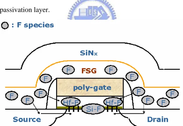
cross section of HfO2/SiON n-MOSFETs with different passivation layer. Fig 3-4 illustrate F atoms diffuse into channel after sintering.
3.2 Measurement setup
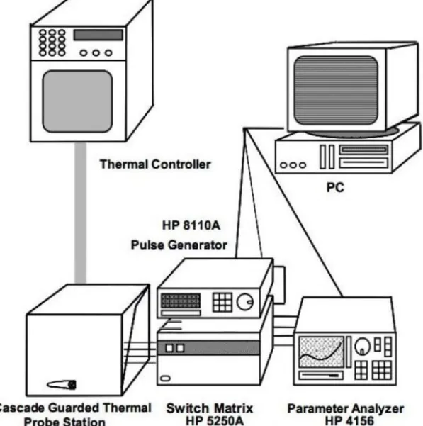
Basic electrical characteristic such as I-V were measured by a HP4156A precision semiconductor parameter analyzer (see Fig 3-5).
In CVS reliability at room temperature and 100oC measurements, devices were stressed with the drain voltage set at 0.1 voltage, and the gate voltage biased at threshold voltage plus 3 voltage, and monitor the constant voltage degradation before and after stress. To find the condition, we first measured the ID –VGS characteristics with drain terminal was biased at the 0.1 voltage, and voltage found by current defined method (see Fig 3-6a).
In HCS reliability at room temperature and 100oC measurements, devices were stressed with the drain voltage set at a highly positive voltage, and the gate terminal was biased at the voltage where maximum absolute value of Isub occurred to accelerate the degradation. To find the condition, we first measured the Isub –VGS characteristics with drain terminal biased at a given voltage. Besides, In order to identify the worst degradation condition, VGS = VGS@Isubmax (channel hot electron, CHE) was used to monitor the degradations of our devices for hot electron stressing. To monitor the hot electron degradation, both the ID –VGS characteristics at VDS = 0.1V (linear region) and damages were monitored before and after the stress. The degradations in terms of threshold voltage shift (△Vth) were examined and recorded in
the accelerated stress test (see Fig 3-6b).
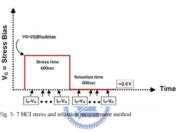
Additionally, in order to monitor the charge de-trapping effect, we set HCI stress/relaxtion with a 600 seconds HCI stress described as above and 600 seconds relaxtion voltage VGS=-2V, and 600 seconds HCI stress again to mention threshold voltage shift (see Fig 3-7).
3.3 Result and discussion
3.3.1 Electrical characteristics of high-k gate stack
nMOSFETs with different P.L.
At Fig. 3-8, the SIMS profile shows that the Fluorine concerntration at gate higher than at HfO2/Si-channel interface, this means fluorine diffuses into gate and
channel, and at Fig 3-9, from Hf track we can see that after fluorine diffused into gate, Hf-O binding energy become higher, at Fig 3-10, from F track we can see at 684eV binding energy has high peak shows that fluorine is indeed diffuse into gate and channel, and at 689eV has a small peak shows that because of the source gas of FSG buffer layer is CF4, carbon also diffuse into gate and channel and form some organic
compounds. Fig. 3-11 shows the gate leakage current of HfO2/SiON gate stack n-MOSFET with different passivation under both inversion and accumulation modes. It can obviously noted that with FSG buffer passivation layer and SiN capping
passivation layer because of Fluorine and Nitrogen passivate the defect at High-k gate, the leakage current is significantly suppressed. Fig.3-12 demonstrates the transconductance (Gm) and the linear region drain current as a function of gate voltage for different samples. The peak transconductance is 6.6%, 21.5% for SiN capping and FSG buffer samples respect to control sample, and the improved normalized linear drain–current ID which SiN capping sample is 9.8% higher above
than control samples and the FSG buffer sample is 22.9% higher than control samples, indicating that fluorinated strained-si HfO2 has better interface characterization. Fig. 3-14 presents the excellent output drive current characteristics (ID-VDS) under various
normalized gate biases (VGS-VTH), which almost 12% enhancement in magnitude of
ID,SAT for FSG buffer sample with respect to control sample. The improvements are
believed to be intimately related not only to the better interface quality but also to the reduced bulk trap density. Fig 3-13 indicates the transconductance of devices with different passivation layers as a function of channel length. And we find that transconductance for FSG buffer sample shows the better interface states than SiN sample and control sample. Thus, the strain-si technology will improve the transconductance in device, and FSG buffer layer can further improve it. In short, Table 3-2 and Fig 3-15 demonstrate that all fundamental electrical properties, including the threshold voltage, linear region drive current, saturation region drive
current, transconductance, swing, gate leakage current between the three splits with control, SiN capping and FSG buffer layer samples. We can see that local strain technology can improve electrical performance, and added FSG buffer layer can further improve them.
3.3.2 Reliability characteristics of high-k gate stack
nMOSFETs with different P.L.
First, we focus on reliability characteristics of HfO2/SiON gate stack n-MOSFETs with different samples under constant DC stress condition. Fig. 3-16 and Fig. 3-17 compares the threshold voltage and ID,lin variations as a function of stress
time for the different samples, respevtively. Fig. 3-18~20 shows the 100oC CVS with control, SiN capping, FSG buffer samples, respectively. We can see that compared to control sample, SiN capping sample have more resistance to CVS under 25oC and 100oC, and FSG buffer layer sample have advanced resistance compared to SiN capping sample. It is beleived that damage under CVS stress mainly comes from High-k bulk defect, so now we know when we only capping SiN, nitrogen can passivate the bulk defect; when we use FSG buffer, and the fluorine can passivate the bulk defect.
strain-si induced more impact iozination, and they cause more Isub.Fig. 3-22 and Fig.
3-23 compares the threshold voltage and ID,lin variations as a function of HCI stress
time for the different samples, respevtively. We can see that SiN capping sample suffer serious HCI damage than control sample, and FSG buffer sample can enhance HCI stress resistence under strain-si technology. It is beleived that damage under HCI stress mainly comes from High-k/Si-channel interface state, so now we know when we only capping SiN, hydrogen will passivate the bulk defect, but easily be damaged under stress, and when we use FSG buffer, this FSG buffer layer prevent the following hydrogen diffusing, and the fluorine can passivate the interface state defect.
Third, we discuss the ten year using straight line, Fig. 3-24 and Fig 3-25 shows added FSG buffer sample has better ID,SAT and Time-to-breakdown profiles
Fourth, we discuss the voltage shift and relaxation under HCI stress, Fig 3-26 shows the results, and Fig 3-27(a-c) shows the mechanism with control sample, SiN capping sample, FSG buffer sample, respectively. Compared to control sample, SiN capping sample has more defect and release less electrons under relaxation phase, and FSG buffer sample can has less defect and release less electrons.
Now the experimental results reveal that the fluorine incorporated by FSG buffer layer can enhance the reliability. Because when fluorine diffuse into gate bulk and channel interface (shown in Fig. 3-28), they can form Si-F and Hf-F bonds, and
these bonds has strong binding energy, can give the resistence to CVS and HCI stress.
3.4 Summary
In this work, we show the experimental electrical properties of the devices with different passivation layer, significant device performance improvement in devices with FSG buffer P.L. were found, such as the excellent subthreshold swing, increased transconductance, higher current drive, as compared to the control TEOS sample and SiN capping sample. It was observed that incorporated fluorine can repair the defects under the local strain-Si technology, further improve the device performance.
And we also observe that serious degradation such as interface state trap, bulk trap density result in threshold voltage shift occurs in the control sample. The CF4-introduced silicon oxide as a FSG buffer layer showed that improved reliability characteristics under the CVS and HCI. It is believed that the CVS and HCI degradation are related to the electron traps in gate dielectrics. As compared to the control sample, the SiN capping sample suffer serious hot carrier injection, and The FSG buffer layer sample leading to the formation of stronger Hf-F and Si-F bonds compared to Hf-H and Si-H bonds reduced charge trap generation rate. These stronger bonds result in less interface states generation and charge trapping under CVS and HCS, which promotes better hot-carrier and CVS immunity against stress.
Fig. 3- 1 The process flow of n-MOSFETs with different
passivation layer.
Table. 3- 1 Conditions of samples with different passivation
layers.
SiO2: 300sccm O2, 50sccm TEOS, 500mTorr, 40W, 300oC
NITRIDE: 20sccm SiH4, 20sccm NH3, 980sccm N2, 850mTorr, 20W, 300oC
FSG: 5sccm SiH4, 90sccm N2O, 20sccm CF4, 1Torr, 11W, 300oC
3000A NITRIDE stress degree: 3.366x10² MPa Tensile stress
Fig. 3- 3 Cross section of HfO2/SiON n-MOSFET with different
passivation layer.
Fig. 3- 4 In FSG buffer P.L. devices, a large amount of F atoms
incorporating to passivating the bulk and interface trap charges
Fig. 3- 5 The experimental setup for the basic electrical
characteristics and long-term reliability test measurements.
Fig. 3- 6 Basic measurement method for (a) CVS (constant
voltage stress), and (b) HCI (hot carrier injection stress).
n+ n+ n+ P G ID-VG DC stress 10sec ….. ID-VG: To evaluate △Vth ID-VG ID-VG ID-VG DC stress 5sec DC stress 1sec
CVS for gate electrode CVS: VGS=Vth+3V Change T T=25、100oC n+ n+ n+ P G ID-VG DC stress 10sec ….. ID-VG: To evaluate △Vth ID-VG ID-VG ID-VG DC stress 5sec DC stress 1sec
HCI for gate electrode HCI:VGS=VGS@Isubmax VDS=3V
Change T
0 5 10 15 20 25 30 103 104 105 106 Si-sub In te n s (C /S ) Depth(nm) Fluorine Silicon Oxygen Hafnium HfO2
Fig. 3- 8 SIMS profiles shows that Fluorine diffuse into gate and channel
21 20 19 18 17 16 15 14 13
(b) 16.52
Binding Energy (eV)
In te n si ty ( a r b . u n it ) 16.14 (a) 21 20 19 18 17 16 15 14 13 (a) w/o Fluorined
(b) Fluorined
Hf4f of the HfO2
Fig. 3- 9 XPS shows that after sintering, fluorine enhance Hf-O binding
energy under Hf
4ftrack
680 682 684 686 688 690 F 1S of the HfO2 In te n s it y ( a rb . u n it )
Binding Energy (eV)
Fig. 3- 10 XPS shows that fluorine diffuse into gate and channel, and
some carbonized organic compounds.
-7 -6 -5 -4 -3 -2 -1 0 1 2 3 4 5 6 7
10-13 10-12 10-11 10-10 10-9 10-8 10-7 10-6 10-5 10-4 10-3L/W=0.5/10
Control
SiN Capping
FSG buffer layer
G
a
te
l
e
a
k
a
g
e
c
u
rr
e
n
t
(A
)
Gate voltage (V)
Fig. 3- 11 Gate leakage current as a function of gate voltages of
HfO2/SiON gate stack with different passivation both under inversion
and accumulation regions
-0.4 -0.2 0.0 0.2 0.4 0.6 0.8 1.0 1.2 1.4
0
50
100
150
200
250
0
40
80
120
160
200
240
280
21.5% T ra n s c o n d u c ta n c e(
S)
V
G-V
TH(V)
6.6%Control
FSG buffer layer
SiN capping
22.9% 9.8% D ra in c u rr e n t(
A)
L/W=0.4/10
V
DS=0.1V
Fig. 3- 12 Drain current and transconductance as a function of gate
voltages of HfO2/SiON gate stack with different passivation
0.2 0.4 0.6 0.8 1.0 1.2 100 150 200 250 300 350 400
GM
M a x(
S
)
Channel Length(um) Contol SiN capping FSG buffer layerFig. 3- 13 The maximum transconductance versus channel length for all
splits of HfO2/SiON gate stack n-MOSFETs.
Fig. 3- 14 Drain current versus drain voltage (I
D-V
D) curves of different
P.L. under various normalized gate biases which 0V, 0.375V, 0.75V,
1.125V, and 1.5V,respectively.
0.0 0.5 1.0 1.5 2.0 2.5 3.00.0
0.2
0.4
0.6
0.8
1.0
1.2
1.4
1.6
1.8
2.0
2.2
28.7% 23.3%Control
SiN capping
FSG buffer layer
W/L=0.4/10
D
ra
in
C
u
rr
e
n
t
(m
A
)
Drain Voltage (V)
V
G-V
TH=0~1.5V
Step=0.375V
Table. 3- 2 Electrical performance of samples with different passivation
layers.
Fig. 3- 15 Enhanced percentage of electrical performance of samples with
different passivation layers
0 5 10 15 20 25 30
SiN capping FSG buffer
Enh
anced
p
er
cen
tag
e(%)
S.S. GMmax Id,lin Id,sat0
200
400
600
800
1000
0
50
100
150
200
250
300
350
400
Control
SiN Capping
FSG buffer layer
T
h
re
sh
o
ld
v
o
lt
ag
e
sh
if
t
(m
V
)
Stress time (sec)
L/W=0.4/10
V
G-V
TH=3V
Fig. 3- 16 Vth shift degree under CVS stress for different samples at
25°C
1 10 100 1000 1 10ID
,l
in
D
e
g
ra
d
a
ti
o
n
[
%
]
Stress Time (sec)
Control
SiN capping
FSG buffer layer
L/W=0.4/10
Temp=25
oC
V
G-V
TH=3V
Fig. 3- 17 Drain current degradation degree with different samples under
CVS stress
0 1 2 1E-12 1E-11 1E-10 1E-9 1E-8 1E-7 1E-6 1E-5 1E-4 0 1 2 1E-14 1E-13 1E-12 1E-11 1E-10 1E-9 1E-8 1E-7 1E-6 1E-5 Gate Voltage(V) D ra in c u rr e n t( A ) L/W=0.4/10 Temp.=100o C VGS-VTH =3.0V T=0s T=1000s Control
D
ra
in
c
u
rr
e
n
t(
A
)
Gate Voltage(V)
T=25
oC
Vth Shift
Fig. 3- 18 Vth shift degree with control sample under 100
oC CVS
0 1 2 1E-7 1E-6 1E-5 1E-4
Vth Shift
T=25
oC
0 1 2 1E-9 1E-8 1E-7 1E-6 1E-5 1E-4 Gate Voltage(V) D ra in c u rr e n t( A ) L/W=0.4/10 Temp.=100oC VGS-VTH =3.0V T=0s T=1000s SiN cappingD
ra
in
c
u
rr
e
n
t(
A
)
Gate Voltage(V)
0 1 2 1E-8 1E-7 1E-6 1E-5 1E-4
Vth Shift
T=25
oC
0 1 2 1E-10 1E-9 1E-8 1E-7 1E-6 1E-5 1E-4 D ra in c u rr e n t( A ) Gate Voltage(V) L/W=0.4/10 Temp.=100oC VGS-VTH =3.0V T=0s T=1000s FSG bufferD
ra
in
c
u
rr
e
n
t(
A
)
Gate Voltage(V)
Fig. 3- 20 Vth shift degree with FSG buffer sample under 100
oC CVS
1.4
1.6
1.8
2.0
2.2
2.4
2.6
2.8
3.0
0
1
2
3
4
5
6
7
8
L/W=0.3/10
V
DS=3V V
G@I
Sub MaxControl
FSG buffer layer
SiN capping
S
u
b
s
tr
a
te
c
u
rr
e
n
t
(
)
Gate voltage (V)
Fig. 3- 21 Substrate current versus gate voltage for both samples of
HfO2/SiON gate stack n-MOSFETs.
0
200
400
600
800
1000
0
50
100
150
200
250
T
h
re
s
h
o
ld
v
o
lt
a
g
e
s
h
if
t(
m
V
)
Stress Time (sec)
Control
FSG Buffer layer
Si
3N
4Capping
L/W=0.3/10
V
DS=3V V
G@I
Sub MaxFig. 3- 22 Vth shift degree under HCI stress for different samples at 25°C
1 10 100 1000 1 10
ID
,l
in
D
e
g
ra
d
a
ti
o
n
[
%
]
Stress Time (sec)
Control
SiN capping
FSG buffer layer
L/W=0.3/10
Temp=25
oC
V
DS=3V V
G@I
Sub MaxFig. 3- 23 Drain current degradation degree with different samples under
HCI stress
0 10 20 30 40 50 60 70 80 90 100 100 101 102 103 104 105 106 107 108 109 T im e ( s e c ) I dsat degradation(%) 55% 31% 23% L/W=0.3/10 VG-VTH=2.5V Control SiN capping FSG buffer layer
Fig. 3- 24 Comparison of I
D,SATas a function V
GSof FSG buffer layer
sample better than SiN capping sample and control sample
0 1 2 3 4 5 6 7 100 101 102 103 104 105 106 107 108 109
T
im
e
-T
o
-B
re
a
k
d
o
w
n
(
s
e
c
)
Gate Voltage (V) 2.7V 3.4V 4.3V L/W=0.3/10 Control SiN Capping FSG Buffer layerFig. 3- 25 Comparison of TBD lifetime projection as a function V
GSof
FSG buffer layer sample larger than SiN capping sample and control
sample
Fig. 3- 26 Threshold voltage shift with de-trapping bias –2 V dependence
after hot carrier stress on both samples.
(a)
(b)
(c)