低電壓能帶隙參考電壓產生器之設計
98
0
0
全文
(2) 低電壓能帶隙參考電壓產生器之設計 Research and Design of Low Voltage High PSRR Bandgap Circuit Student : Chi-Kang Wang. 研究生:王冀康. Advisor : Dr. Jyh-Chyurn Guo. 指導教授:郭治群 博士. 國 立 交 通 大 學 電子工程學系 電子研究所 碩 士 論 文. A Thesis Submitted to Department of Electronics Engineering & Institute of Electronics College of Electrical and Computer Engineering National Chiao Tung University in partial Fulfillment of the Requirements for the Degree of Master In Electronics Engineering August 2006 Hsinchu, Taiwan, Republic of China. 中華民國九十五年八月.
(3) 低電壓能帶隙參考電壓產生器之設計. 研究生:王冀康. 指導教授:郭治群. 國立交通大學 電子工程學系. 電子研究所. 碩士班. 中文摘要 從理論分析,bandgap 電路內的 OPA,其 performance 對 bandgap 電路的 整體效能有決定性的影響。再者,以 nMOS 作為輸入差動對的 OPA,其 Voltage Gain 會比以 pMOS 作為輸入差動對的 OPA 要好。此外,bandgap 電路內的 OPA, 若以 pMOS 作為輸入差動對,則其輸入端的 voltage offset 會被放大 R 3 (1 + R A 2 ) R1. R A1. 倍。反之,以 nMOS 作為 OPA 輸入差動對的 bandgap 電路,其輸入端的 voltage offset 則只會被放大 R 3 倍。 R1. 然而,由於 bandgap core circuit 的電路架構限制,過去的 bandgap 電路,在 使用 CMOS 製程的基礎下,均使用 pMOS 作為其 OPA 的輸入差動對。 因此本篇論文的研究方向,是藉由修改 bandgap core circuit 的架構,突破以 往限制,設計出新式的 bandgap 電路,而其 OPA 是以 nMOS 作為輸入差動對。 最後,以 nMOS 作為輸入差動對的 bandgap 電路,與以 pMOS 作為輸入差動 對的 bandgap 電路比較後發現:其 layout 所需面積較小,performance 也較好。 本論文總共提出四種不同的電路架構。 Type A與Type B的設計、模擬是使用TSMC 0.18μm CMOS technology。其 中Type A電路是使用pMOS作為運算放大器的輸入差動對; 而Type B電路則是使 用nMOS作為其運算放大器的輸入差動對。實驗顯示,Type A與Type B 的輸出參 考電壓可以達到 772mV與 737mV,相對應的最低工作電壓則為 1.1V。PSRR i.
(4) (power supply rejection ratio) 部份,Type A / B: -56 / -51 dB, -29 / -33 dB and -15.2 / -26 dB分別對應於 1K, 10K, 100KHz。至於溫度補償方面,TCF(eff) = 140 ppm/℃,from – 40℃ to 140℃。TCF(eff)表現較差的原因是diffusion電阻與poly電 阻在面對製程變化,其電阻值改變時,diffusion電阻值的改變率與poly電阻值的改 變率並不相等,與電路架構無關, 這部份在第三章有詳細討論。 Type C與Type D則是將上述二個電路重新設計改良,使其能符合TT, SS, SF, FS, FF等 5 個 process corner condition。電路的設計、模擬是使用TSMC 0.35μm CMOS technology。其中Type C電路是使用pMOS作為運算放大器的輸入差動對; 而Type D電路則是使用nMOS作為其運算放大器的輸入差動對。實驗顯示,Type C 與Type D的輸出參考電壓分別可以達到 766mV與 829mV,相對應的最低工作電 壓則分別為 1.3V與 1.1V。PSRR部份,Type C / D: -18 / -25 dB, -2.7 / -10 dB and -0.1 / -0.42 dB分別對應於 1K, 10K, 100KHz。PSRR的表現不如預期,推測是因 為受到寄生電阻與寄生電容的影響。至於溫度補償方面,Type C / D: 90.2 / 34.1 ppm /℃ at Vdd = 1.3V. 由此實驗結果顯示:TCF(eff) 表現回復正常,因為Type C / D bandgap core circuit內部,均使用相同的電阻材質(即擴散層片電阻)。. ii.
(5) Research and Design of Low Voltage High PSRR Bandgap Circuit. Student: Chi-Kang Wang. Advisor: Jyh-Chyurn Guo. Department of Electronics Engineering and Institute of Electronics National Chiao Tung University Abstract OP-Amplifier plays an important role in the bandgap circuits. According to the theory, the OPA which use nMOS as the input stage will get a better voltage gain than that using pMOS as the input stage. Besides, for OPA using pMOS as the input stage, the voltage offset on the input port will be multiplied by R3 R A 2 . By contrast, for bandgap circuits that use nMOS as the OPA’s (1 + ) R1 R A1. input stage, the voltage offset on the OPA’s input port will only be multiplied by ( R 3 ). R1. However, because of the limitation of conventional bandgap circuit for providing the OPA’s input common mode voltage, most bandgap circuit was designed by using pMOS as the input stage in the past. So we modify the conventional bandgap core circuit topology to create new type of bandgap circuit topologies. The new types of topologies can drive OPA that use nMOS as the input stage. In this thesis, four kinds of low voltage-operated bandgap reference (BGR). iii.
(6) circuits in CMOS technology, with high PSRR (power supply rejection ratio) are presented. Two of those proposed circuits use the OP-Amplifier in which the input stages are composed of pMOS. The others use nMOS as the input stage of the OP-Amplifier. In this study, TSMC 0.18μm and 0.35μm CMOS process were adopted for circuit fabrication and verification. Type A and B were implemented by using 0.18μm process in which pMOS differential pair were adopted for type A while nMOS differential pair were employed for type B. Regarding type C and D which were fabricated by 0.35μm process, type C adopted pMOS differential pair while type D employed nMOS differential pair. The experimental results show that it is possible to achieve 700mV reference voltage with low power supply voltage at 1.1V and a well-controlled temperature compensation performance. For types A and B implemented by 0.18μm technology, the output reference voltages were achieved at 772mV and 737mV corresponding to the minimum supply voltage at 1.10V. PSRR under varying frequencies were achieved at -56 / -51 dB, -29 / -33 dB and -15.2 / -26 dB corresponding to 1K, 10K, and 100KHz for type A / B respectively. The effective temperature coefficient (TCF(eff)) was as high as 140 ppm/℃ due to deviation of resistance ratio caused by the asymmetric process variation between diffusion resistors and poly-Si resistors. As for type C and D fabricated by 0.35μm technology, the output reference voltages were achieved at 766mV and 829mV corresponding to the minimum supply voltage at 1.3 / 1.1V. PSRR under varying frequencies were achieved at -18 / -25 dB, -2.7 / -10 dB and -0.1 / -0.42 dB corresponding to 1K, 10K, and 100KHz for type C / D respectively. The PSRR is not as good as that predicted by simulation due to suspected parasitic resistance and capacitance effects. TCF(eff) were achieved as 90.2 / 34.1 ppm/℃ for type C / D at Vdd = 1.3V, which shows significant improvement as compared with type A / B to adoption of diffusion resistors over the whole circuit chip. Based on the simulation and measurement results, we make the conclusion that BGR circuits which use nMOS as the OP-Amplifier’s differential pair provide better performance and enable lower cost due to reduced chip area.. iv.
(7) 誌 謝 首先,由衷的感謝指導老師郭治群教授的指導,以及茂達電子諶志吉處長與 陳志源學長的協助,帶我進入類比電路這個領域,使我學到不少寶貴的類比電路 知識與研究方法。. 接下來要感謝國家晶片系統設計中心彭罡 (立宁)講師,在 “Full Custom IC Design Kit ” 這門課,教學認真,傳授很多關於晶片實作的寶貴知識、經驗與技術。. 此外,還要感謝我想科技陳有棟經理及王智揚副理的指導與協助,從他們身 上,我學得了許多關於電路設計的專業知識及為人處世的方法,使我獲益良多。. 最後,感謝家人的支持,及實驗室學長、學弟的鼓勵。謝謝所有幫助過我、 關心過我的人。. 王冀康 九十五年八月. v.
(8) Abstract( Chinese) Abstract( English) Acknowledgement Contents Chapter 1. INTRODUCTION. 1.1 Background………………………………………………………………….1 1.2 Review on CMOS Bandgap Reference Circuit (I)………………………2 1.2.1 What is The “Bandgap”…………………………………………...2 1.2.2 Conceptual Implementation……………………………………...3 1.2.2.1 Conventional Bandgap Circuit…………………………3 1.2.2.2 Recently Proposed Bandgap Circuit………………….8 1.3 Review on CMOS Bandgap Reference Circuits (II)……………………10 1.3.1 The Class-A of Bandgap Circuit…………………………………..10 1.3.2 The Class-B of Bandgap circuit……………………………………12 1.4 Organization of This Thesis………………………………………………14. Chapter 2. 2.1 2.2 2.3 2.4. DESIGN OF LOW VOLTAGE HIGH PSRR BANDGAP REFERENCE CIRCUIT WITH TSMC 0.18μm CMOS PROCESS. Design Motivation………………………………………………………….15 Bandgap Reference Circuit Design Concepts (I)……………………….20 Bandgap Reference Circuit Design Concepts (II)………………………24 Circuit Implementation…………………………………………………….28. vi.
(9) Chapter 3. CHIP LAYOUT DESCRIPTION AND EXPERIMENTAL RESULTS WITH TSMC 0.18μm CMOS PROCESS. 3.1 Chip Layout Descriptions…………………………………………………30 3.2 Measurement Setup……………………………………………………….32 3.3 Experimental Results………………………………………………………34 3.3.1 Experimental Results of Type A…………………………………..34 3.3.2 Experimental Results of Type B………………………………….39. Chapter 4. DESIGN OF LOW VOLTAGE HIGH PSRR BANDGAP REFERENCE CIRCUIT WITH TSMC 0.35μm CMOS PROCESS. 4.1 Design Motivation………………………………………………………….49 4.2 Design Concepts and Circuit Implementation…………………………..52 4.2.1 Design Concepts and Circuit Implementation of Type D………52 4.2.2 Design Concepts and Circuit Implementation of Type C……...59 4.2.3 Operational Amplifier Features of Type C and Type D………..62. Chapter 5. CHIP LAYOUT DESCRIPTION AND EXPERIMENTAL RESULTS WITH TSMC 0.35μm CMOS PROCESS. 5.1 Chip Layout Descriptions………………………………………………….63 5.2 Measurement Setup……………………………………………………….64 5.3 Experimental Results………………………………………………………64 5.3.1 Experimental Results of Type D………………………………….64 5.3.2 Experimental Results of Type C………………………………….74. Chapter 6 6.1 6.2. CONCLUSIONS AND FUTURE WORKS. Conclusions………………………………………………………………..80 Future Works………………………………………………………………81. REFERENCES…………………………………………………………………….82 VITA………………..……………………………………………………………….84. vii.
(10) TABLE CAPTIONS Table-1 Classification of bandgap reference Circuits…………………….….…13 Table-2 Comparison of low-voltage bandgap reference test chip…………..…21 Table-3 Simulation result of PSRR at Vd1 = Vd2 = 670mV based on TSMC 0.18μm CMOS process………………………………………22 Table-4 Simulation result of PSRR at Vd1 = Vd2 = 760mV based on TSMC 0.18μm CMOS process………………………………………23 Table-5 Simulation result of the different bandgap reference voltage based on TSMC 0.18μm CMOS process………………………………26 Table-6 Operational Amplifier features of Type A and Type ………………….28 Table-7 Summary table of PSRR for Type A at Vdd = 1.15V…………………..38 Table-8 Measured input port and output port voltage of OPA of Type B circuit at different power supply voltage……………………….41 Table-9 Table-10 Table-11 Table-12 Table-13 Table-14 Table-15 Table-16 Table-17 Table-18 Table-19. Comparison of the design target and measured data of resistors of Type B circuit………………………………………………...41 Summary table of PSRR for Type B at Vdd = 1.15V…………………46 Threshold voltage of nMOS & pMOS at different corners……….….49 Node voltage Vd1 vs. temp. of the prototype-2 circuit of Type D…..56 The Vthn of TSMC 0.35μm CMOS process…………………………..56 Node voltage Vd1 vs. temperature curve of the Type D…………….57 Operational Amplifier features of Type C and Type D……………….62 Comparison of the design target and measured data of resistors of Type D circuit……………………………………………64 Summary table of PSRR of Type D at Vdd = 1.5V…………………..73 Comparison of the design target and measured data of resistors of Type C circuit………………………………………………74 Summary table of PSRR of Type C at Vdd = 1.5V…………………..79. viii.
(11) FIGURE CAPTIONS Fig. 1-1 Fig. 1-2 Fig. 1-3 Fig. 1-4 Fig. 1-5 Fig. 1-6 Fig. 1-7 Fig. 2-1 Fig. 2-2 Fig. 2-3 Fig. 2-4 Fig. 2-5 Fig. 2-6 Fig. 2-7 Fig. 2-8 Fig. 2-9 Fig. 2-10 Fig. 3-1 Fig. 3-2 Fig. 3-3 Fig. 3-4 Fig. 3-5 Fig. 3-6 Fig. 3-7 Fig. 3-8 Fig. 3-9 Fig. 3-10 Fig. 3-11 Fig. 3-12 Fig. 3-13. Conventional bandgap circuit……………………………………………..3 Typical current-mode bandgap circuit……………………………………8 The case1 bandgap circuit with VDD > 1.0V and VREF > 1.0V………..10 The case2 bandgap circuit with VDD > 1.0V and VREF > 1.0V………..11 The case3 Bandgap circuit with VDD > 1.0V and VREF > 1.0V………..11 The case4 bandgap circuit with VDD ≤ 1.0V and VREF < 1.0V………12 The case5 bandgap circuit with VDD ≤ 1.0V and VREF < 1.0V………13 Bandgap circuit that uses nMOS as input stage………………………15 Bandgap circuit that uses pMOS as differential pair…………………16 Bandgap circuit that uses nMOS as differential pair…………………18 Bandgap circuit inserting RX, RY to upgrade common-mode voltage…………………………………………………..20 Conventional BGR circuit topology……………………………………..22 Modified BGR circuit topology proposed in this thesis………….…….23 Analysis of the single pMOS device (M3) for PSRR study……………24 Small signal model analysis of pMOS device (M3) for PSRR study…25 The complete bandgap circuit topology of Type A…………………….29 The complete bandgap circuit topology of Type B…………………...29 The overall die photo of the Type A and Type B……………………….31 Typical transient response curve………………………………………..32 PSRR of n-Vref at freq. = 50KHz at AC mode…………………………32 The measurement setup for low frequency PSRR test……………….33 Measured p-Vref vs. Vdd of Type A…………………………………….34 Average of measured p-Vref vs. Vdd of Type A………………………..34 Simulated TC curve of Type A under typical condition………………..35 Measured TC curve of Type …………………………………………....35 Simulated transient response of Type A under typical condition……36 Measured transient response of Type A at AC mode……………….36 Simulated PSRR of Type A under typical condition………………….37 Comparison of the measurement and simulation of PSRR of Type A under Vdd = 1.15V………………………………….37 Measured PSRR vs. frequency of Type A under various Vdd = 1.0V, 1.1V, 1.2V, 2.5V…………………………………………...38. Fig. 3-14 Measured n-Vref vs. Vdd of Type B…………………………………...39 Fig. 3-15 Average of measured n-Vref vs. Vdd of Type B………………………39 Fig. 3-16 Simulated TC curve of Type B under typical condition………………40. ix.
(12) Fig. 3-17 Measured temperature compensation curve of Type B……………..40 Fig. 3-18 Comparison of n-Vref vs. Vdd of new Type B-1 between simulation and measurement………………………………………….42 Fig. 3-19 Comparison of TC curve of new Type B-1 for simulation and measurement……………………………………………………….43 Fig. 3-20 Simulated transient response of Type B under typical condition….44 Fig. 3-21 Measured transient response of Type B at AC mode……………….44 Fig. 3-22 Simulated PSRR of Type B under typical condition…………………45 Fig. 3-23 Comparison of the measured and simulated PSRR for Type B under Vdd=1.15V….…………………………………………45 Fig. 3-24 Measured PSRR vs. frequency of Type B under various Vdd, 1.0V, 1.1V, 1.2V, 2.5V…………………………………………….46 Fig. 3-25 Comparison of the pre-layout simulation and the post-layout Simulation………………………………………………………………..47 Fig. 3-26 Fig. 3-27 Fig. 4-1 Fig. 4-2 Fig. 4-3. pMOS M1, M2, M3 in the bandgap type B circuit……………………47 The post-layout simulation of the PSRR of the experiment………..48 Detailed analysis of the OPA’s differential pair………………………..50 The complete bandgap circuit topology of Type D…………………….52 Schematic of bandgap circuit proposed by the previous work done by P. Malcovati et al. [1]…………………………………………...53 Fig. 4-4 Schematic of the two-stage operational amplifier……………………..53 Fig. 4-5 Prototype-1 circuit topology of Type D………………………………….54 Fig. 4-6 Vthn vs. temperature at various corners……………………………….55 Fig. 4 -7 Prototype-2 circuit topology of Type D………………………………..55 Fig. 4-8 Node voltage Vd1 vs. temp. of the prototype-2 circuit of Type D…….56 Fig. 4-9 The final circuit topology of Type D……………………………………..57 Fig. 4-10 Node voltage Vd1 vs. temperature curve of the Type D…………….57 Fig. 4-11 The simplified bandgap circuit topology of Type D…………………..58 Fig. 4 -12 The complete bandgap circuit topology of Type C adopting pMOS as input differential pair……………………………….………59 Fig. 4-13 Simplified prototype-1 circuit topology of Type C…………………….60 Fig. 4-14 Simulated Vref vs. Vdd of the prototype-1 circuit of Type C….……..60 Fig. 4-15 Simplified bandgap circuit topology of Type C……………………….61 Fig. 4-16 Simulated Vref vs. Vdd of the simplified circuit of Type C…………..61 Fig. 4-17 Another bandgap circuit topology of Type C with a folded cascode OP Amp………………………………………………………..62 Fig. 5-1 The overall die photo of the Type D and Type C………………………63 Fig. 5-2 Bandgap circuit of Type D with measured resistor values……………64 Fig. 5-3 Measured n-Vref vs. Vdd of Type D…………………………………….65 x.
(13) Fig. 5-4. Comparison of n-Vref vs. Vdd of Type D between simulation and measurement……………………………………………………..65 Fig. 5-5 Simulated TC curve of Type D under typical condition……………….66 Fig. 5-6 Measured TC curve of Type D…………………………………………..66 Fig. 5-7 Measured TC curve of Type D at the worst case……………………..67 Fig. 5-8 ∆VBE Temperature Coefficient Curve……………………………………69 Fig. 5-9 VBE Temperature Coefficient Curve……………………………………..70 Fig. 5-10 Measured TC curve of Type C - No.5 p-Vref…………………………71 Fig. 5-11 Simulated transient response of Type D under typical condition….72 Fig. 5-12 Measured transient response of Type D at AC ode…….…….…….72 Fig. 5-13 Simulated PSRR of Type D under typical ondition…………….…….73 Fig. 5-14 Measured PSRR of Type D…………………………………………..73 Fig. 5-15 Bandgap circuit of Type C with the measured resistor values………74 Fig. 5-16 Measured p-Vref vs. Vdd of Type C…………………………………..75 Fig. 5-17 Comparison of p-Vref vs. Vdd of Type C between simulation and measurement……………………………………………………….75 Fig. 5-18 Simulated TC curve of Type C under typical condition………………77 Fig. 5-19 Measured TC curve of Type C…………………………………………77 Fig. 5-20 Simulated transient response of Type C under typical condition…..78 Fig. 5-21 Measured transient response of Type C at AC mode……………….78 Fig. 5-22 Simulated PSRR of Type C under typical condition…………………79 Fig. 5-23 Measured PSRR of Type C…………………………………………….79. xi.
(14) 符 號 說 明 BGR. :bandgap reference circuit. n-Vref. :output reference voltage of bandgap circuits which use nMOS as the OPA’s input differential pair. m. :the ratio of BJT’s emitter area of Q1 and Q2. OPA. :operational amplifier. PSRR. :power supply rejection ratio. PTAT. :proportional to the absolute temperature. p-Vref. :output reference voltage of bandgap circuits which use pMOS as the OPA’s input differential pair. TCF(eff) :effective temperature coefficient TC. :temperature compensation. VBG. :temperature compensation voltage. VBE. :base-to-emitter junction voltage of BJT. Vdd. :power supply voltage. Vg. :the gate voltage of pMOS or nMOS. Vgs. :gate-source voltage of pMOS or nMOS. Vthn. :threshold voltage of nMOS. Vthp. :threshold voltage of pMOS. VREF. :output reference voltage of conventional bandgap circuits. Vref. :output reference voltage of bandgap circuits proposed in this thesis. ΦT. :thermal voltage. ξ. :the slope of the “OPA’s input common-mode voltage vs. Temperature” curve. xii.
(15) Chapter 1 INTRODUCTION 1.1. Background. Bandgap voltage reference (BGR) circuit have been widely used in analog mixed-mode circuits such as ADC,portable equipments and battery-powered devices. In order to increase battery efficiency and extend battery life time, low voltage BGR circuit is the trend in the near future. Besides, PSRR is another important issue in BGR design , especially for power management system. Because the power supply noise have a serious impact on BGR circuits performance. For low voltage requirement, many solutions have been proposed, for example, using Bi-CMOS process [1], biasing the MOSFET in the sub- threshold region [2], or forward biasing the source-bulk junctions of the MOSFET [3], etc. Some of the solutions can be implemented by using the CMOS process, but some others cannot. As for the high PSRR issue, some useful solutions have been proposed. For example, we can increase the impedance to power supply noise by using cascoded-MOS pair circuits [4]. However it is hard to satisfy the low voltage requirement by using the cascoded-MOS pair circuit topology. In this thesis, we try to reach the high PSRR requirement based on the low voltage circuit topology implemented by standard CMOS process.. 1.
(16) 1.2. Review on CMOS Bandgap Reference Circuits (I). 1.2.1 What is The “Bandgap” The bandgap circuits operates based on the principle of compensating the negative temperature coefficient of VBE (Base-to-Emitter junction voltage) with the positive temperature coefficient of ΦT (thermal voltage), where ΦT = kT/q is proportional to the absolute temperature and is often referred it by using the acronym PTAT. We can create a full temperature compensation voltage at room temperature by combining the terms of positive temperature coefficient with another negative temperature coefficient by the formula given described below:. VBG = VBE + MΦT = VBE + M (kT / q) Since the temperature coefficient of VBE, at room temperature, is around -2.2 mV/°C;while the positive coefficient of the thermal voltage, ΦT, is 0.086 mV/°C. The constant coefficient M must be around to 25.6 (=2.2/0.086) in order to make the temperature coefficient of VBG equal to zero at room temperature. As we know that the value of VBE at low currents is close to 0.60V, and ΦT at room temperature is 25.8 mV, the voltage of VBG achieved by a bandgap circuit is typically equal to 1.26 V.. VBG = VBE + MΦT = 0.60V + 25.6 × 25.8 mV = 1.26 V Such a value is just slightly more than the silicon energy gap (expressed in volts is 1.21 V). Therefore, we normally call this voltage as bandgap reference voltage.. 2.
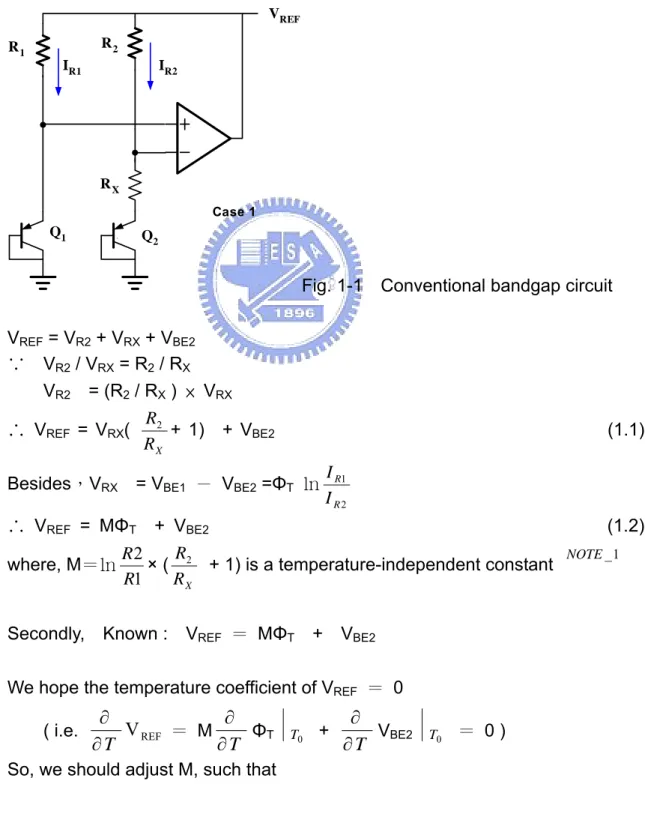
(17) 1.2.2 Conceptual Implementation 1.2.2.1 Conventional Bandgap Circuit Fig.1-1 shows a conventional bandgap circuit. Two components build up the bandgap reference voltage, VREF. One is the voltage across a directly BJTconnected diode (VBE), and the other is ΦT, a term proportional to the absolute temperature (PTAT). VREF R2. R1 IR1. IR2. RX Case 1. Q1. Q2. `. Fig. 1-1. Conventional bandgap circuit. VREF = VR2 + VRX + VBE2 ∵ VR2 / VRX = R2 / RX VR2 = (R2 / RX ) × VRX R2 + 1) + VBE2 RX. ∴ VREF = VRX( Besides,VRX. Secondly,. I R1 I R2. = VBE1 - VBE2 =ΦT ㏑. ∴ VREF = MΦT where, M=㏑. (1.1). + VBE2. (1.2). R R2 × ( 2 + 1) is a temperature-independent constant RX R1. Known :. VREF = MΦT +. VBE2. We hope the temperature coefficient of VREF = 0 ( i.e.. ∂ ∂ V REF = M ΦT ∂T ∂T. T0. +. So, we should adjust M, such that. 3. ∂ VBE2 ∂T. T0. = 0). NOTE _ 1.
(18) M. ∂ ΦT ∂T. Step 1 ∵ΦT =. T0. (1.3). =0. KT q. ∂ 1 1 K KT ΦT = = × = ΦT ∂T q q T T. ∴. Step 2. ∂ V BE2 ∂T. +. T0. ∂ ∂ VBE2 = [ΦT × ㏑( IR2∕IS ) ] ∂T ∂T ∂ ∂ = ( ΦT ) ㏑(IR2∕IS ) + ΦT (㏑IR2-㏑IS ) ∂T ∂T ∂ 1 = ΦT ㏑(IR2∕IS ) - ΦT (㏑IS ) ∂T T. Where. 3. IS = BAE T exp (﹣ VGO =. VG 0. φT. ). NOTE _ 2. E g ( Si ). (1.4). (1.5). (1.6) (1.7). q. B is a temperature-independent constant AE is the base-emitter junction area Eg(Si) is the band gap energy of Silicon. So,. ∂ ∂ V 1 VBE2 = ΦT㏑(IR2∕IS) - ΦT (㏑(BAE) + 3 ㏑T - G 0 ) ∂T ∂T T φT =. V 1 1 V BE2 - Φ T × 3 - G0 T T T. 4. (1.8).
(19) Step 3. Substituting (1.4) and (1.8) into (1.3) gives. ∂ ∂ V REF = M ΦT ∂T ∂T = M. T0. MΦ T0 = 3Φ T0 +. So,. M = 3. VREF. T0. V 1 1 3 Φ T0 + V BE2 - Φ T × - G0 = 0 T0 T0 T0 T0. We derive. Step 4. ∂ VBE2 ∂T. +. +. VG0 - VBE2. ( VG0 - VBE2. T0. (1.9) (1.10). ) ∕Φ T0. (1.11). Substituting M into (1.2) gives = MΦ T0 +. VBE2. = (3Φ T0 + = 3Φ T0 +. VG0 - VBE2). +. VBE2 (1.12). VG0. Finally, The bandgap voltage of silicon VGO =. So that, VREF = 3 × (25.6 mV) +. 1.205 V. 5. E g ( Si ) q. = 1.205 V. = 1.282V. (1.13).
(20) Note_1:. We set. M =㏑. R2 R × ( 2 + 1) which is temperature – independent. R1 RX. In fact, the individual resistances (R1, R2, RX) will vary its value with temperature. But the ratio can keep nearly constant, that is,. R 2 + ΔR 2 R2 ≒ R1 + ΔR1 R1. independent of temperature. Proof:. ΔR 2 =. ∂R 2 ∂R1 ΔT and ΔR1 = ΔT ∂T ∂T. R 2 + ΔR 2 = R1 + ΔR1. ∂R 2 1 ∂R 2 × ΔT R 2(1 + ΔT ) ∂T R 2 ∂ T = ∂R1 1 ∂R1 R1 + ΔT R1(1 + × ΔT ) ∂T R1 ∂T. R2 +. ∵. 1 ∂R 2 1 ∂R1 × ΔT ≅ × ΔT R 2 ∂T R1 ∂T. ∴. R 2 + ΔR 2 R2 ≒ R1 + ΔR1 R1. Similarly,. (1.14). R R 2 + ΔR 2 ≒ 2 RX R X + ΔR X. (1.15). (1.16). when temperature change. 6. (1.17).
(21) Note_2:. q × AE × ni2 × Dn 2 IS = = B '× n i × D n QB. ni. :. QB AE. : the total base doping density per unit area : emitter – base junction area. B'. :. Where. intrinsic minority – carrier concentration. temperature – independent constant. By Einstein equation :. ∴ IS = Set. μn. 2. B '×. =. Dn. ,. Dn. = ΦT ×. μn. K × ni2 × T × μ n q. (1.19). (1.20). μn. μn. = CT. ni2. = DT 3 exp ( −. −n. q × KT. =. B '× ni2 × ( μ nφT ). IS = B ' '× n i × T ×. Known. (1.18). , C is a temperature – independent constant VG 0. φT. ) , D is a temp. – independent constant. Finally, we assume n = 1 and get IS = B ' '× DT 3 exp ( −. VG 0. φT. CT −1. ) ×T ×. = B × AE × T 3 × exp ( −. VG 0. φT. ). (1.21). 7.
(22) 1.2.2.2 Recently Proposed Bandgap Circuit According to the previous analysis, If the power supply voltage is lower than 1.28V, the conventional bandgap reference circuit cannot be used. In order to meet the demand that power supply voltage is lower than 1.3V, one solution was proposed by using current-mode structures and low operating voltage of OP-Amplifiers to achieve the low voltage (VDD ≤ 1.0V) bandgap reference circuit as shown in Fig. 1-2 and described below [8]. VDD M3. M2. M1. I2. VREF. I3. R3. Vd1. IR2A. R1. Vd2. IR1. R2B. R2A Q1 m=8. Fig. 1-2. Q2. Typical current-mode bandgap circuit. Q I 3 = I 2 = I R 2 A + I R1 and R 2 A = R2 B then, we can derive I R 2 A = I R 2 B ∴VREF = I 3 R3 = ( I R 2 A + I R1 ) R3 = ( I R 2 B + I R1 ) R3 =(. VEB2 VEB2 − VEB1 + ) R3 R2 B R1. = VEB 2. R3 R3 + (ln 8 )φT R 2B R 1 8. IR2B.
(23) Fig. 1-2 shows a typical current-mode BGR circuit topology. First, we set Vd1=Vd2 by utilizing the OPA negative feedback characteristic. Second, according to the BJT device physics, the circuit will create two currents, which are IR1 and IR2A. The current IR1 will increase as the temperature increase, which is called the positive temperature coefficient. And the current IR2A will decrease as the temperature increase, which is called the negative temperature coefficient. Theoretically, these two currents (IR1 and IR2A) will compensate to each other. So we can get a new stable current which is independent of temperature by adding these two currents (IR1 and IR2A). Finally, making the new stable current (I3) pass through a resistor can produce the so-called reference voltage. According to the theory, it is possible to achieve 0.7V reference with 1.0V power supply voltage and a well-controlled temperature behavior. However, the OP-Amplifier is the most critical block. The supply voltage used must ensure correct operation of the operational amplifier and, indeed, it is the true limit of the circuit. So, how to design a good OP-Amplifier is an important issue and the detail will be presented in chapter 2 and chapter 4.. 9.
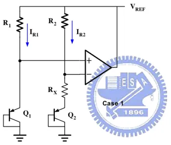
(24) 1.3. Review on CMOS Bandgap Reference Circuits (II). There are several kinds of bandgap reference circuits. In this section, we will introduce and discuss the most representative circuits from the conventional one to the recently proposed ones. We can roughly classify the BGR circuits into two categories, the sum of voltage ( Class-A ) ; the sum of currents ( Class-B ). 1.3.1. The Class-A of Bandgap Circuit (The Sum of Voltage). Case1:. [5] VREF R2. R1 IR1. IR2. RX Case 1. Q1. `. Q2. Fig. 1-3 The case1 bandgap circuit with VDD > 1.0V and VREF > 1.0V. VREF = I R1 R1 + VEB1 = I R 2 R2 + VEB1 =. VEB1 − VEB 2 R2 + VEB1 RX. =. R2 R ln( 2 )φT + VEB1 RX R1. 10.
(25) Case2 :. VREF = ( I R1 + I R 2 ) R4 + VBE1. [6] Vcc. = I R2 ( R2. R1. I R2. IR1. V REF. I R1 + 1) R4 + VBE1 I R2. =(. VBE1 − VBE 2 R2 )( + 1) R4 + VBE1 R3 R1. =(. R2 R R + 1) 4 ln( 2 )φT + VBE1 R1 R3 R1. Q2. Q1. R3 Case 2. R4. Fig. 1-4 The case2 band-gap circuit with VDD > 1.0V and VREF > 1.0V. Case3 :. VREF = I R 2 R2 + VEB 2. [7]. VDD. VREF R2 R1. IR1 Q1 m=8. =. VBE2 − VBE1 R2 + VEB 2 R1. =. R2 I (ln R 2 )φT + VEB 2 R1 I R2 / 8. =. R2 (ln 8)φT + VEB 2 R1. IR2 Q2 Case 3. Fig. 1-5 The case3 Band-gap circuit with VDD > 1.0V and VREF > 1.0V. 11.
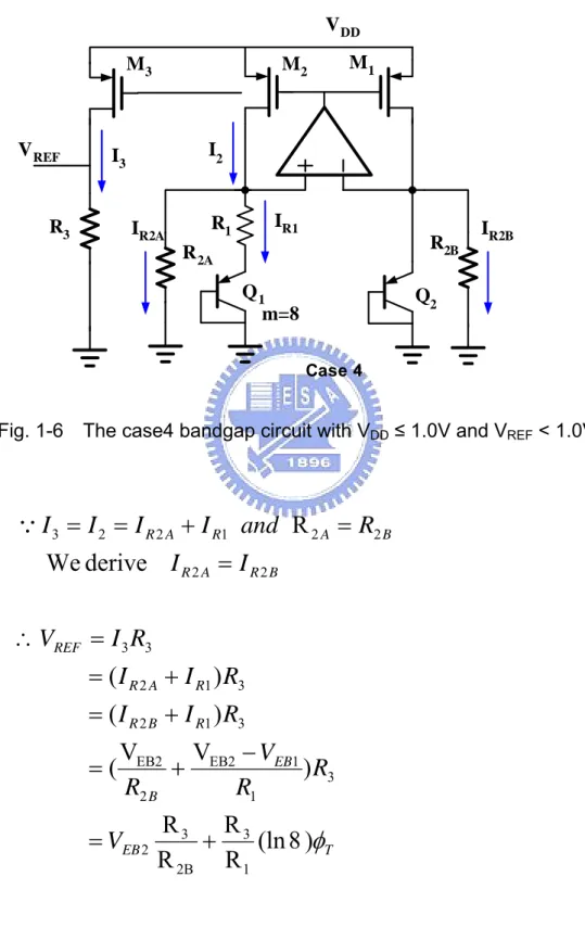
(26) 1.3.2. The Class-B of Bandgap Circuit (The Sum of Current). Case4 :. [8]. V DD M3. V REF. M2. I2. I3. R3. M1. IR2A. IR1. R1. R2B. R 2A Q1 m=8. IR2B. Q2. Case 4. Fig. 1-6 The case4 bandgap circuit with VDD ≤ 1.0V and VREF < 1.0V. Q I 3 = I 2 = I R 2 A + I R1 and R 2 A = R2 B. We derive I R 2 A = I R 2 B ∴VREF = I 3 R3 = ( I R 2 A + I R1 ) R3 = ( I R 2 B + I R1 ) R3 =(. VEB2 VEB2 − VEB1 ) R3 + R2 B R1. = VEB 2. R3 R3 + (ln 8 )φT R 2B R 1. 12.
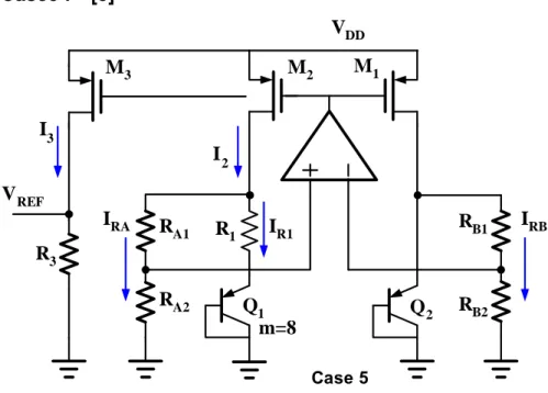
(27) Case5 :. [3]. VDD M3. M1. M2. I3 I2 V REF IRA. RA1. R1. RB1. IR1. IRB. R3 RA2. Q1 m=8. Q2. RB2. Case 5. Fig. 1-7 The case5 bandgap circuit with VDD ≤ 1.0V and VREF < 1.0V. Q I 3 = I 2 = I RA + I R1 and R A1 = RB1 , R A 2 = RB 2. We derive I RA = I RB ∴VREF = I 3 R3 = ( I RA + I R1 ) R3 = ( I RB + I R1 ) R3 =(. VEB2 V − VEB1 ) R3 + EB2 RB1 + RB 2 R1. = VEB 2 Table-1. R3 R + 3 (ln 8 )φT R B1 + R B2 R 1. Classification of bandgap reference circuits Class A (the sum of voltages). Class B (the sum of currents). VDD > 1.0V case-1, case-2, case-3. Type C and Type D of this thesis ( by TSMC 0.35μm ). VDD ≤ 1.0V. case4, case5, and Type A & Type B of this thesis ( by TSMC 0.18μm ). 13.
(28) 1.4 Organization of This Thesis This thesis is divided into six chapters. In Chapter 1, the background and motivation are presented and the representative bandgap circuits are classified and introduced. Furthermore, we construct a complete classification as shown in Table-1. In Chapter 2, Type A and Type B bandgap circuits based on the class B topology implemented by TSMC 0.18μm CMOS process was proposed. The design consideration is discussed in section 2.1. Then the design concepts including VREF and PSRR are presented in sections 2.2 and 2.3. The circuit realization is described in section 2.4. In chapter 3, the circuits layout based on TSMC 0.18μm CMOS process is presented. The chip testing result and comparison with simulation are shown in the following subsections. In Chapter 4, we improve the circuits topology proposed on chapter 2, to create two new types of bandgap circuits, which are named as Type C and Type D. The new topology ensures that the circuits can meet all process corners. The organization of chapter 4 is the same as chapter 2. The design consideration is discussed in section 4.1. Then the design concept is presented in section 4.2. The circuit realization is detailed in section 4.3. In chapter 5, the circuits’ layout based on TSMC 0.35μm CMOS process is presented. The chip testing result and comparison with simulation are shown in the following subsections. In chap 6, conclusion and future work are given.. 14.
(29) Chapter 2 DESIGN OF LOW VOLTAGE HIGH PSRR BANDGAP REFERENCE CIRCUIT WITH TSMC 0.18μm CMOS PROCESS 2.1. Design Motivation. Until now, most OPAs in the bandgap circuits use pMOS as the differential pair because the conventional bandgap circuit topology limit the common mode voltage of OPA. For example, if we use nMOS as the OPA’s input stage then the input common-mode voltage of the OP-Amplifier must meet the following condition, as shown in Fig. 2-1 [3]: VCOMM = Vthn + 2VDS(sat) < VEB(ON)≒ 650mV The above condition implies that Vthn < 550mV is required (assuming VDS(sat) = 50mV). This requirement can be satisfied in many technologies, but it is only for TT (Typical – Typical) process. However, considering the other process corner (e.g. SS and SF), the above requirement cannot be easily satisfied. Take TSMC 0.18μm 1P6M CMOS technology as an example: Vthn = 440mV at Typical case, but Vthn = 540mV at slow corner (S).. VDD M2. M1. M3. VREF VB. R3 R1 R2B. R2A Q1 m=8. Fig. 2-1. Q2. Bandgap circuit that uses nMOS as input stage. 15.
(30) Because of the circuit structure limitation as mentioned above, most bandgap circuits were implemented by using pMOS as the OPA’s differential pair. But there are two disadvantages when using pMOS as the differential pair. One is the smaller voltage gain due to the smaller gm for pMOS. The other disadvantage is that the OPA’s offset voltage will be multiplied by R3 R A 2 when using pMOS as the differential pair. By contrast, the OPA’s (1 + ) R1 R A1. offset voltage will only be multiplied by ( R 3 ) if we use nMOS as the differential R1. pairs. NOTE_3. .. NOTE_3. Discuss the impact of the OPA’s offset voltage on different bandgap circuit topology where Fig. 2-2 shows the pMOS as the OPA’s input differential pair while Fig. 2-3 shows the nMOS as the OPA’s input differential pair.. (A) Bandgap circuit that use pMOS as differential pair VDD M3. M1. M2. I3 I2 IRA. RA1. R1. IR1. R3 RA2. Fig. 2-2. VB. VA. VREF. RB1. Vos. Q1 m=8. Q2. IRB. RB2. Bandgap circuit that uses pMOS as differential pair. 16.
(31) (1) V A (. R A2 R B2 ) − V os = V B ( ) R A1 + R A 2 R B1 + R B 2. Q V A = I R1 R 1 + V EB 1 , V B = V EB 2 , ( ∴ ( I R1 R 1 + V EB 1 )(. R A2 R B2 ) − V os = V EB 2 ( ) R A1 + R A 2 R B1 + R B 2. We derive ( I R1 R 1 + V EB 1 ) − (. R A1 + R A 2 )V os = V EB 2 R A2. I R1 R 1 = V EB 2 − V EB 1 + (. So. I R1 =. Finally. ( 2 ) I 2 = I R 1 + I RA. = I R 1 + V EB 2 (. R A2 R B2 )=( ) R A1 + R A 2 R B1 + R B 2. R A1 + R A 2 )V os R A2. 1 1 R A1 + R A 2 (φ T ln m ) + ( )V os R1 R1 R A2. (2.1). and I RA = I RB. R B1. 1 ) = I R3 + RB2. (2.2). ( 3 ) V REF = I 3 R 3 = I 2 R 3 = I R 1 R 3 + V EB 2 (. =. R3 R R3 R (φ T ln m ) + 3 (1 + A 2 )V os + V EB 2 ( ) R1 R1 R A1 R B1 + R B 2. (4) Substituting V REF =. R3 ) R B1 + R B 2 (2.3). m=8. R3 R R3 R A2 ( φ T ln 8 ) + 3 (1 + )V os + V EB 2 ( ) R1 R1 R A1 R B1 + R B 2. (2.4). (5) Unfortunately, Vos is not independent of temperature. Even worse, it will be multiplied by R 3 (1 + R A 2 ) , when using pMOS as differential pair. R1. R A1. 17.
(32) (B) Bandgap circuit that use nMOS as differential pair V DD M3. V R EF. I2. I3. R3. I R 2A. M1. M2. VA. V os. IR 1. R1. R 2B. R 2A Q1 m =8. Fig. 2-3. VB I R 2B. Q2. Bandgap circuit that uses nMOS as differential pair. (1) V A − V os = V B Q V A = I R 1 R 1 + V EB 1 , V B = V EB 2 ∴ ( I R 1 R 1 + V EB 1 ) − V os = V EB 2 We derive I R 1 R 1 = V EB 2 − V EB 1 + V os So I R 1 =. 1 1 (φ T ln m ) + V os R1 R1. (2.5). ( 2 ) I 2 = I R 1 + I R 2 B ( I 2 = I R 1 + I R 2 A and I R2A = I R 2 B ) = I R 1 + V EB 2 (. 1 ) R2 B. (2.6). ( 3) V REF = I 3 R 3 = I R 1 R 3 + V EB 2 ( =. R3 ) R2 B. R3 R R (φ T ln m ) + 3 V os + V EB 2 ( 3 ) R1 R1 R2 B. 18. (2.7).
(33) (4) Substituting. V REF =. m=8. R3 R R (φT ln 8) + 3 Vos + V EB 2 ( 3 ) R1 R1 R2 B. (2.8). (5) Unfortunately, Vos is not independent of temperature. But, it will only be amplified by (. R3 ), when using nMOS as differential pair. R1. So, in this chapter, we modify the bandgap core circuit to break through the limitation on OPA when using nMOS as the differential pair. Hope to create a new kind of bandgap circuit in which the OPA’s differential pair is composed of nMOS. In this way, the new topology of bandgap circuit will occupy less layout area but provide better performance than the existing topology using pMOS as the OPA’s differential pair.. 19.
(34) 2.2. Bandgap Reference Circuit Design Concepts (I). VDD M2. M1. M3. VREF VB. RY. RX. R3. I. R1 R2A. R2B Q1 m=8. Q2. Fig. 2-4 Bandgap circuit inserting RX, RY to upgrade common-mode voltage As shown in Fig. 2-4, after inserting another resistor pair, RX and RY, (as marked by red circle), the “the input common-mode voltage of the OP-Amplifier” is no longer restricted to the VEB(ON), That is Vthn + 2VDS < VEB(ON) + I × RY ≒ 750 mV So the bandgap core circuit will provide a common-mod voltage that is large enough to drive OPA’s nMOS differential pair and keep it working in the saturation region. Finally the OPA will provide large voltage gain to drive the bandgap core circuit, It is another feature in this thesis that the output reference voltage can reach 760 ~ 800 mV, which is higher than the others proposed by existing papers, as shown in Table-2.. 20.
(35) Table-2. Comparison of low-voltage bandgap reference test chip. Technology Threshold Voltage. This work. This work. This work. This work. Type A. Type B. Type C. Type D. 0.18-μm. 0.18-μm. 0.35-μm. 0.35-μm. CMOS. CMOS. CMOS. CMOS. Vthp = -0.44V Vthp = -0.44V Vthp = -0.74V Vthp = -0.74V Vthn = +0.44V Vthn =+0.44V Vthn =+0.54V Vthn = +0.54V. Min Vdd. 1.10V. 1.10V. 1.30V. 1.10V. 1.1 ~ 3.0V. 1.1 ~ 3.0V. 1.3 ~ 4.5V. 1.1 ~ 4.5V. Max. Supply currets. 38.1μA. 34.4μA. 54μA. 41μA. Vref (參考電壓). 772mV. 737mV. 766mV. 829mV. Power Supply Range. (工作電壓). TCF(eff). 140 ppm /℃. 149 ppm /℃ 90.2 ppm /℃. 34.1 ppm /℃. (-40 ~ 140℃). (-40 ~ 140℃) (-20 ~ 100℃). (-40~120℃). PSRR for 1KHz. - 56dB. - 51dB. -18dB. -25dB. PSRR for 10KHz. - 29dB. - 33dB. -2.7dB. -10dB. PSRR for 100KHz. -15.2dB. Size. 0.192 mm. -26dB 2. -0.1dB 2. 0.145 mm. -0.42dB 2. 0.294 mm. Ka Nang Leung J. Doyle et al. Neuteboom. 0.238 mm2. Malcovati et al.. [3]. [2]. et.al [19]. [1]. AMS 0.6-μm. 0.5-μm. 0.8-μm. 0.8-μm. CMOS. CMOS. CMOS. BiCMOS. Threshold. Vthp = -0.9V. N/A. Vthp = -0.7V. Vthp = -0.7V. Voltage. Vthn = +0.9V. Vthn = +0.5V. Vthn = +0.7V. Min Vdd. 0.98V. 0.95V. 0.90V. 0.95V. 0.98 ~ 1.5V. 0.95 ~ 6.0V. N/A. 0.95 ~ 2.0V. 18uA. 10.0uA. N/A. < 92.0uA. 603mV. 626mV. 670mV. 536mV. 15 ppm /℃. 17 ppm /℃. N/A. 19 ppm /℃. (0~100℃). (-40 ~ 125℃). PSRR for 1KHz. N/A. N/A. N/A. N/A. PSRR for 10KHz. - 44dB. N/A. N/A. N/A. PSRR for 10MHz. - 17dB. N/A. N/A. N/A. 0.24 mm2. 1.09 mm2. N/A. N/A. Technology. Power Supply Range. (工作電壓) Max. Supply currets Vref (參考電壓) TCF(eff). Size. 21. (0~100℃).
(36) From Table-2, the output reference voltage proposed in this thesis is 760 ~ 800mV, while the others is about 600 ~ 670mV. The reason is that HSPICE simulation suggests the best PSRR corresponding to Vref = Vd1 = Vd2 as shown in Fig. 2-5. Taking Fig. 2-5 with TSMC 0.18μm CMOS process as an example, the best PSRR performance occur at Vref = 675mV, marked by the red circle in the Table-3.. Table-3. Simulation result of PSRR at Vd1 = Vd2 = 670mV based on TSMC 0.18μm CMOS process. R3. 70k. 80k. 90k. 100k. 110k. 120k. 130k. Vref. 473mV 540mV 607mV 675mV 742mV 808mV 874mV. PSRR(DC). -60dB. -61dB. -64dB. -84dB. -56dB. -45.8dB -36.2dB. PSRR(10kHz) -60dB. -61dB. -64dB. -84dB. -56dB. -45.8dB -36.2dB. Note:PSRR = 20 log ( 20/20 M=12. 20/20 M=12. 20/20 M=12. M1. M3. M2 Vdd. 1.2Vdc. 3. Vd1. 0. 11. 670 mV. -. V-. Vd2. 2. 670 mV. Vref. OUT. 1. 675 mV. V+ +. 4. R1 R3. 100k. ΔVref ) ΔVdd. 26k R2A. 185k. R2B Q1. 185k. Q2. m=24 0. Fig. 2-5. Conventional BGR circuit topology. However, Vref = 675mV cannot meet the industrial requirement. For IC design industry, the Vref should be 750mV ~ 800mV. But, if we increase the reference voltage to 750mV by only adjusting the resistor R3 value, the PSRR performance will degrade rapidly, as shown in Table-3.. 22.
(37) Now, by inserting resistor pairs, RX and RY, we get another advantage: increase Vd1 and Vd2 voltage to 760mV. In this manner, the PSRR is optimal corresponding to Vref = Vd1 = Vd2 = 760mV, as shown in Fig. 2-6 and Table-4. 20/20, M=12. 20/20, M=12. 20/20, M=12. M1. M2. 760 mV Vd1. 0. 11. 760 mV. -. +. V-. Vd2. 2. Vref. V+. 3. 767 mV. LM324. OUT. 4. Vdd 1.2Vdc. 1. M3. Rx R3 100k. Ry. 30k R2A. R1. R2B 163k. 27k Q1. 163k. 30k. Q2. m=24 0. Fig. 2-6. Modified BGR circuit topology proposed in this thesis. Table-4 Simulation result of PSRR at Vd1 = Vd2 = 760mV based on TSMC 0.18μm CMOS process, known Vd1 = Vd2 = 760mV R3. 80k. 90k. 100k. 110k. 120k. 130k. Vref. 540mV. 607mV. 767mV. 742mV. 808mV. 874mV. PSRR(DC). -61dB. -64dB. -69dB. -56dB. -45.8dB. -36.2dB. PSRR(10kHz). -61dB. -64dB. -69dB. -56dB. -45.8dB. -36.2dB. In this thesis,we provide Vref ≒ 735 ~ 800 mV, which is higher than the output reference voltages provided by other papers, i.e. around 600mV, and much more meet the industrial requirement. Besides, we can keep the PSRR at the optimal state and maintain a well-controlled temperature compensation performance as shown in the Table-2.. 23.
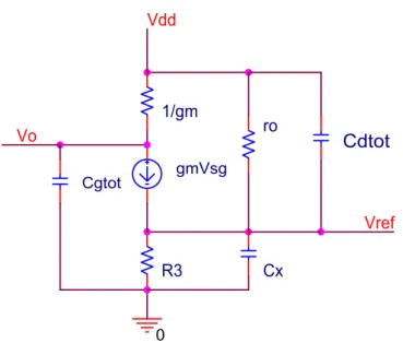
(38) 2.3. Bandgap Reference Circuit Design Concepts (II). The preceding description is based on the simulation result. In order to get more conviction, we try to formulate the simulation result by using MOS small signal model and equivalent circuit to analyze.. (1) For simplification, we only analyze the mechanism of the PSRR of M3, as marked by the circle shown in the Fig. 2-6. 20/20, M=12. 20/20, M=12. 20/20, M=12. M1. M2. OUT. V-. 3. Vd1. 0. 11. 760 mV. -. 760 mV. Vref. V+. Vd2. 2. 767 mV. LM324. +. 4. Vdd 1.2Vdc. 1. M3. Rx R3 100k. Ry. 30k R1. R2A 163k. 30k. 27k. R2B 163k. Q1. Q2. m=24 0. Fig. 2-6. Modified BGR circuit topology proposed in this thesis. (2) Set up the equivalent circuit of pMOS M3 for analyzing the mechanism of the PSRR as shown in Fig. 2-7. Vdd. 1Vac. Vdd. 3Vdc 0. 1.00093Vac 1.5Vdc. 20/20 M=12. Vo M3. Vref. Vg. R3 0. Fig. 2-7 Analysis of the single pMOS device (M3) for PSRR study. 24.
(39) The small signal model as shown in Fig. 2-8: Vdd. 1/gm Vo. ro. Cdtot. gmVsg. Cgtot. Vref R3. Cx. 0. Fig. 2-8 Small signal model analysis of pMOS device (M3) for PSRR study. The PSRR formula can be derived as follow: s + WZ Vref Vo 1 =gm R3 ( 1 − )( ) + K( ) s + WP Vdd Vdd 1 + sR3C dtot. =gm R3 ( 1 −. C dtot s + WZ Vo 1 )( ) + ( ) C dtot + C X s + WP Vdd 1 + sR3C dtot. Where. Wz = (1 / roCdtot), Wp = [ 1 / (ro|| R3 ) (Cdtot+CX ) ], Cdtot >> CX. And. CX is negligible. From Table-4, we know that PSRR will be at the optimal state when Vd1 = Vd2 = 760mV. We now analyze the device parameter based on different bandgap reference voltage (Vref) as shown in Table-5.. 25.
(40) Table-5 Simulation result of the different bandgap reference voltage based on TSMC 0.18μm CMOS process R3. 70k. 80k. 100k. 110k. 130k. Vref. 538mV. 540mV. 767mV. 742mV. 874mV. Id. 7.68uA. 6.75uA. 7.67uA. 6.74uA. 6.72uA. gm. 92.9u. 85.6u. 92.7u. 85.5u. 85.2u. Vds. 661mV. 659mV. 432m. 458mV. 325mV. gds. 61.6n. 55.48n. 103n. 81.0n. 187n. ro. 16.2M. 18.02M. 9.70M. 12.3M. 5.34M. ΔVref / ΔVdd. -2.69m. -873.5u. 334u. 1.60m. 15.4m. Vo / Vdd. 1.0010799 1.0007751 1.0010799 1.0007751 1.0007751. PSRR (DC). -51.3dB. -61dB. -69.5dB. -55.9dB. -36.2dB. Cdtot. 295f. 295.8f. 309f. 308f. 317f. Cgtot. 27.3p. 26.9p. 27.3p. 26.9p. 26.9p. Cstot. 31.8p. 31.08p. 31.8p. 31.08p. 31.08p. Cbtot. 11.1p. 11.12p. 11.1p. 11.12p. 11.12p. Cgs. 23.5p. 22.95p. 23.5p. 22.95p. 22.95p. Cgd. 78.6f. 78.60f. 78.6f. 78.60f. 78.60f. Wp(rad/sec). -48.5M. -42.44M. -32.6M. -29.7M. -24.7M. Wz(rad/sec). -2.69M. -1.37M. -6.35M. -3.00M. -7.88M. For hand calculation: R3 = 70k R3 Vref Vo 70k = gm R3 ( 1 − )+( ) =92.9u * 70k(1-1.0010799) + ro + R3 Vdd Vdd 16.2M + 70 K = - 0.0070225 + 0.0043023 = - 0.00272 = - 2.72m. PSRR for DC = |. Vref | dB = 20 log (2.72m) = - 51.3dB ( S:- 51.4dB ) Vdd. And the frequency of dominant pole Wp = [ 1 / (ro|| Rd )( Cdtot + CX ) ] = 1 / ( 70k × 295f ) = - 48.42 M rad /sec Good match with the simulation, Wp = - 48.5M rad/ sec. 26.
(41) (1) R3 = 100k R3 Vref Vo = gm R3 ( 1 − )+( ) ro + R3 Vdd Vdd. =. 92.7u * 100k(1-1.0010799) +. 100k 9.7 M + 100 K. = - 0.0100106 + 0.010204 = 0.0001934 = 193.4u. PSRR for DC = |. Vref | dB =20 log (193.4u) = - 74.26dB ( S:- 69.5dB ) Vdd. Good match with the simulation , PSRR = - 69.5 dB. (3) R3 = 130k. Vref 130k = 85.2u × 130k (1-1.0007751) + Vdd 5.34M + 130 K = - 0.008585 + 0.0237659 = 0.0151809 = 15.18m. PSRR for DC = |. Vref | dB =20 log (15.18m) = - 36.37dB ( S:- 36.2dB) Vdd. Good match with the simulation , PSRR = - 36.2 dB. Conclusion: From the derived formulas, we see that PSRR is composed of two terms. The first term is always a negative value, while the second term is always a positive value. When Vd1 = Vd2, the first term and the second term cancel each other. That behavior makes the PSRR approach to minimum value, that is, best performance. So, the theoretical analysis of MOS small signal equivalent circuit can prove the simulation result.. 27.
(42) 2.4. Circuit Implementation. In chapter two, there are two types of BGR circuits. The bandgap core circuits are the same, as shown previously, but the OP-Amplifiers are different. The first circuit (a conventional one) named as Type A uses pMOS as the input stage, as shown in Fig. 2-9, while the second circuit celled as Type B uses nMOS as the input stage, as shown in Fig. 2-10. Here, one important thing we want to mention is that in conventional BGR circuits, the emitter area ratio of BJT Q1 and Q2 is usually 8:1. So, the △VBE is about 50mV in the conventional BGR circuits. Note:△VBE = ΦT * ln(m) = 26mV * ln (8) = 54.06mV But, According to reference paper [2]: “ A large△VBE can reduces the effect of amplifier input offset ”。 And this conclusion can be verified by the formulas (2.3) or (2.7). So, in this thesis, we put the emitter area ratio of BJT Q1 and Q2 to 24:1. In this way, the △VBE is increased to around 80mV。 Finally, the simulated features of the two types of OP-Amplifier are summarized in Table-6.. Table-6 Operational Amplifier features of Type A and Type B Type A. Type B. pMOS as the input stage. nMOS as the input stage. 65 dB. 70 dB. 6.5 MHz. 10.5 MHz. Phase Margin. 51.8°. 80.1°. Supply Voltage. 1.10 V. 1.10 V. DC Loop gain Gain-Bandwidth product. 28.
(43) Here below is the complete circuit topology of Type A and Type B. bandgap core 20/20 m=12. 20/20 m=12. M3. start-Up. OP-Amplifier. 20/20 m=12. M1. 20/10 m=2 Rs1 1000k. M2. 20/10 m=3. 20/10 m=2 MA04. MA01. 20/20 m=12. Vdd 1.11Vdc. MA05 MA14. MS2. Rs2 300k. Vd1 Rx. R2A1. diff 105k R3. R2B1 diff 105k. R1. Vn. Vo. D1 D2. Ry. po14k po14k. MA15. 0. 20/10 m=6. Vref. 20/20 m=12. 10/5 20/10. 10/5. MA08. MA09. MS5. Vp. diff 80k. po15k. R2A2 diff 70k. MA12. m=24. Q1. Q2. R2B2. MS1. diff 70k. MA13. 20/20. 0. MA02. MA03. 10/20. Fig. 2-9. 10/20. MA10. MA11. 5/10. 5/10. 20/20 m=2. 20/20 m=2. The complete bandgap circuit topology of Type A (bandgap core + start-Up + OP-Amplifier with pMOS input stage). Bandgap core. 20/20 m=12. 20/20 m=12. M3. start-Up. OP-Amplifier. 20/20 m=12. M1. 20/10 m=7 MA01. Rs1 diff 1000k. M2. 20/20 m=7. 20/20 m=7. MA10 MA11. Vdd 1.11Vdc. Vo. 20/10 m=6. Rs2 diff 300k. MS2. 0. D2 D1. Vnon Vref. Rx po 14k R3. R1. diff 80k. R2A diff 175k. 20/10. Vinv. MA08. Ry po 14k. 20/10 MA09. po 15k. Q2. Q1 m=24. R2B diff 175k. MS5 20/10 m=2. MS1 20/20. MA02. 0. Fig. 2-10. 20/10. MA03. 20/10. The complete bandgap circuit topology of Type B (bandgap core + start-Up + OP-Amplifier with nMOS input stage). 29.
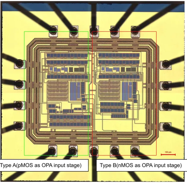
(44) Chapter 3 CHIP LAYOUT DESCRIPTION AND EXPERIMENTAL RESULTS WITH TSMC 0.18μm CMOS PROCESS 3.1 Chip Layout Descriptions The test chip is designed and fabricated by TSMC 0.18μm single-poly-sixmetal (1P6M ) CMOS technology. Fig. 3-1 shows the overall die photo of the Type A and Type B, which include the bandgap core circuit and OP-Amplifier. The chip area is 0.192 mm2 for Type A and 0.145 mm2 for Type B. The transistors used are totally 21 for Type A, 15 for Type B. The bandgap core circuit in Fig. 3-1 consists of the startup circuits, bipolar transistors, bias resistors, and the MOS transistors that provide the current through the bias resistors and the BJT group (Q1 & Q2), respectively. Since the mismatching of the MOS transistors in the differential pair will make the current different, the same size MOS transistors are placed as close as possible to minimize this kind of mismatching. The most important devices in the bandgap circuit are the bipolar transistors with large thermal coefficient. The parasitic vertical PNP BJTs are used in this test chip. The layout should be arranged carefully to ensure matching and accurate ratio of these BJTs. Thus, we choose the ratio of the emitter area of Q1 and that of Q2 to be 24, and arrange the 24 Q1s to circulate the single Q2. The reason why we choose the ratio to be 24 has been explained in the section 2.4. The total emitter area of Q1 is 2400um2 and that of Q2 is 100 um2 in this layout. This arrangement not only reduces the mismatching of these bipolar transistors, but also makes the temperature coefficient of these bipolar transistors as close as possible . The accuracy of the resistance value on the chip is the most difficult job to realize in the process. Hence, the output reference voltage is designed to be dependent on the ratio instead of absolute value. Besides, a unit dimension of the resistors is defined, and all the resistors are series-connected by the unit resistors in order to reduce the mismatching of the resistors arising process non-uniformity.. 30.
(45) Type A(pMOS as OPA input stage). Fig. 3-1. Type B(nMOS as OPA input stage). The overall die photo of the Type A and Type B. Note:In this test chip, a set of I/O PAD library developed by ITRI (Industrial Technology Research Institute) was chosen to use. The detailed library name is “STC Pure 1.8V Linear I/O Library in 0.18μm CMOS process, version 1.0”. 31.
(46) 3.2 Measurement Setup (1) The set up required to measure “Vref (Reference Voltage) vs. Vdd ” are power supply and voltage meter. (2) The set up required to measure “Transient Response curve” are power supply, function generator, and Oscilloscope。Fig. 3-2 shows an example of measured transient response for Type B (nMOS as OPA’s input stage) where the output voltage of the function generator is set up from 1.3V to 2.3V。. Fig. 3-2. Typical transient response curve. (3) The PSRR for high freq. (from 50KHz to 10MHz) can be calculated by the output waveform as shown in Fig. 3-3, which was produced by using the power supply、Function generator and Oscilloscope. Fig. 3-3 shows the PSRR of Vref at freq. = 50KHz, where the input supply voltage is a Sin Wave (amplitude = 131mV). And the output reference voltage is also a Sin Wave (amplitude= 121mV).. Fig. 3-3. PSRR of n-Vref at freq. = 50KHz at AC mode. 32.
(47) Calculation: Take Fig. 3-3 as an example, in which frequency = 50KHz; The variation of input power supply voltage is 131mV and the resulted variation of output reference voltage is 121mV. Based on the definition of PSRR we can get. PSRR = 20 log(. 121mV ΔVref ) = 20 log( ) = -0.68 dB at freq. = 50KHz ΔVdd 131mV. (4) As for the measurement set up for PSRR at low frequency (from 100Hz to 50kHz), a network analyzer, power supply and a high gain OP-Amplifier are used. The measurement setup is shown in Fig. 3-4. where PSRR = S21 =. V port _ B V port _ R. 1MΩ Input Adapter Network Analyzer. Port B Port R. RF out. 2. -. V-. 11. bandgap circuit. +. Vdd. Vref. 4. Power Supply. 1. V+. OUT 3. 1.2Vdc 0. Fig. 3-4. The measurement setup for low frequency PSRR test. (5) The measurement of “Temperature Compensation Curve ” is done by the Precision Temperature Forcing System (T-2800). The test chip was put into the chamber, and the temperature was set from -40℃ to 150℃, to measure the output Reference. The temperature was increased by each step of 5℃, to collect the temperature compensation curve and calculate the corresponding temperature coefficient, TCF(eff).. 33.
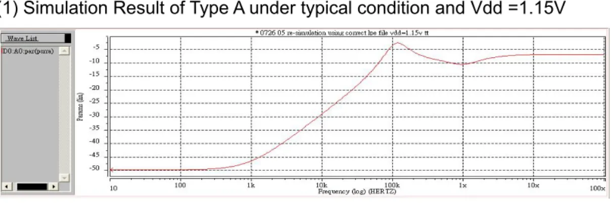
(48) 3.3 Experimental Results 3.3.1 Experimental Results of Type A (pMOS as OPA input stage ) PART (I) Vref (Reference Voltage) vs. Vdd (1) Measured Result of Type A. p-Vref (mV). p-Vref vs. Vdd. 900 800 700. IC No.1 IC No.2. 600. IC No.3 IC No.4 IC No.5. 500 2 .8. 2.6. 2.4. 2 .2. 2. 1 .8. 1.6. 1.4. 1 .2. 1. 0 .8. 0.6. 400 Vdd (V) Fig. 3-5. Measured p-Vref vs. Vdd of Type A. p-Vref (mV). Average of p-Vref. 850.0 800.0 750.0 700.0 650.0 600.0 550.0 500.0 450.0 400.0. p-Vref_mean. 0. 0.5. 1. 1.5. 2. Vdd (V). Fig. 3-6. Average of measured p-Vref vs. Vdd of Type A. Note : mean value = 772.1 mV ; STD value = 42.6 mV. 34. 2.5. 3.
(49) PART (II) Temperature Compensation Curve (1) Simulation Result of Type A at TT. Fig. 3-7. Simulated TC curve of Type A under typical condition axis X : temperature (℃) ; axis Y : p-Vref (mV). (2) Measured Result of Type A TC curve of p-Vref_No.8 at Vdd = 1.2v 760.0 p-Vref (mV). 755.0 750.0 745.0 740.0 735.0 730.0 -50. 0. 50. 100. 150. Temperature (C). Fig. 3-8 TCF(eff) =. Measured TC curve of Type A 1 745 mv. ( 756 − 737 mV )= 141 ppm/℃ 140 − ( −40 ). Fig. 3-8 shows that a dramatic deviation of measured result from the simulation. Why does this IC chip fail to show the correct function of temperature compensation? The process variation associated with diffusion resistor and poly resistor is the root cause. We will have a detailed explanation in section 3.3.2 PART (II).. 35.
(50) PART (III) Transient Response: (1) Simulation Result of Type A at TT. Fig. 3-9. Simulated transient response of Type A under typical condition upper axis X : time (sec) ; axis Y : Vdd (V) lower axis X : time (sec) ; axis Y : p-Vref (mV). (2) Measured Result of Type A. Fig. 3-10. Measured transient response of Type A at AC mode upper axis X : time (sec) ; axis Y : Vdd (V) lower axis X : time (sec) ; axis Y : p-Vref (mV). 36.
(51) PART (IV) PSRR (Power Supply Rejection Ratio) (1) Simulation Result of Type A under typical condition and Vdd =1.15V. Fig. 3-11 Simulated PSRR of Type A under typical condition axis X : frequency (Hz) ; axis Y : PSRR of p-Vref (dB). (2) Measured Result of Type A by using network analyzer and oscilloscope Because of the wide rage of frequencies, we use different measurement set up to collect the PSRR data. 1. For low frequency (from 100 to 100kHz):using network analyzer to collect the data. 2. For high frequency (from100kHz to 5MHz):using oscillator-scope to collect the data. Next, put the measurement and simulation together for comparison, as shown in Fig. 3-12. P S R R ( p M O S d iff- p a ir ) a t V d d = 1 .1 5 v. 20 10. M e a s u re m e n t S im u la tio n. PSRR (dB). 0 S im .. -1 0 -2 0. M ea.. -3 0 -4 0 -5 0 -6 0 -7 0 100. 1k. 10k. 100k. 1M. 10M. F re q . (H z ). Fig. 3-12 Comparison of the measurement and simulation of PSRR of Type A under Vdd = 1.15V 37.
(52) Table-7. Summary table of PSRR for Type A at Vdd = 1.15V. PSRR at 1.15V. DC dB. 10K dB. 50K dB 114K dB 500K dB. 1M dB. simulation. -49.6. -29. -13.2. -2.7. -9.2. -10.5. measurement. -55.9. -28.9. -20.6. -15.2. -6.4. -5.67. Spec.. <-60. <-30. N/A. N/A. N/A. N/A. And Fig. 3-13 shows the PSRR performance of Type A under various Vdd, 1.0V, 1.1V, 1.2V, 2.5V. PSRR (dB). P S R R ( p M O S d iff- p a ir ) fo r v a r io u s V d d. -1 -1 -2 -2 -3 -3 -4 -4 -5 -5 -6 -6 -7 -7. 0 5 0 5 0 5 0 5 0 5 0 5 0 5. 100. V V V V. d d d d. d d d d. = = = =. 1 1 1 2. .0 .1 .2 .5. V V V V. V d d = 1 .0 V. V d d = 1 .1 V. 1 .2 V V d d = 2 .5 V. 1k. 10k. 100k. F re q .(H z ). Fig. 3-13. Measured PSRR vs. frequency of Type A under various Vdd = 1.0V, 1.1V, 1.2V, 2.5V. 38.
(53) 3.3.2. Experimental Results of Type B (nMOS as OPA input stage ). PART (I) Vref (Reference Voltage) vs. Vdd (1) Measured Result of Type B n-Vref vs. Vdd. n-Vref (mV). 800 750 700 650 600 550 500 450 400. IC No.1 IC No.2 IC No.3 IC No.4 IC No.5 IC No.6 0. Fig. 3-14. 0.5. 1. 1.5. 2 Vdd (V). 2.5. 3. 3.5. Measured n-Vref vs. Vdd of Type B. n-Vref (mV). Average of n-Vref 800.0 750.0 700.0 650.0 600.0 550.0 500.0 450.0 400.0. n-Vref_mean. 0. 0.5. 1. 1.5. 2. Vdd (V) Fig. 3-15 Average of measured n-Vref vs. Vdd of Type B Note : mean value = 737.0 mV STD value = 7.3mV. 39. 2.5. 3.
(54) PART (II) Temperature Compensation Curve. (1) Simulation Result of Type B at TT. Fig. 3-16 Simulated TC curve of Type B under typical condition axis X : temperature (℃) ; axis Y : n-Vref (mV) (2) Measured Result of Type B TC curve of n-Vref_ N0.7 at Vdd=1.2v. n-Vref (mV). 755.0 750.0 745.0 740.0 735.0 -40. -25. -10. 5. 20 35 50 65 temprature (℃). 80. 95. 110 125 140. Fig. 3-17 Measured temperature compensation curve of Type B TCF(eff) =. 1 755 − 735 mV ( )= 149 ppm/℃ 745 mv 140 − ( −40). Why does this IC chip fail to show the correct function of the temperature compensation? The process variation suffered by diffusion resistor and poly resistor is the root cause. We will have a detailed explanation on next paragraph.. 40.
(55) (3) Experimental Result Discussion Take Type B (nMOS as OPA’s input stage ) circuit as an example: At first, we make sure the OPA can work normally, that is, the inverter port and non-inverter port keep at the virtual short condition, as shown in Table-8. Table-8 Measured input port and output port voltage of OPA of Type B circuit at different power supply voltage OPA Port Vnon (mV) Vinv (mV). Vref (mV). Vo (OPA). Vdd - Vo. Vdd =3.0. 764. 767. 754. 2.44V. 0.560V. Vdd =1.5. 762. 761. 740. 0.941V. 0.559V. Vdd =1.2. 761.1. 761. 738.4. 0.640V. 0.560V. Vdd =1.0. 751.5. 751.1. 748.5. 0.360V. 0.640V. Next, we use voltage meter to measure each resistor value of the bandgap circuit in the IC chip, as shown in Table-9. Table-9 Comparison of the design target and measured data of resistors of Type B circuit Element name. design target. measured data Difference. +. RX + R1. P Poly w/i silicide 29k. 29.1k. + 0.3 %. R2A. P+ Diff w/o silicide 175k. 153.9k. - 12.0 %. P. P. +. R2B. P Diff w/o silicide 175k. 154.1k. - 11.9 %. R3. P+ Diff w/o silicide 80k. 70.5k. - 11.8 %. 1147k. - 11.7 %. P. P. RS1 + RS2. +. P Diff w/o silicide 1300k P. Note:We use voltage meter via I/O pad of the IC chip to measure the OPA port voltage and calculate the actual resistor values.. From Table-9, we see that during the manufacture the poly resistance deviation due to process variation keep below 0.3%; however, the diffusion resistance reveals the deviation as high as 12% due to process variation. That is the reason why the circuits failed to meet TC (temperature compensation) target. For getting more persuasive data, we put the measured resistor values into HSPICE to get the updated simulation result of Vref vs. Vdd.. 41.
(56) After putting the updated simulation result and the measurement data together for comparison, we can see that two curves match to each other shown in Fig. 3-18.. n-Vref (mV). Comparison between simulation and measurement 800.0 750.0 700.0 650.0 600.0 550.0 500.0 450.0 400.0. n-Vref_mean Simulation. 0. 0.5. 1. 1.5. 2. 2.5. 3. Vdd (V). Fig. 3-18 Comparison of n-Vref vs. Vdd of new Type B-1 between simulation and measurement This experiment gives us strong evidence to believe that the measured resistor values of the IC chip via the I/O pad are reasonable. Using the same way, we can get the updated simulation result of temperature compensation curve. After that, we put the updated simulation result and the measurement data together for comparison. We can see that two curves better match to each other as shown in Fig. 3-19.. 42.
(57) Comparison between simulation and measurement. n-Vref (mV). 745 Simulation IC No.7. 740 735 730 725 -40. -20. 0. 20. 40. 60. 80. 100. 120. 140. Temperature (C). Fig. 3-19 Comparison of TC curve of new Type B-1 for simulation and measurement Currently, we can confirm the reason responsible for the failure of the circuit in TC target. The reason comes from the different process variation between the diffusion resistor and poly resistor. If all the resistors in circuit adopted the same material, either diffusion or poly, during the layout drawing, then we can get a reasonably good measured TC curve for the bandgap circuit.. 43.
(58) PART (III) Transient Response:. (1) Simulation Result of Type B at TT. Fig. 3-20 Simulated transient response of Type B under typical condition upper axis X : time (sec) ; axis Y : Vdd (V) lower axis X : time (sec) ; axis Y : n-Vref (mV). (2) Measured Result of Type B. Fig. 3-21 Measured transient response of Type B at AC mode upper axis X : time (sec) ; axis Y : Vdd (V) lower axis X : time (sec) ; axis Y : n-Vref (mV). 44.
(59) PART (IV) PSRR (Power Supply Rejection Ratio) (1) Simulation Result of Type B under typical condition and Vdd = 1,15V. Fig. 3-22 Simulated PSRR of Type B under typical condition axis X : frequency (Hz) ; axis Y : PSRR of n-Vref (dB). (2) Measured Result of Type B by using network analyzer and oscilloscope Following the same way, we put the measured data and the simulated data together for comparison, as shown in Fig. 3-23. P S R R ( n M O S d iff- p a ir ) a t V d d = 1 .1 5 v. 0 -1 0. M e a s u rm e n t S im u la tio n. S im .. PSRR(dB). -2 0 M ea.. -3 0 -4 0 -5 0 -6 0 -7 0 100. 1k. 10k. 100k. 1M. 10M. F re q (H z ). Fig. 3-23 Comparison of the measured and simulated PSRR for Type B under Vdd = 1.15V. 45.
(60) Table-10. Summary table of PSRR for Type B at Vdd = 1.15V. PSRR at 1.15V. DC dB. 10K dB. 50K dB. 114K dB 500K dB. 1M dB. simulation. -50.4. -37.4. -23.2. -15.0. -10.2. -9.9. measurement. -51.5. -33.8. -28.4. -26.7. -14.8. -13.9. Spec.. <-60. <-30. N/A. N/A. N/A. N/A. And Fig. 3-24 shows the PSRR performance of Type B under various Vdd, 1.0V, 1.1V, 1.2V, 2.5V P S R R ( n M O S d if f - p a ir ) f o r v a r io u s V d d. -2 5. V d d = 1 .0 V V d d = 1 .1 V V d d = 1 .2 V V d d = 2 .5 V. -3 0 -3 5 PSRR (dB). -4 0 -4 5. V d d = 1 .0 V. -5 0 -5 5. 1 .1 V. -6 0 -6 5 -7 0 -7 5 100. 1 .2 V V d d = 2 .5 V. 1k. 10k. 100k. F re q .(H z ). Fig. 3-24. Measured PSRR vs. frequency of Type B under various Vdd, 1.0V, 1.1V, 1.2V, 2.5V. 46.
(61) (3)Experimental Result Discussion 1. Both simulated and measured results suggest that the higher power supply voltage, the better PSRR. 2. Fig. 3-25 shows the comparison of the pre-layout simulation and the post-layout simulation. P S R R c o m p a r is o n ( n M O S d if f - p a ir ) b e tw e e n p r e - & p o s t- la y o u t S im .. 0 p o s t- la y o u t s im . p r e - la y o u t S im p o s - la y o u t S im m e a s u re m e n t d a ta. -1 0. PSRR (dB). -2 0 -3 0. m ea.. -4 0 p r e - la y o u t s im .. -5 0 -6 0 100. 1k. 10k. 100k. 1M. F re q . (H z ). Fig. 3-25. Comparison of the pre-layout simulation and the post-layout simulation. 3. From Fig. 3-25, we see that the post-layout simulation deviated from the pre-layout simulation since frequency above 1KHz. What factor causes the PSRR to become worse with increasing frequency above 1KHz ? The root cause maybe come from layout symmetry of pMOS M1, M2, M3 as shown in Fig. 3-26. 20/20 m=12. 20/20 m=12. M3. 20/20 m=12. M1. 20/10 m=7 Rs1 diff 1000k. M2 MS2. Rs2 diff 300k. 20/10 m=6. 20/20 m=7. 20/20 m=7. MA01. MA11. Vo MA10. 1.2Vdc 0. D2. Vnon. Vref. Rx po 14k R3 diff 80k. R2A diff 175k. MA08. Vinv. 20/10 D1. Ry po 14k. R1 po 15k. Q2. Q1 m=24. MS5 20/10 m=2. R2B diff 175k MS1 20/20. MA02 20/10. 0. MA03 20/10. Fig. 3-26 pMOS M1, M2, M3 in the bandgap type B circuit 47. Vdd. MA09 20/10.
(62) The verification was done by skipping the layout drawing of the pMOS M1, M2, M3 and supporting them as ideal devices .The results shown in Fig. 3-27 indicates better match between pre-layout and post layout simulation.. P S R R c o m p a r is o n ( n M O S ) b e tw e e n p o s - S im . a n d p o s - S im . w /o M 1 ,M 2 ,M 3. 0. PSRR (dB). -1 0. p r e - la y o u t S im u la tio n p o s - la y o u t S im u la tio n p o s - S im . w /o M 1 ,M 2 ,M 3. -2 0 p o s t w /i M 1 , M 2 , M 3. -3 0 p re. -4 0 -5 0. p o s t w /o M 1 , M 2 , M 3. -6 0 100. 1k. 10k. 100k. 1M. F re q . (H z ). Fig. 3-27 The post-layout simulation of the PSRR of the experiment. 48.
數據
+7
相關文件
附表 1-1:高低壓電力設備維護檢查表 附表 1-2:高低壓電力設備維護檢查表 附表 1-3:高低壓電力設備(1/13) 附表 2:發電機檢查紀錄表. 附表
Mie–Gr¨uneisen equa- tion of state (1), we want to use an Eulerian formulation of the equations as in the form described in (2), and to employ a state-of-the-art shock capturing
reference electrode:參考電極 indicator
Reading Task 6: Genre Structure and Language Features. • Now let’s look at how language features (e.g. sentence patterns) are connected to the structure
The existence of cosmic-ray particles having such a great energy is of importance to astrophys- ics because such particles (believed to be atomic nuclei) have very great
Most experimental reference values are collected from the NIST database, 1 while other publications 2-13 are adopted for the molecules marked..
油壓開關之動作原理是(A)油壓 油壓與低壓之和 油壓與低 壓之差 高壓與低壓之差 低於設定值時,
The continuity of learning that is produced by the second type of transfer, transfer of principles, is dependent upon mastery of the structure of the subject matter …in order for a
