國 立 交 通 大 學
光電工程研究所
博士論文
二次電子電壓對比應用於摻雜分佈與缺陷定位
之研究
Study of Dopant Profiling and Defect Isolation Using
Secondary Electron Potential Contrast
學生姓名:李正漢(Jeng-Han Lee)
指導教授:劉柏村 博士(Prof. Po-Tsun Liu)
二次電子電壓對比應用於摻雜分佈與缺陷定位
之研究
Study of Dopant Profiling and Defect Isolation Using
Secondary Electron Potential Contrast
學生姓名:李正漢 Student : Jeng-Han Lee
指導教授:劉柏村 Advisor : Po-Tsun Liu
國立交通大學 電機學院
光電工程研究所
博 士 論 文
A Dissertation
Submitted to Institute of Electro-Optical Engineering
College of Electrical and Computer Engineering
National Chiao Tung University
in partial Fulfillment of the Requirements
for the Degree of
Doctor of Philosophy
in
Electro-Optical Engineering
2011
Hsinchu, Taiwan, Republic of China
二次電子電壓對比應用於摻雜分佈與缺陷定位
之研究
研究生: 李 正 漢
指導教授: 劉 柏 村 教授
國立交通大學光電工程研究所 博士班
摘要
本論文研究以二次電子電壓對比(secondary electron potential contrast, SEPC)應用於 半導體之缺陷檢測與摻雜分佈觀察,利用 SEPC 來分析元件的電性特性。論文的第一部 分 是 利 用 SEPC 來 定 位 互 補 式 金 氧 半 場 效 電 晶 體 (complementary metal oxide semiconductor, CMOS)中的各種漏電或高阻值現象,應用於金氧半場效電晶體中的各節 點可分為四類,如 gate node、p+
/n-well node、n+/p-well node、well nodes,傳統上都將入 射電子束電壓(primary electron energy)設在 1 keV,然後利用電壓對比的明暗效果來分辨 是否有電晶體閘極氧化層崩潰與金屬導線斷路缺陷,然而簡略的明暗二分法卻無法將金 氧半場效電晶體中的四類節點都妥善分類,譬如 p+
/n-well node 和 well nodes 在電壓對比 都是亮的,因此缺陷像 p+
/n-well node 漏電就沒有辦法跟 well nodes 分辨開來,因此傳統 的使用條件有其不完美面。經由深入研究我們發現電壓對比的來源是入射電子束與試片
的交互作用致使試片表面產生正或負的電荷,文獻中慣用的入射電子束電壓 1 keV 就會 產生正的電荷累積於試片表面,正的表面電荷對於 p+
/n-well node 屬於順向偏壓,電荷 都導入 well,是故在此條件下無法分辨 p+
/n-well node 與 well nodes。本研究提出以入射 電子束電壓 5 keV 為條件,嘗試將試片表面改為負的電荷累積,因此 p+ /n-well node 處 於反向偏壓而得以跟 well nodes 做出區分。本研究並以此新的條件應用於一個真實案 例,實驗顯示傳統的 1 keV 條件無法分辨出缺陷位置,然而 5 keV 條件卻可以成功定位 出缺陷位置,補足了傳統方法的不完美。 論文的第二部分是利用二次電子電壓對比來觀察 pn 二極體的摻雜分佈,相關文獻 很早就發現此一現象,而且普遍認為二極體中空乏區的內建電場是電壓對比的來源,本 研究也利用此一特性成功的在一個真實案例確認了 p-well 光罩偏移造成 p+ /n-well node 的漏電。然而此一摻雜對比並不是很容易可以觀察的到,文獻研究顯示試片處理過程在 表面所產生的破壞層是阻礙對比觀察的主要原因,這個部分也大大的阻礙了此一方法的 應用,為了增強摻雜對比使其可以重複顯現,首先研究不同試片處理方法對於摻雜對比 的影響,進而以微探針將 p+ /n-well 二極體置於反向偏壓的狀態,實驗結果顯示在加電壓 之前完全沒有摻雜對比可以觀察,在加電壓之後摻雜對比可以有效回復,並且在低濃度 摻雜區域 p-區域(lightly-doped drain region, LDD)也可以清楚顯現,顯示此條件有很好的 解析度與實用性。本研究將摻雜對比影像數位化,將摻雜對比轉化成電壓尺度進行一維 與二維的元件物理分 析,成功量測出空乏 區寬度(depletion width)與電性接面深度 (electrical junction depth),並與模擬結果比對討論。最後將此微探針增強對比設置應用
於一個真實的電流鏡失效案例,成功判定 p-well 光罩的偏移造成電流鏡的失效原因,精 確量出光罩偏移量,並且經過量產實驗確認偏移量無誤。 總結,本論文經由 SEPC,並且利用最簡便可行的實驗設置,在缺陷定位上補足傳 統方法的不完美,成功的將 CMOS 中的各節點妥善辨別。在摻雜分佈觀察上利用微探 針偏壓方式回復消失的摻雜對比,並且經由影像數位化的過程成功的量測出空乏區寬度 與電性接面深度,為未來固態元件摻雜分佈的研究提供了一個簡便可行的方法。
Study of Dopant Profiling and Defect Isolation Using
Secondary Electron Potential Contrast
Student: Jeng-Han Lee
Advisors: Prof. Po-Tsun Liu
Department of Photonics & Institute of Electro-Optical Engineering
National Chiao Tung University
Abstract
This study investigates the defect isolation and dopant profiling using secondary electron potential contrast (SEPC). A novel primary electron energy adjustment method is proposed to remedy the imperfections in traditional SEPC method, which uses fixed primary electron energy. For dopant profiling, a novel in situ nano-probe biasing is applied to enhance the SEPC signal, restoring the missing dopant contrast successfully.
nodes in an MOSFET can be classified into four categories: the polysilicon gate node, p+/n-well node, n+/p-well node, and, well nodes. Most studies set primary electron beam energy (EPE) at 1 keV and used potential contrast to identify the gate oxide rupture and continuity failures. However, the bright and dark contrast of samples cannot distinguish these four nodes types well. For instance, the contrast of a p+/n-well node and well nodes is bright in scanning electron microscope (SEM). However, a leaky p+/n-well node exhibits the same brightness as the well nodes, an insufficiency of the EPE 1 keV condition for identifying p+/n-well nodes and well nodes. Previous studies indicate that the contrast of SEPC arises from the surface charging effect, which is initiated by the interactions between the primary electron beam and sample. The EPE 1 keV condition results in the positive charging on the sample. Positive charging will set the p+/n-well node in forward bias and leak positive charges into well nodes. Thus, the EPE 1 keV condition cannot be used to distinguish the p+/n-well node and well nodes. This can be solved by setting the p+/n-well node in reverse bias. This study increases the EPE to 5 keV to reverse surface charging from positive to negative. Experimental results demonstrate that the 1 keV and 5 keV EPE conditions can be used to identify these four nodes. Finally, the analytical method was applied to a real failure case and no abnormality under the conventional EPE=1 keV condition was observed. However, the proposed EPE=5 keV can isolate a defect successfully and complete the imperfect conventional method.
The second part of this study discusses the application of SEPC to diode dopant profiling. Since 1967, researchers have observed dopant contrast in SEM image. The dopant contrast arises from built-in potential across the diode. This study also uses this property to identify a p+/n-well junction leakage path in a static random access memory (SRAM). However, for a small bandgap material like silicon, the built-in voltage is as small as 1.12 eV. Dopant contrast is weak and, in the worse case, no contrast is observable. The surface-damaged layer generated by sample preparation is believed to be the cause of dopant contrast reduction, inhibiting the application of SEPC to the integrated circuit (IC) failure analysis. For SEPC enhancement, this study studied the contrast effect under different sample preparation methods. By triggering the diode in the reverse bias condition through in situ nano-probe biasing, that dopant contrast can be restored. The SEPC image was digitalized and quantified for conversion of image contrast to the voltage scale, allowing the identification of the depletion region and electrical junction. The overlap length between the poly silicon gate and p+ region is also depicted by the two-dimensional (2D) imaging. The proposed method can maintain stable voltage conditions in the junction, facilitating the inspection of dopant area by SEM, and the development of an efficient method for examining dopant areas. Experimental results also confirmed the method has promising application in site-specific junction inspection. Finally, the novel method was applied to identified the failure cause of a current mirror mismatch. The inspection method successfully identified a 0.4 µm p-well layer
misalignment caused by the mismatch. The experimental split also confirmed that a p-well misalignment exceeding 0.4 µm will cause failure.
誌謝
一本學術論文最大的意義在於承先啟後,這些成果不僅建立於前人的智慧結晶,更 希望能夠啟迪後人(我的女兒唯唯)。曾經在台積電聆聽過施敏院士的演講,印象最深刻 的是一張院士的著作與女兒的合照,照片中除了那從地板堆疊而至人一般高的傳世著 作,還有在女兒面前滿滿傳承的驕傲。而今我也完成了一份著作,雖然這絕不是一件傳 世傑作,可是在女兒面前傳承的驕傲是不變的。因此在論文的誌謝部分,不僅是希望唯 唯能瞭解爸爸所做過的研究,更要讓她知道爸爸是接受了多少師長同儕的幫忙方能完成 此一論文,並且將這份感謝銘記在心。 首先要感謝的是指導教授劉柏村博士,在繁忙的所務之中騰出時間對於研究方向與 論文寫作技巧費心指導。亦感謝口試委員施敏院士、謝宗雍教授、龔正教授、洪志旺教 授、吳孟奇教授、李柏聰教授耐心指正及提供許多寶貴意見,不僅使學生收穫良多並使 得本論文更臻完善。 感謝啟蒙恩師陳福榮教授的身教與言教,畢業多年仍時時憶起當年的諄諄教誨,不 敢或忘。 感謝交通大學與浩然圖書館的豐沛資源,二十年前我還是清大學生,第一次見到的 是夜裡的浩然圖書館,燈火通明的它猶如一艘龐大的太空船,因緣際會,二十年後我在 太空船內準備資格考、搜尋參考文獻、在研究小間撰寫論文、度過很多個日子。 感謝台積電長官劉醇明處長與蘇紘儀處長,由於你們的遠見才使得台積電故障分析技術與世界大廠並駕齊驅,也由於你們的支持本論文所主張之創新才得以開花結果。同 時感謝林裕庭部經理、孟涵、逸民、瑞榮、培烜、毓豪、淵士、家琦、美芳、兆奇、經 緯、政毅、素珍在工作與實驗上的協助,使得諸多想法可以落實成真。初到台積電時我 們良率提升的方法是靠肉眼找缺陷,那時同事每天要在光學顯微鏡前用力找線索,在實 作的經驗累積與文獻檢索後,我們建立了失效模型與故障分析流程,利用微探針及化學 蝕刻手法觀察離子摻雜分佈,導入模擬軟體(TCAD, SPICE)的幫助來預測缺陷位置,寫 程式處理電性偵錯資料來檢視偵錯品質與預測可能的缺陷位置,每一個突破都令人振奮 不已。 最後要感謝父親李明燁先生及母親辛榮菊女士的養育之恩,還有妻子文懷與女兒唯 唯的支持相伴使我無後顧之憂。記得那年資格考時唯唯不巧發燒,而後轉為手腳發紫, 為免影響我的考試情緒,文懷刻意不打電話給我,獨自開車到東元醫院急診,心中萬分 不捨,沒有家人的包容與鼓勵我將無法完成此論文。 要感謝的人無以計數,僅以此論文獻給所有關愛我的人。
Contents
Abstract (Chinese) ... i
Abstract ... iiv
Acknowledgement (Chinese) ... viii
Contents ... x
Figure Captions ... xiii
Tables ... xxxi
Chapter 1 Introduction ... 1
1.1 Background ... 1
1.2 Overview of p/n diode ... 2
1.3 Overview of very-large-scale integrattion (VLSI) Chip ... 5
1.4 Overview of defect isolation by SEPC ... 8
1.5 Overview of dopant profling by SEPC ... 9
1.6 Overview of dopant profile techniques... 10
1.7 Study motivation... 13
1.8 Organization of the thesis ... 14
2.1 Sample preparation process... 32
2.2 Material analysis techniques ... 33
2.3 Electrical analysis techniques... 36
Chapter 3 SEPC in contacts by SEM primary electron energy adjustment... 48
3.1 Introduction ... 48
3.2 Experimental details ... 48
3.3 Results and discussion... 49
3.4 Summary ... 53
Chapter 4 Junction profiling and junction leakage isolation by SEPC ... 63
4.1 Introduction ... 63
4.2 Experimental details ... 64
4.3 Results and discussion... 66
4.4 Summaries ... 69
Chapter 5 Junction profiling by SEPC with in-situ nano-probe biasing ... 80
5.1 Introduction ... 80
5.2 Experimental details ... 83
5.3 Results and discussion... 84
Chapter 6 Inspection of current mirror mismatch by SEPC with in-situ nano-probe ... .. 102 6.1 Introduction... 102 6.2 Experimental details ... 103
6.3 Results and discussion ... 104
6.4 Summaries ... 106
Chapter 7 Summaries and Future Works ... 112
7.1 Summaries ... 112
7.2 Future works ... 114
References ... 115
Curriculum Vitae ... 124
Figure Captions
Chapter 1
Figure 1-1 Transistor counts of microprocessor (thousands) versus years. [1]. ... 16 Figure 1-2 Logic technology node and transistor gate length over time. [2]. ... 17 Figure 1-3 (a) Band gap diagram of p-type and n-type semiconductors. (b) Band gap
diagram of a p/n junction in thermal equilibrium. [6] ... 18 Figure 1-4 (a) The space charge distribution of a linearly-graded junction. (b) The
electrical field of the junction. (c) The electrical potential of the junction. (d) The band diagram of the junction [6]. ... 19 Figure 1-5 (a) The band diagram of a diode under thermal equilibrium. (b) The band
diagram of a diode in forward bias condition. (c) The band diagram of a diode in reverse bias condition. [6]. ... 20 Figure 1-6 The current voltage characteristics of the diode. [6]. ... 21 Figure 1-7 (a) The radiation mechanism of a forward biasing diode. (b) The photon
detection mechanism of reverse biasing diode. [8]... 22 Figure 1-8 Schematic illustrats the cross-sectional structure of the CMOS technology.. .. 23 Figure 1-9 (a) The circuit of a SRAM bit cell. (b) The layout pattern of a SRAM bit
oxide semiconductors (LDNMOSs). [13]. ... 25 Figure 1-11 The simulation result of electrical field above the unbiased SiC junction
surface due to the built-in potential [32] ... 26 Figure 1-12 (a) SEPC image on a Si test structure. (b) SEM contrast profile. (c) SIMS
depth profile. [27]... 27 Figure 1-13 The difference of SE intensity between p region and n region as a function of
bias voltage. [27] ... 28 Figure 1-14 The schematic to illustrate the SCM operation principle. [36] ... 29 Figure 1-5 The schematic to illustrate the KFPM operation principle. [37] ... 30 Figure 1-16 The SEPC images prepared by different methods (a) The cleaving result. (b)
The polishing result. (c) The FIB milling result. (d) SEPC intensity curve across junction. [48] ... 31
Chapter 2
Figure 2-1 (a) The polish mechine Allied MultiprepTM. (b) Diamond films with colors to indicate different abracive effect. (c) The polsih head for cross-section sample preparation. [52]... 39 Figure 2-2 Schematic drawing indicates characteristic signal generated by interaction of
Figure 2-3 Schematic drawing shows the distribution of emitted electrons after the bombardment of primary electron beam. [24] ... 41 Figure 2-4 Schematic drawing shows the escape depth of silicon diode with FIB sample
preparation. [48]... 42 Figure 2-5 Secondary electron yield (δ) versus primary electron energy EPE. [24] ... 43 Figure 2-6 A cross-section FIB image after the precise milling by FIB. [56] ... 45 Figure 2-7 (a) DCG nProber with 8 nano positioners. (b)
... SEM image showing 8 nano tips probe in the metal 1 layer of SRAM bitcell. [58] 46 Figure 2-8 Schematic drawing shows the operation principle of C-AFM. [61]. ... 47
Chapter 3
Figure 3-1
... Sketch illustrates the function of E×B filter. Secondary electron (SE) is with
low energy and could be guided to the upper detector by E×B filter.. 54 Figure 3-2 The SEPC image of contacts from a 0.15 µm SRAM with 1 keV EPE. ... 55 Figure 3-3 The SEPC image of contacts from a 0.15 µm SRAM with 5 keV EPE. ... 56 Figure 3-4 The schematic curve shows secondary electron yield (δ) as a function of EPE
for tungsten.[24]... 57 Figure 3-5 (a)Schematic illustrates the SEPC effect under 1 keV EPE. (b)Schematic
illustrates the SEPC effect under 5 keV EPE. ... 58 Figure 3-6 The SEPC image of metal 1 from a 0.15 µm SRAM with 1 keV EPE.. ... 59
Figure 3-7 The SEPC image of metal 1 from a 0.15 µm SRAM with 5 keV EPE... 60 Figure 3-8 The cross-section image shows porous contact in n+/p-well node by FIB
sample preparation.. ... 61
Chapter 4
Figure 4-1 The SEPC image of the manual polishing result.. ... 71 Figure 4-2 The SEPC image of the Ar sputter result.. ... 72 Figure 4-3 The SEPC image of the wet etching result. ... 73 Figure 4-4
... (a) Characteristics of tip current versus substrate voltage for the leaky and
non-leaky P+/N-well contacts. (b) A current map of a SRAM chip under conductive atomic force microscope. 75 Figure 4-5
... An SEPC image of the P+
/N-well diode with a floating substrate. The inset shown in the upper right corner is a schematic cross section. The P-well is shifted a little to the right. A P+ region with a leaky contact on the left side is not observed, while the image of a non-leaky P+ contact region on the right is
observed clearly. 76
Figure 4-6
... SEPC image of the P+
/N-well diode with a substrate bias of −1.8V. The inset is a schematic cross section. The previous missing image of P+ region with leaky contact is clearly seen. 77 Figure 4-7 Schematic to demonstrate leakage behavior of the P+/N-well diode with a
floating substrate. ... 78 Figure 4-8
... Schematic of a P+
/N-well diode with a substrate bias of −1.8V to demonstrate an extended depletion region for eliminating the leakage path from P+ to the
adjacent P-well. . 79
Chapter 5
Figure 5-1 Fig. 6-1 A partial cross-section of the SRAM chip schematically illustrates the SEPC inspection; three p+/n-well junctions, two polycrystalline Si gates, and a nano-probe tip are shown. The middle p+/n-well junction was electrically biased with a trigger voltage 1 V. The p-substrate was kept on the ground state. The colors of the left and right p+/n-well junctions and p-substrate illustrate the dopant contrast after electricity was biased. ... 91 Figure 5-2 A partial cross-section of the SRAM chip to illustrate the SEPC inspection;
three p+/n-well junctions and two polycrystalline Si gates are shown. A pair of nanoprobing tips was inserted on the right-most p+/n-well junction, in which an green color represents the SEPC signal when the probe tips were electrically biased with a trigger voltage of -1 V on the p+ side and 0V on the n-well side. ... 92 Figure 5-3 The SEM image corresponds to Fig. 6-1, in which nano-probe tip applied to
Dopant contrast is clearly observed with the p-substrate and p+ region providing the brightness contrast and the n-well providing the darkness contrast. ... 93 Figure 5-4 A magnified SEM image of the image shown in Fig. 6-3, two poly silicon
gates and three p+/n-well junctions are visible. The left and right p+/n-well junctions show brightness contrast. The figure clearly shows not only the p+/n-well, but also the lightly-doped drain region (p- region). ... 94 Figure 5-5 The SEM image corresponds to Fig. 6-2. An SEPC signal is clearly observed
on the right-most p+/n-well junction when the probe tips were electrically biased with a trigger voltage of -1V on the p+ side and 0V on the n-well side. In contrast, no SEPC signal is observed at the other two pairs of p+/n-well junctions that were not probed by the nano tips in the figure. The corresponding schematic cross section is shown in the inset of this figure. .... 95 Figure 5-6 The intensity profile of a biased p+/n-well diode with a trigger voltage -1 V
on the p+ node and 0 V on the n-well node. Intensity curve was grouped into three regions, p+ region, depletion region, and n-well region. The pink curve represents the polynomial regression fit result with n=6. The intensity profile of p+/n-well junction after applied a series of image processing procedures. The corresponding image is shown in the inset of this figure. The depth of P+
region and depletion region were measured and its value is 80 nm and 100 nm, respectively. ... 96 Figure 5-7 The polynomial regression fit curve in the Fig. 6-7 was converted
proportionally into voltage scale. The p+ region and n-well region are set in -1 V and 0 V, respectively. The electrical field curve is deduced by the first derivative of the surface potential curve. The depth of the electrical junction is located on the maximum point of the minus sign of electrical field curve and its value is 123 nm. ... 97 Figure 5-8 The 2-D image processing result. The p+ region, depletion region and well
region were indicated in red, green, and blue, respectively. The gap length between the depletion region and the poly silicon gate is 15 nm. ... 98 Figure 5-9 The voltage distribution map of p+/n-well junction, simulated by device
simulator Silvaco TCAD as set by a voltage of -1V on the P+ side and 0V on the N-well side, respectively. Simulation result shows the electrical depth and the depletion width is 138 nm and 120 nm, respectively.. ... 99 Figure 5-10 The cross-sectional structure of the lateral double diffused negative metal
oxide semiconductors (LDNMOSs). [40]... 101
Chapter 6
mirror consisting of two LDPMOS transistors. ... 108 Figure 6-2 Figure 7-2 (a) The electrical characteristics (Id-Vd) of the master and slave
LDPMOS from the bad die at Vg = -5 V. (b) The electrical characteristics (Id-Vd) of the master and slave LDPMOS from the good die at Vg = -5 V. The LDPMOS pair from the bad die shows an obvious Idsat mismatch of 52 µA in comparison to a Idsat mismatch of 18 µA from the good die.. ... 109 Figure 6-3 (a) The plane-view SEM image with three nano-probing tips probing the
N-well and the P-well region without electricity bias. The image shows no dopant area information. (b) The SEM image in which nano-probing tips were electrically biased with 5 V on the N-well region and 0 V on the P-well region. Dopant area is visible in the image, with the P-well region providing the brightness contrast and the N-well providing the darkness contrast. ... 110 Figure 6-4 The intensity contours result from the image of Fig. 7-3(b). The misalignment
Tables
Chapter 2
Table 2-1 The secondary electron yield (δ) and maximum primary electron energy EPEm for CMOS materials. [24]. ... 44
Chapter 3
Table 3-1 Summary of the contrast behavior of contacts under the 1 keV and 5 keV EPE condition ... 62
Chapter 4
Table 4-1
... Summaries of dopant contrast, repeatability, and inspection area capability between sample preparation methods. 74
Chapter 5
Table 5-1 The measurements of the depletion width, electrical junction, and gap length between p+ region and poly silicon gate by SEPC method and TCAD simulation.. ... 100
Chapter 1
Introduction
1.1 Background
With the rapid development of semiconductor technology, the very-large-scale integration (VLSI) chips have been adopted in many devices e.g., computers, televisions, networks, notebooks, and digital cameras to increase user convenience. According to the Moore’s Law, the transistor counts of microprocessor doubles every 1.8 years, as shown in Figure 1-1 [1]. In order to meet this law, the dimensions of transistors have now decreased to the nano-scale as shown in Fig. 1-2 [2]. Additionally, with the demands for complex applications, the number of transistors in chips now exceeds billions. For instance, an Intel six-core core i7 microprocessor contains 1.1 billion transistors [3].
As the transistor dimensions enter the nano-scale and transistor counts increase to billions, management of transistor performance has emerged as the bottleneck in the IC process development. Variation in transistor performance can induce chip malfunction. This variation may be induced by defects such junction leakage, silicide encroachment, contact bottom residue, line edge roughness (LER), and random discrete dopant (RDD) [4]. Moreover, failure of a single transistor can make an entire chip malfunction. Thus, an efficient defect isolation method is needed to identify the cause of failure as soon as possible. Corrective actions can then be implemented on the production line to maintain product quality [5, 6].
1.2 Overview of p/n diodes
1.2.1
The formation of p/n diodes
The diode is the most essential part in modern solid-state devices and is widely utilized in light-emitting diodes (LEDs), solar cells, and VLSI devices. A diode is formed when p-type and n-type semiconductors are joined together. Figure 1-3(a) shows a band diagram of p-type and n-type semiconductors [7]. The major carriers in the p-type semiconductor are the holes and their Fermi level is close to the valance band. Conversely, the major carriers in an n-type semiconductor are the electrons and their Fermi level is close to the conduction band. When a p-type semiconductor and n-type semiconductor are joined together, these carriers start diffusing and combining. Finally, negative ions and positive ions are left on the p-type node and n-type node, respectively (Fig. 1-3(b) [7]. An electrical field is generated by these ions, which repels these carriers back to their original positions. The repelled current is called the drift current because the current drift is caused by the electrical field. When the diode reaches thermal equilibrium, drift current equals diffusion current and the Fermi level is a flat line across the diode.
This study examines the silicon (Si) p/n diodes manufactured using the VLSI process. The diode is manufactured on a p-type (100) Si wafer with a resistivity of 8–12 Ohm-cm as the substrate. After shallow trench isolation (STI), phosphorous dopants were implanted into the Si wafer to form the n-well region and boron was implanted to form a p-well region. After
well formation, p+-type regions and n+-type regions were formed by boron implantation and arsenic implantation, respectively. Thermal activation at 1000°C for 5 s and metallization were conducted sequentially.
1.2.2
Physical and electrical properties of p/n diode
Figure 1-4(a) shows the space charge distribution of a linearly graded junction; Fig. 1-4(b) shows the electrical field of the junction; Fig. 1-4(c) shows the electrical potential; and Fig 1-4(d) shows the band diagram of the junction [7]. The potential difference between the p node and n node, called built-in potential, is Vbi . Figure 1-5(a) shows the band diagram of a diode under thermal equilibrium [7]. Figure 1-5(b) shows the diode in the forward bias condition; the positive terminal of the battery is connected to the p node and the negative terminal is connected to the n node [7]. Under the forward bias condition, built-in potential is reduced to Vbi-VF, where VF is battery voltage. Because built-in potential is reduced to Vbi-VF, electrons in the n node and holes in the p node diffuse into the depletion region. Since major carriers are injected into the depletion region, depletion width will be reduced under the forward bias condition. The diffusion current from the major carrier is the current source of forward bias.
Figure 1-5(c) shows the diode under the reverse bias condition, in which the negative terminal of the battery is connected to the p node and the positive terminal is connected to the n node [7]. Under this reverse bias condition, the built-in potential is increased to Vbi+VR,
where VR is battery voltage. Because built-in potential increased to Vbi+VR, electrons in the n node and holes in the p node cannot diffuse into the depletion region. Since major carriers are repelled back to their original sites, depletion width increases under the reverse bias condition. The drift current from the minor carrier is the current source of reverse bias and is small.
Figure 1-6 shows the current voltage characteristics of the diode [7]. Under the forward bias condition, electrons are injected into the n node and diffuse into the depletion region. Holes are then injected into the p node and diffuse into the depletion region. Electrons and holes combine in the depletion region and complete the current flow in the entire circuit. Thus, current increases exponentially under the forward bias condition. Conversely, current under the reverse bias condition is drift current. Because drift current is contributed from minor carrier, it is small.
1.2.3
Applications of p/n diode
A diode is a basic component in solid-state devices and widely used in modern electronic devices. For instance, LEDs are essentially forward biased p-n diodes. Radiative recombination occurs when electrons and holes are injected across the diode junction. A photo detector is essentially a reverse bias p-n diode. Electrons and holes quickly drift in opposite directions under the influence of a strong electrical field. The diode is also a basic component in modern VLSI chips. The diode was placed in the reverse biased condition to transmit a signal for additional logical operations. The dopant distribution of a diode must be designed
such that device performance can be maximized. Figure 1-7 lists diode applications in LED and photo detector. [8].
1.3 Overview of very-large-scale integration (VLSI) chip
1.3.1
Logic VLSI chip
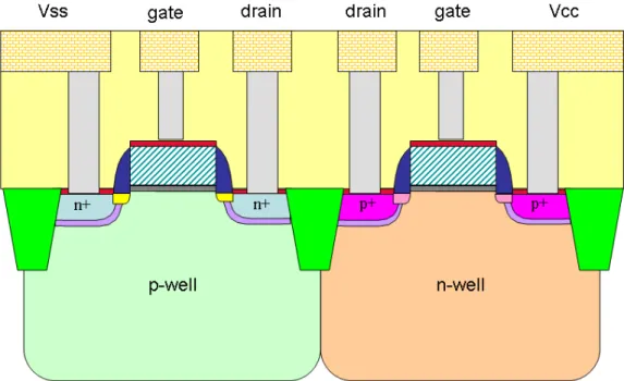
This work focuses on the complementary metal oxide semiconductor (CMOS) device. The CMOS is constructed using the p channel MOSFET (PMOS) and n channel MOSFET (NMOS). Figure 1-8 is a schematic illustration of the cross-sectional structure of the CMOS; the left side is an NMOS transistor and the right side is a PMOS transistor. The source side of the NMOS transistor connects to Vss. The drain site of the NMOS transistor pulls down to Vss level when the NMOS gate switches on. Conversely, the source side of the PMOS transistor connects to Vcc. The drain site of the PMOS transistor pulls up to Vcc level when the PMOS gate switches on; that is, the main function of the PMOS transistor is to transmit the Vcc signal and the NMOS transistor transmits the Vss signal. Thus, a CMOS chip transmits a Vss or Vcc signal through the logic operation of transistors. The advantage of CMOS technology is low power consumption. During their operating period, diodes remain in the reverse bias condition and consume energy only during the switching period.
The main function of a CMOS is to transmit a high or low signal through the logic operation. The components of the CMOS can be split into six nodes types—the n+/p-well node, NMOS gate node, p-well node, p+/n-well node, PMOS gate node, and n-well node.
From the perspective of electrical characteristics, the function of the NMOS gate node and PMOS gate node is similar; that is, each acts as a top plate of a capacitor and should resemble a high-resistance node. Thus, the NMOS gate node and PMOS gate node can be considered the same. The function of the p-well and n-well is to provide the source side of NMOS and PMOS transistors. The resistance of these two nodes is very low, such that they can be put into the same group before the manufacturing process is completed. For CMOS technology, CMOS components can be grouped into four node types—the n+/p-well node, gate node, p+/n-well node, and well node. The goal of defect isolation is to recognize these four nodes via a failure analysis process.
1.3.2
Static random access memory (SRAM)
SRAM is the memory that always stores the data in bit cells while chip power maintained. It does not need to re-write within a period, as does the dynamic random access memory (DRAM). Additionally, SRAM has the high-speed read and write capabilities and is adopted widely in central processing unit (CPU) chips. In modern integrated circuit (IC) manufacturing, SRAM is a leading product and the vehicle for advanced technology development [9]. However, the bit cell area of SRAM is larger than that of DRAM, meaning its manufacturing cost is higher.
A DRAM bit cell is composed of a transistor and capacitor. An SRAM bit cell is composed of six transistors—four NMOS transistors and two PMOS transistors. Figure 1-9(a)
shows the circuit of an SRAM bit cell. The role of PMOS transistors is to increase the signal to the Vcc level and is annotated as the pull up (PU) in the circuit. Conversely, the role of the NMOS transistor is to pull down the data to the Vss level, and is annotated as the pull down (PD) in the circuit. The PU and PD transistors are arranged in a latch circuit to retain data in the cell. The remaining NMOS transistors are called pass gate (PG) transistors, which control read and write timing. Figure 1-9(b) shows the layout pattern of the SRAM bit cell.
The failure mode of the SRAM bit can be identified via electrical testing. Since SRAM is a kind of CMOS chip, its power consumption is low while operating. Thus, the standby current (Isb) of SRAM should be low and this Isb will be tested at the start of the test process. Even though electrical testing can locate the exact bit failure location, a further isolation process is still necessary for cause identification. Such a failure analysis procedure includes using SEPC to isolate any possible high resistance or gate oxide rupture in a bit cell. If no abnormality were found via SEPC analysis, a nano probe tool is applied to measure the electrical performance of transistors [10].
1.3.3
Lateral double diffused metal oxide semiconductor (LDMOS)
According to Moore’s law, the transistor counts will double every 1.8 years. The dimensions of transistors must also decrease according to this law. With the scalability and cost savings for manufacturing, CMOS technology is widely used for digital circuits. However, the world remains analog. Digital processing should be converted back to analog
efficiently. Thus, the lateral double diffused metal oxide semiconductors (LDMOSs) were developed to reduce manufacturing costs and increase flexibility in high-voltage and high-current applications (e.g., power management ICs, displays, motor drivers, and class-D amplifiers) [11,12,13].
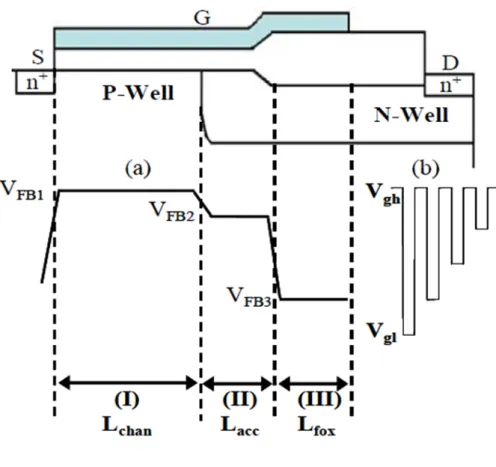
Figure 1-10 shows the cross-sectional structure of the lateral double diffused negative metal oxide semiconductors (LDNMOSs) [13]. In this cross section, the n-well was used as the extended drain side to sustain high power and the p-well was the body site of the device. Channel length, Lchannel, is the area where the p-well and poly gate overlap, and is controlled by the physical locations of the active area, the poly gate, n-well, and p-well. In this work, the mismatch mechanism of a current mirror composed of lateral double diffused positive metal oxide semiconductors (LDPMOSs) is investigated via in situ SEPC inspection. The SEPC inspection method identified a misaligned p-well mask, causing Lchannel variation and deviation of transistor saturation current from the target value.
1.4 Overview of defect isolation by SEPC
As the dimensions of transistors are scaling, the demand for an inspection tool with good spatial resolution has increased. Moreover, the transistor number of a VLSI containsbillion of transistors, indicating that this inspection tool should be able to analyze as many transistors as possible. With the improvements of electron guns and reduction of aberrations, SEM image resolution has improved to the nm scale and with a large view field. Additionally, the
secondary electron in SEM is sensitive to the voltage distribution of the inspected surface, facilitating inspection of high-resistance defects on ICs [14-16]. The contrast phenomenon arises from the influence of surface potential, and is called SEPC, or voltage contrast (VC) [17].
The SEPC effect was first observed in 1941 by Knoll [18]. Hardy et al. characterized SEPC with a voltage precision of 50 mV in the range of -30–30 V [19]. Aton et al. and Manhant-Shetti et al. demonstrated that standard SEM can isolate continuity failure of a special IC test pattern [20, 21]. The detection limit was 2 × 10¹¹ Ohm [21]. Sakai et al. biased the test pattern to lower the detection limit to 1 × 10⁴ Ohm [22]. Colvin utilized SEPC to isolate gate oxide leakage [23]. The SEPC arises from surface potential after electron beam irradiation [24]. This method has a contactless capability in voltage investigations and has been adopted for IC debugging [25].
1.5 Overview of dopant profiling by SEPC
Modern microelectronic IC technology enhances the performance of transistor through scaling down of transistor [5, 6]. The distribution and concentration of dopant is the key to enhance device performance when developing nano-scale devices. With a sensitivity from 1016 to 1020 cm-3 and a spatial resolution of 10 nm, the SEPC effect in SEM has emerged as the potential method for dopant profiling [26, 27]. In addition, SEPC arise from the built-in potential across the diode, indicating this is an electrical measurement method which collects
active dopant signal only [27].
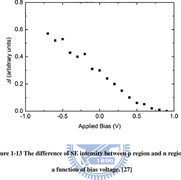
The dopant contrast in SEM was first observed in 1967 by Change and Nixon [28]. After that, researchers have been investigating the dopant contrast mechanism and each group has proposed its own proposal. Pervoaic et al. and Turan et al. proposed that surface potential determines secondary electron emission rate [29, 30]. Sealy et al. and Muzzo et al proposed that a patch field outside the specimen is a major factor in dopant contrast [31, 32]. Figure 1-11 shows the simulation result that the built in potential initiates an electrical field outside the specimen [32]. The electrical field will repel electron out the p-type node, but attract electron back to specimen in n-type node, resulting the brightness and darkness contrast in p type node and n type node, respectively. Hsiao et al. observed that the strain effects will influence dopant contrast [33]. Elliott et al. and Venables et al. reported that the SEPC profile of a p+/n-well junction shows a linear relationship with the logarithm of the SIMS depth profile and their results are shown in Figure 1-12 [26, 27]. SIMS is a dopant profiling tool by collecting the all dopant elements no matter is it an active dopant or not. Figure 1-13 shows the Elliott’s study on a biased junction [27]. Elliot found that the SEPC intensity is proportional to the biased voltage, indicating the surface potential determines the secondary electron emission rate [27].
1.6 Overview of dopant profiling techniques
SIMS is an analytical tool with high sensitivity and a wide dynamic detection range. The tool sputters the specimen surface using a primary ion beam and measures the elements using a mass spectrometer. The SIMS detection limit is 1012–1016 cm-3, and depends on material type [34]. With careful calibration of sputtering rate and low primary ion energy, SIMS has been used widely to characterize the depth profile of shallow junctions in CMOS devices [35]. However, SIMS is a destructive analytical method that depicts the dopant profile by sputtering the analytical target to mass spectrometer. All sputtered elements will be guided to the mass spectrometer and counted in the depth profile. Target dimensions should be larger than 50 × 50 µm, meaning that SIMS cannot be applied in the site-specific real circuit.
1.6.2
Scanning capacitance microscope (SCM)
SCM is a scanning probe microscope that uses a tiny tip to scan a specimen and record the capacitance response. Williams conducted the two-dimensional dopant profiling via SCM with a 10 nm spatial resolution [36]. A high-quality oxide should be grown in a specimen’s surface for reliable measurement, making the repeatability of SCM poor for many samples. Figure 1-14 shows schematic to illustrate the SCM operation principle [36].
1.6.3
Kelvin force probe microscope (KFPM)
KFPM combines AFM and SCM to map the electrostatic voltage difference between the tip and specimen surfaces [37]. The electrostatic force between the tip and specimen under a constant range, Z, is given by
dZ dC F =1/2 V2
……….(1)
where C is coupling capacitance and V is electrostatic voltage between the tip and specimen [37]. Surface potential is determined as measured electrical force, coupling capacitance, and tip potential. Figure 1-15 shows the KFPM system [37].
1.6.4
Electron holography
Electron holography is also a surface potential mapping method that uses interference of an off-axis electron beam in transmission electron microscope (TEM) [38]. With improved spherical aberration and a field emission gun, Griyelyuk et al. reported a 2D diode potential mapping with a spatial resolution of 6 nm and voltage sensitivity of 0.17 V [39]. However, an accurate potential map requires a sample with uniform thickness, such that electron holography is rarely used in IC manufacturing.
1.6.5
Chemical delineation
Chemical delineation uses acids to etch heavily doped areas selectively [40]. The silicon surface is first oxidized to silicon dioxide (SiO2) by nitric acid and then dissolved into a solution by fluride acid. The etching rate is limited by the concentration of holes in the sample surface [41]. The etching rate of n+ Si can be enhanced by band bending in solution, accumulating holes in the n+ surface. The etching rate of p+ silicon can be enhanced by anodic biasing, creating holes in the p+ surface [42]. However, this method has difficulty identifying the precise well profile due to low dopant dosages. Further, wet etching methods are
destructive, meaning that the doping area will be etched out permanently.
1.7 Motivations of study
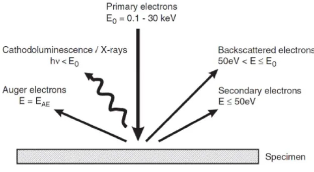
Transistors are built with solid materials and using their semiconductor electrical properties to perform complex computations. SEM has been widely used to inspect physical and electrical transistor properties. For instance, people use the secondary electron (SE) to measure transistor dimensions, use the backscattered electron (BSE) to inspect element contrast, and use the Auger electron and X-rays for element analysis. The SE contrast, which arises from the differences in surface potential, is called SE potential contrast (SEPC) and can be used to inspect electrical transistor properties. The SEPC has been widely applied in electrical defect isolation and dopant profiling.
Even though experimental results demonstrate that SEPC is an efficient method for continuity failure isolation, failure mode of an IC is not just a continuity issue. Four node types are used in VLSI chips, polysilicon gate node, n+/p-well node, p+/n-well node, and well nodes [43]. The traditional SEPC method cannot distinguish between all node types. This study investigates the SEPC by varying primary electron energy and discusses the source of potential contrast without additional biasing. Finally, this study offers a procedure to distinguish between different nodes in a chip.
In application of dopant profiling, many studies have applied SEPC for electrically active dopant profile mapping [31, 32]. However, as the device has nano-scale dimensions, the study
of SEPC in real circuit is rarely reported. The spatial resolution, site-specific analytical capability and poor SEPC signal in small bandgap material are emerging as the top three issues in SEPC method [44, 45]. Jepson et al. observed that the SEPC spatial resolution is improved in helium ion microscopy (HeIM) [46, 47]. Kazemian et al study of using focused ion beam (FIB) on sample preparation to meet the requirements for site-specific analysis [48]. However the SEPC is significantly reduced due to the damage layer generated by FIB, as shown in Figure 1-16 [48]. Hence, this study fills the gap in the literature by enhancing dopant contrast with nano-probe assistance. In addition, author converts the SEPC image to a voltage scale and elucidates theoretical description about the device physics [49-51].
1.8 Organization of the thesis
In chapter 1, the CMOS technology revolutions and process characterization challenges are introduced. We also have brief overview of the physical and electrical properties of the pn diode. The applications of CMOS technology in the logic circuit, SRAM, and LDMOS are also addressed in chapter 1. Additionally, the overview of defect isolation and dopant profiling using SEPC, and techniques for dopant profiling are also summarized in chapter 1. In chapter 2, the experimental instruments, sample preparation methods, electrical and physical characterization techniques are presented. This chapter introduces the secondary electron in SEM, sample milling tool FIB, electrical measurement tool nano-probe system and AFM.
A procedure is suggested to distinguish all node types in chip. Finally, this new procedure is applied in a real case and isolates defect successfully. Next, in chapter 4, the sample preparation methods for SEPC in dopant contrast inspection are examined. And a application of SEPC in p+/n-well junction leakage is presented. In chapter 5, this chapter investigates the use of SEPC with an in-situ nano-probe biasing to examine a silicon p+/n-well junction. The SEPC image is digitalized to elucidate the physics of diode. In Chapter 6, the mismatch mechanism in a current mirror was investigated using a SEM with in-situ nano-probe biasing. In Chapter 7, we summarize the experimental results and give a conclusions and suggestions in future works.
Figure 1-3 (a) Band gap diagram of p-type and n-type semiconductors. (b)
Figure 1-4 (a) The space charge distribution of a linearly-graded junction.
(b) The electrical field of the junction. (c) The electrical potential of the
Figure 1-5 (a) The band diagram of a diode under thermal equilibrium. (b)
The band diagram of a diode in forward bias condition. (c) The band
Figure 1-7 (a) The radiation mechanism of a forward biasing diode. (b) The
Figure 1-8 Schematic illustrats the cross-sectional structure of the CMOS
Figure 1-9 (a) The circuit of a SRAM bit cell. (b) The layout pattern of a
Figure 1-10 The cross-sectional structure of the lateral double diffused
Figure 1-11 The simulation result of electrical field above the unbiased SiC
Figure 1-12 (a) SEPC image on a Si test structure. (b) SEM contrast profile.
Figure 1-13 The difference of SE intensity between p region and n region as
Figure 1-16 The SEPC images prepared by different methods (a) The
cleaving result. (b) The polishing result. (c) The FIB milling result. (d)
Chapter 2
Techniques
2.1 Sample preparation process
2.1.1
Planar sample preparation
The purpose of sample preparation is to make the specimen ready for physical and electrical characterization through mechanical and chemical treatment. In this work, the specimen is an IC chip with one poly layer and five metal layers. Planar sample preparation is using mechanical polish method to approach the target layer. The specimen is polished to contact layer for electrical measurement by nano-probe system or AFM. The mechanical polishing tool used in this work is Allied MultiprepTM and its picture is shown inFigure 2-1(a) [52]. Figure 2-1(b) shows diamond films with different color to indicate different abrasive effect [52]. The diamond film is changed from coarse to fine for minimizing the scratch in specimen surface.
2.1.2
Cross section sample preparation
The Allied MultiprepTM is also can be used in cross-section sample preparation after changing the polish head. Figure 2-1(c) shows the polish head for corss-section sample preparation [52]. In this work, the specimen is prepared in cross-section for dopant profile inspection.
2.1.3
Chemical delayer and Ar sputtering
The disadvantage of mechanical polish method is that it generates a damaged layer on the specimen surface, hindering the SEPC inspection. Chee et al reported that the chemical solution containing 40% NH4F can remove the oxide layer in Si surface and passivate the silicon surface [53]. Our study also confirms the BENEFIT effect of NH4F treatment in SEPC inspection [54]. For active area inspection, using HF solution is the most effective way for dielectric layer removing. In this work, the HF solution is used to remove the oxide layer above the active layer. In addition to chemical treatment, the Ar sputtering is also used to minimize the damaged layer thickness resulting from mechanical polishing. The apparatus we used in this work is Gatan Model 693.
2.2 Material analysis
2.2.1
Scanning electron microscope (SEM)
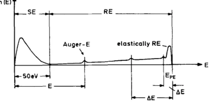
SEM was a primary electron beam to scan the specimen surface and collects the ejected electron by detector. The SEM model in this work is Hitachi S4700, which using field emission gun in primary electron beam generation. The interactions of primary electron beam with specimen generates characteristic signals like secondary electrons (SE), backscattered electrons (BSE), Auger electrons, and X-ray, and as shown in Figure 2-2 [17]. Figure 2-3 shows the distribution of emitted electrons after the bombardment of primary electron beam. [24]. The secondary electron is the inelastic collision result between primary electron with
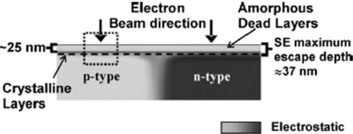
specimen and it is energy is smaller than 50 eV. On the contrary, backscattered electron is result from the elastic collision and its energy is close to the primary electron energy. Since the secondary electron energy is small, its escape depth is close to the surface, about 37 nm [48]. Figure 2-4 shows the escape depth of Si diode with FIB sample preparation [48]. The spatial resolution of the SEM is determined by the probe size of SEM. The specification of S4800, the upgrade model of S4700, possesses a 2 nm spatial resolution at 1 keV [56].
Since the energy of SE is less than 50 eV and majorly distributes at 4 eV, making SEM contrast with high correlation to the specimen surface potential [24]. SEPC shows lower contrast with positive potential. The traditional SEPC uses the fixed primary electron energy at 1 keV to isolate the continuity failure in IC [23]. The source of specimen surface potential comes from surface charging after electron irradiation [24]. Figure 2-5 shows the schematic to illustrate the surface charging effect [24]. The SE yield (δ) is the division of emission electron number by injection electron number.δ > 1 results in positive charging in the surface and negative charging when δ < 1. Table 2-1 shows the δ and maximum primary electron energy EPEm for CMOS materials [24]. The traditional SEPC condition 1 keV will result a positive charging in the specimen. In this work, we uses EPE =5 keV to make a negative charging in the specimen. The sample was polished to contact layer and irradiate by 1 keV and 5 keV electron beam, respectively. The SEPC images of contacts were recorded and a discussion is made to explain to contrast behavior. The second part of the thesis investigates SEPC with in-situ
nano-probe biasing to examine 2D dopant profile inspection. The dopant contrast is enhanced by nano-probe biasing and a series image process work is made to elucidate the physics of device.
The spatial resolution for SEPC is limited by the probe size of the inspection tool. Castell et al have suggested a 0.1 nm probe size of SEM for dopant mapping on the nanotechnology age [6]. In this work, the spatial resolution of S-4700 is about 2 nm. Recently Helium Ion Microscopy (HeIM) is a new tool with probe size that is as small as 0.25 nm. Jepson et al have reported SEPC mechanism in HeIM is similar to SEM [46, 47]. Their further inspections observed that the SEPC spatial resolution is improved in HeIM, making HeIM an ideal candidate for nano-scale dopant mapping in the future [46, 47].
2.2.2
Focused ion beam (FIB)
The operation of FIB is similar to SEM, which uses a focus ion beam to image the specimen instead of focused electron beam used in SEM. The interaction between ion beam and specimen also generates secondary electron and could be used to form an image. Additionally, the mass and momentum of ion is far more than electron, FIB will sputter the specimen surface and be a precision milling tool. The FIB apparatus used in this work is FEI DB235. Figure 2-6 shows the precise cross-sectioned milling capability of a FIB [56].
2.3 Electrical analysis
2.3.1
Nano-probe system
The nano-probe system is a transistor level electrical measurement tool. The nano-probe system in this work is DCG sProber, which equipped four positioners with 2 nm resolution of movement [57]. The sProber can be installed into the existing SEM and FIB for cost saving. As the transistor dimension going into nano-scale dimension, the major challenges of nano-probe system are the how small of tip size can be made and how many tip counts can be put in a small area. Figure 2-7(a) shows the DCG nProber which with 8 nano positioners [58]. Figure 2-7(b) is a SEM image from nProber, showing the 8 nano tips probe in the metal 1 layer of SRAM [58]. The tip radius is smaller than 50 nm [57]. The DCG’s system also has anti-contamination function for offering a low resistance measurement [57].
The major application of a nano-probe system is to measure the electrical characteristic of a transistor. Because the transistors are covered by metal layers and passivation layer, the sample was polished to contact layer for electrical measurement. In this work, the nano tips probe on the contact to measure the Id-Vg curve of the LDMOS. In addition, nano-probe was used to bias the n-well and p-well in a reverse bias condition, enhancing the SEPC effect in SEM. The missing dopant contrast is restored after the bias is triggered on the diode nodes, offering a new application of nano-probe system.
proposed bitcell pulsing measurement method to isolate the defective transistor of the SRAM [58]. Other applications include using electron beam induced current (EBIC) to characterize the carrier life time and electron beam absorption current to isolate the continuity failure of backend metal layers [57]. However, the electron beam irradiation may cause transistor degradation and the primary electron beam energy should be as low as possible.
2.3.2
Conductive atomic force microscope (C-AFM)
AFM uses a tiny tip to scan the specimen surface and record the atomic force interaction between tip and specimen [59, 60], including electrostatic force, van der waals force, and magnetic force…[59, 60]. Since the AFM has the atomic scale resolution, the AFM is widely adopted to measure the electrical properties, magnetic properties, and topology information of the specimen. The operation modes of AFM have non-contact mode, contact mode, and tapping mode. Figure 2-8 shows the schematic to illustrate the operation principle of a C-AFM [61].
The model of AFM in this work is Veeco Innova. The Innova is a contact mode AFM which using a metal tip to measure the conductivity of specimen. The measuring current ranges from 2 pA to 1 µA. In this work, C-AFM was used to isolate the leakage p+
/n-well junction. The current map of C-AFM result indicates the leakage p+/n-well junction appeared in every alternative row. The misalignment of the p-well mask layer is identified as the root cause of leakage.
With high sensitivity in electrical measurement, C-AFM can be used to isolate high resistance issues and small leakage issues in CMOS technology. A four tips C-AFM system was also developed to measure the transistor’s electrical characteristic. The benefit of transistor measurement by C-AFM is no damage of transistor due to the electron beam irradiation. However, without the assistance of SEM, the transistors’ location is located by the scanning of tips. For soft material like copper, the scratch induced by the tip may initiate unwanted short path between metals, limiting the application in the metal layer probing.
Figure 2-1 (a) The polish mechine Allied MultiprepTM. (b) Diamond films
with colors to indicate different abracive effect. (c) The polsih head for
Figure 2-2 Schematic drawing indicates characteristic signal generated by
Figure 2-3 Schematic drawing shows the distribution of emitted electrons
Figure 2-4 Schematic drawing shows the escape depth of silicon diode with
Figure 2-5 Secondary electron yield (
δ) versus primary electron energy E
PE.
Table 2-1 The maximum secondary electron yield (
δ
m) and maximum
primary electron energy (E
PEm
Figure 2-7 (a) DCG nProber with 8 nano positioners. (b) SEM image
Figure 2-8 Schematic drawing shows the operation principle of C-AFM.
Chapter 3
SEPC in contacts by SEM primary electron
energy adjustment
3.1 Introduction
With the assistance of electronic design automation (EDA) software and the demanding of chip functionality, the number of transistors in a VLSI chip can exceed billions. However, a tiny defect in a transistor can cause malfunction of the entire chip. An efficient fault isolation method is important to maintaining product with high yields and performance. The SEPC method is widely used to isolate connectivity failures and gate oxide ruptures in VLSI chips [22, 23]. The SEPC effect is correlated to the surface potential of the area of interest [20, 21]. For CMOS technology, four contact nodes are used—the n+/p-well node, p+/n-well node, poly gate node, and well node [15, 43]. The conventional SEPC method uses a low EPE=1 keV [62, 14]. However, a low EPE cannot distinguish between these four node types. For instance, the contrast between p+/n-well nodes and well nodes is with the same brightness under the low EPE condition, indicating that traditional SEPC cannot detect p+/n-well junction leakage to wells. In this work, primary voltage adjustment is applied to overcome this limitation.
3.2 Experimental details
In this experiment, the sample is a functional SRAM manufactured using 0.15 µm technology. A p-type (100) Si wafer with 8–12 Ohm-cm resistivity was the substrate. The
sample was processed with the standard CMOS process up to the Metal 3 layer.
All SEM images were obtained with a Hitachi S4700 equipped with an (E×B) filter. Figure 3-1 illustrates the E×B filter function. The typical SE energy was <50 eV [24]. The E×B filter removes the high-energy tail of the BSE and guides the SE to the upper detector to enhance the SEPC effect on Si. The SEM operating conditions were optimized for diode visualization. The SEPC image was obtained using an EPE of 1 keV and 5 keV. The SRAM chip with normal function was fabricated and manually polished contac for SEPC inspection. Notably, a FIB from FEI DB235 was used for cross-sectional inspection.
3.3 Results and discussion
3.3.1
SEPC result by primary electron energy adjustment
Two functional SRAM samples were polished to contact layer and the SEM image was acquired with 1 keV and 5 keV EPE, respectively. Figure 3-2 shows the SEM image with 1 keV EPE. In this image, the contrast of the contact can be classified into three levels. The contrast of the polysilicon contact, n+/p-well contact, and p+/n-well contact shows the low contrast, moderate contrast and high contrast, respectively. Figure 3-3 shows the SEM image obtained with 5 keV EPE. Contrast in the image also has three levels, but differs trend from that of Fig 3-2. The contrast of the polysilicon contact, n+/p-well contact, and p+/n-well contact shows the high contrast, low contrast and moderate contrast, respectively. Contrast with different EPE values behaves differently.
The SEPC arises from different surface potentials after primary electron (PE) irradiation. The source of surface potential is the yield of the SE, which is not equal to that of the primary electrons. SE yield (δ) is the dividing of SE number by PE number. Figure 3-4 shows the tungsten SE yield (δ) as a function of EPE [24]. The surface potential will be positive charging when the SE yield is larger than 1, and negative charging when the SE yield is < 1. Based on Seiler’s study, the tungsten surface will be positive charging at EPE=1 keV and negative charging at EPE=5 keV [24].
Figure 3-5(a) is a schematic showing the contrast behavior when EPE is 1 keV. According to the traditional SEPC effect, when a sample was exposed to the 1 keV electron beam, a positive charge was generated on the sample surface. On a floating contact, such as a polysilicon contact, the positive charge remained on the surface, and reduced the number of SEs collected by the detector. Thus, the polysilicon contact has low contrast in the SEM image. For a positive charge, the p+/n-well is forward biased, such that the positive charge can be discharged through the p+/n-well to the substrate. Therefore, the p+/n-well contact will be in a higher contrast. Conversely, the n+/p-well is reverse biased for the positive charge. Thus, positive charges are seldom discharged through the n+/p-well to the substrate and remain on the surface of the contact connected to the n+/p-well, such that the contact on n+/p-well will be lower contrast. For the grounded contact, the positive charge will be discharged to the substrate, and will not reduce the number of SEs collected by the detector. Thus, the grounded
contact is brighter than the floating contact in the SEM image.
Figure 3-5(b) shows a schematic explaining contrast behavior when EPE is 5 keV. A negative charge will result on the sample surface (Fig. 3-3). Under this negative charging condition, the negative charge will be maintained on the polysilicon contact surface and the number of SEs collected by the detector will increase; the polysilicon contact is bright in the SEM image. For negative charging, the p+/n-well is reverse biased, and the negative charge cannot be discharged easily through the p+/n-well; thus, the p+/n-well contact will have high contrast. The n+/p-well contact is forward biased for the negative charge, such that the negative charge can be discharged through n+/p-well to the substrate. The n+/p-well contact will be low contrast in SEM image. For a grounded contact, the negative charge will be discharged to the ground and will not increase the number of SEs collected by the detector; thus, the grounded contact is darker than the floating contact in the SEM image.
Table 3-1 summarizes the contrast behavior of contacts under the 1 keV and 5 keV EPE conditions. According to table 3-1, identifying the defective contact is easy when SEM images were acquired under both 1 keV and 5 keV.
3.3.2
Application of primary electron energy adjustment in defect
isolation
The sample is a 0.15-µm SRAM chip that suffers a single bit failure. The sample is planar polished to Metal 1 layer for SEPC inspection to find any abnormality in the Metal 1
layer. Figure 3-6 shows the SEM image under 1 keV EPE. However, no abnormality was identified in the SEM micrograph. Thus, EPE was increased to 5 keV and another SEM micrograph was acquired, as shown in Fig. 3-7. One C-shaped Metal 1, which acts as the storage node of SRAM, is significantly brighter than the other C-shaped Metal 1. Thus, a cross-sectional inspection is performed by FIB, which reveals a porous n+/p-well contact in the failing cell, as shown in Fig. 3-8.
The abnormal SEPC from this sample cannot be identified at EPE=1 keV because three contacts are under Metal 1 layer: one connected to the p+/n-well another connected to the n+/p-well, and the last connected to polysilicon. When the sample is exposed to a 1 keV EPE condition, positive charges were generated on the sample surface. According to the principle of SEPC described previously, positive charges can be discharged by the contact connected to the p+/n-well. Thus, each Metal 1 can discharge its positive charges via its normal contact to the p+/n-well and all Metal 1 SEPC would be normally bright. In this case, the defect was an open contact connected to the n+/p-well. Therefore, one cannot detect this defect by EPE=1 keV. Conversely, negative charges will be generated on the sample surface when the sample is exposed to EPE=5 keV. Negative charges will be discharged by the normal n+/p-well contact for all normal cells except the open contact. Thus, the negative charges were not discharged on abnormal cells, and would increase the number of SEs collected by the detector; thus, abnormal C-shaped Metal 1 was brighter than other metals. With the EPE=5 keVcondition,
this defect may be identified because high resistance located on n+/p-well contact cannot be identified when EPE=1 keV.
3.4 Summary
In summary, the SEPC exhibits different contrast effects by adjusting the primary electron energy. The proposed SEPC procedure can distinguish between all contact types in an SRAM chip, overcoming the weakness of traditional SEPC. The SEPC images under varying primary electron energies were acquired experimentally and discussed. The surface-charging model explained the contrast behavior well. Finally, the proposed SEPC procedure was applied to isolate a porous n+/p-well contact, which cannot be found via the tradition SEPC method.
![Figure 1-2 Logic technology node and transistor gate length over time. [2]](https://thumb-ap.123doks.com/thumbv2/9libinfo/8060071.162922/41.892.142.785.130.607/figure-logic-technology-node-transistor-gate-length-time.webp)
![Figure 1-11 The simulation result of electrical field above the unbiased SiC junction surface due to the built-in potential [32]](https://thumb-ap.123doks.com/thumbv2/9libinfo/8060071.162922/50.892.132.712.188.616/figure-simulation-result-electrical-unbiased-junction-surface-potential.webp)
![Figure 1-15 Schematic illustrates the KFPM operation principle. [37]](https://thumb-ap.123doks.com/thumbv2/9libinfo/8060071.162922/54.892.128.726.157.540/figure-schematic-illustrates-kfpm-operation-principle.webp)
![Figure 2-5 Secondary electron yield (δ) versus primary electron energy E PE . [24]](https://thumb-ap.123doks.com/thumbv2/9libinfo/8060071.162922/67.892.137.797.188.704/figure-secondary-electron-yield-versus-primary-electron-energy.webp)
