國立臺灣大學電機資訊學院電子工程學研究所 碩士論文
Graduate Institute of Electronics Engineering College of Electrical Engineering & Computer Science
National Taiwan University Master Thesis
應用於生醫訊號偵測系統之低功耗前端電路
A low power Analog Front-end for Bio-signal Monitoring System Application
陸舜東 Shun-Tung Lu
指導教授:呂學士 博士 Advisor: Shey-Shi Lu, Ph.D.
中華民國 101 年 7 月
誌謝
研究所兩年的生涯在此畫下句點,最要感謝的人就是指導教授呂學士老師。
老師開啟了我對電路研究的一扇窗,並提供給實驗室優良且充足的研究資源,讓 我能順利的做好我的研究。老師在做研究的態度以及待人處世之道亦是值得我學 習的對象。此外,更要感謝老師的推薦,讓我能夠到美國貝爾實驗室實習一年,
非常感謝您對我的肯定。
感謝孫台平教授、孟慶宗教授和林佑昇教授在百忙之中抽空來當我的口試委 員,您們的寶貴意見使得本論文更加完善。
感謝邱弘緯教授、陳筱青教授及汪濤教授平時的指導,不管在電路模擬、量 測上都給了我許多寶貴經驗,有了你們使我對電路設計有更深一層的認識。
感謝冠廷學長對實驗室工作站的維護,您還要負責實驗室的帳務真是辛苦了。
感謝毓傑學長對實驗室的付出及對我的指導,你是實驗室的台柱,有了你才能讓 我在電路設計上不斷進步。也感各位博班學長:昆穎學長、柏宏學長、建宇學長、
浚彰學長及德軒學長,謝謝你們在我碩班期間對我的照顧。
感謝育如學姊,有了你在美國實習的經驗以及從中幫忙引薦,我才能有這機 會到來到美國,您的幫忙讓我萬分感謝。
感謝同屆戰友們,黃肯、伯偉、瀚文及凱皓,我們合力完成了從人體端量測 心電訊號,經由無線收發機到電腦端讓心電訊號即時顯現在電腦螢幕上的晶片,
並且在口試當天現場展演給口試委員們看,真的是非常有成就感。碩班兩年的日
出。很高興認識了你們,也很高興能和大家一起畢業。
感謝實驗室的學弟們,資偉、侑農、奕誠、詔彥、易霖和文鼎這一年來的幫 忙,很珍惜和大家在實驗室的時光。
感謝我的家人。碩班時常因為做研究、趕下線而晚回家,你們總是希望我在 全力以赴之餘,也叮嚀我不要忘了身體健康。一路上有你們的支持才會支撐我到 現在,由衷的感謝你們。
陸舜東 2012.8
應用於生醫訊號偵測系統之低功耗前端電路
研究生:陸舜東 指導教授:呂學士 博士
國立台灣大學電子工程學研究所
摘要
由於患有慢性疾病的患者越來越多以及老年化社會的來臨,現代社會對於個 人化遠距醫療照護的需求也越來越高。幸運的是,隨著半導體產業的快速發展以 及積體電路設計產業逐漸的成熟,用來感測及監測生理訊號的生物醫學晶片得以 被實現。開發一個無線生醫訊號偵測系統晶片來實現遠距醫療照護的服務是可行 的。這不僅能幫助人們預防得到疾病還能促進人們的健康,進而增進生活的品質。
根據衛生署所頒佈的資料,心血管疾病是國人的十大死因之一。因此,一個可以 應用在遠距醫療照護服務的心電訊號監測系統對於現今社會是有其需要的。為了 要實現一個心電訊號監測系統,處理類比生理訊號的類比前端電路在系統裡是扮 演關鍵性的電路區塊。本論文提出了兩種低功耗低雜訊的類比前端電路用來降低
雜訊的干擾以及提供多種放大倍率的選擇。兩個類比前端電路皆使用 TSMC
0.18µm 的製程技術來完成高性能的生物醫學晶片。
放大器。藉由斬斷技術,電流回授式儀表放大器的輸入相關雜訊為 90nV/ Hz,
而整個類比前端電路的輸入相關雜訊則是 1uV/ Hz 。為了要符合各種心電訊
號大小的偵測,此電路提供了從 36dB 到 54dB 各種不同的增益選擇。此類比
前端電路在 1V 的供應電壓下只消耗了 6uW。
第二,本論文提出了一個類比前端電路以及脈衝寬度調變電路。脈衝寬度調 變電路是做為類比前端電路及數位訊號處理電路之間的介面電路。此類比前端電
路的輸入相關雜訊為 80nV/ Hz。此外,本電路不僅提供四種從 30dB 到 50dB
不同的增益選擇,並且具有很高的輸出訊號擺幅。基於 1V 的供應電壓下,此
類比前端電路消耗了 8uW 而脈衝寬度調變電路則消耗了 5uW。
A low power Analog Front-End for Bio-signal monitoring system application
Student: Shun-Tung Lu Advisor: Dr. Shey-Shi Lu
Graduate Institute of Electronics Engineering National Taiwan University
Abstract
With the growing pains suffered from chronic disease and the coming of aging society, there is a highly demand on personal telehealth systems. Fortunately, due to the dramatic development of semiconductor technology and the IC design industries, biomedical chips can be developed for sensing and monitoring bio-signals. It is possible for us to develop a wireless bio-signal monitoring SoC to realize telehealth service. It not only help people prevent illness in advance but also benefit their health that would increase their quality of life. According to the information that announced by the Department of Health, cardiac disease is one of the leading causes of death.
Therefore, a wireless ECG monitoring system for personal telehealth service is needed. To realize an ECG monitoring system, the analog front-end is a critical circuit
interference and provide a multiple gain selection. Both of the analog front-end based on the TSMC 0.18µm technology are proposed to realize high performance biomedical ICs.
First, a current feedback instrumentation amplifier with a programmable gain amplifier for ECG signal detecting is proposed. By using chopper technique, the input-referred noise of CBIA is 90nV/ Hz and the overall AFE is 1uV/ Hz. It provides several gain selections from 36dB to 54dB to meet the requirement for ECG signal detecting. The analog front-end only consumes 6uW based on the 1V voltage supply.
Second, an analog front-end with pulse-width modulation circuit is proposed.
The pulse-width modulation circuit acts as an interface between analog front-end and digital signal processing circuit. The input-referred noise of the analog-front end is 80nV/ Hz. Besides, it not only provides four gain selections from 30dB to 50dB, but also has high output swing. Based on the 1V voltage supply, the analog front-end consumes 8uW and the pulse-width modulation circuit consumes 5uW.
List of Contents
List of Contents
Chapter 1 Introduction ... 1
1.1 Motivation ... 1
1.2 Thesis Organization ... 4
Chapter 2 ECG Signal and System Requirement ... 7
2.1 ECG Signal Introduction ... 7
2.2 A Wireless ECG Monitoring System ... 12
2.2.1 Analog front-end (AFE) ... 13
2.2.2 Analog-to-digital converter (ADC) ... 14
2.2.3 Digital signal processing circuit (DSP) ... 15
2.2.4 OOK transmitter (TX) ... 16
2.2.5 OOK receiver (RX) ... 18
2.3 Principle of Analog Front-End Design ... 19
Chapter 3 Fundamentals of Analog Front-End ... 21
3.1 Offset and Noise in CMOS Circuits ... 21
3.1.1 Offset... 21
3.1.2 Noise ... 22
3.2 Low-Offset and Low-noise Technique ... 26
3.2.1 Auto-zero technique ... 27
3.3 Sub-threshold conduction design ... 36
3.4 Instrumentation Amplifier ... 39
3.5 Proposed Instrumentation Amplifier ... 41
3.5.1 Current feedback instrumentation amplifier (CBIA) ... 41
3.5.2 Differential difference amplifier with resistive feedback ... 43
Chapter 4 A Current Feedback IA with a Programmable Gain Amplifier for ECG signal Detecting ... 45
4.1 Introduction ... 45
4.2 Circuits Architecture ... 46
4.3 Circuits Implementation ... 49
4.3.1 Current feedback instrumentation amplifier (CBIA) ... 49
4.3.2 Common mode feedback circuit (CMFB) ... 52
4.3.3 Low pass filter (LPF) ... 54
4.3.4 Programmable gain amplifier (PGA) ... 59
4.3.5 Clock generator ... 64
4.4 Simulation ... 65
4.5 Layout ... 75
4.6 Measurement ... 76
4.6.1 Die photo and PCB design ... 76
4.6.2 Measurement setup ... 77
4.6.3 Measurement result ... 80
4.6 Summary ... 88
List of Contents
Chapter 5 An ECG Signal Monitoring Analog Front-End with Pulse-Width
Modulation Circuit ... 91
5.1 Introduction ... 91
5.2 Circuits Architecture ... 92
5.3 Circuits Implementation ... 95
5.3.1 Programmable gain differential difference amplifier ... 95
5.3.2 Rail-to-rail amplifier ... 99
5.3.3 Filter ... 104
5.3.4 PWM Circuit ... 105
5.3.5 On-chip oscillator ... 111
5.4 Simulation ... 112
5.5 Layout ... 124
5.6 Measurement ... 125
5.6.1 Die photo and PCB design ... 125
5.6.2 Measurement setup ... 126
5.6.3 Measurement result ... 127
5.6 Summary ... 136
Chapter 6 Conclusion ... 139
References ... 143
List of Figures
List of Figures
Fig.1.1-1 Healthcare cost from1970 to 2007……….2
Fig.1.1-2 Block diagram of the ECG monitoring system………..3
Fig2.1-1 Ideal ECG signal………..………8
Fig. 2.1-2 Electrode placement of the limb leads………..9
Fig. 2.1-3 Vectors of limb leads and augmented limb leads………..9
Fig. 2.1-4 Electrode placement of the precordial leads………11
Fig. 2.2-1 Block diagram of the wireless ECG monitoring system……….12
Fig. 2.2.1-1 Architecture of the analog front-end………13
Fig. 2.2.2-1 Architecture of the analog-to-digital converter………14
Fig. 2.2.3-1 Architecture of the digital signal processing circuit……….15
Fig. 2.2.4-1 Architecture of the OOK transmitter………16
Fig. 2.2.4-2 (a) ASK modulation (b) OOK modulation………..17
Fig. 2.2.5-1 Architecture of the OOK receiver………18
Fig. 2.3-1 Frequency and amplitude characteristics of the bio-signals………19
Fig. 3.1.1-1 Amplifiers with offset (a) differential input voltage equal to input offset voltage forces output to zero, (b) output offset of an amplifier with
Fig. 3.1.2-1 Concept of signal interferes by noise………...22
Fig. 3.1.2-2 Noise spectrum of standard CMOS amplifier……… 23
Fig. 3.1.2.1-1 Representation of resistor thermal noise by a current source………..24
Fig. 3.1.2.1-2 Representation of MOSFET thermal noise by a current source………24
Fig. 3.2.1-1 Principle of Auto-zero technique (a) Phase 1, ϕ=1 (b) Phase 2, ϕ=0…27 Fig. 3.2.1-2 Noise spectrum of auto-zero technique………29
Fig. 3.2.2-1 Principle of Chopper technique and its operation in Frequency/Time domain………..………30
Fig. 3.2.2-2 Chopper modulation. ………..……….31
Fig. 3.2.2-3 Noise spectrum of auto-chopper technique………..32
Fig. 3.2.2-4 Ideal and non-ideal waveforms of chopper amplifier in time domain (a) Amplifier output (b) Demodulated amplifier output………..33
Fig. 3.2.2-5 Basic concept of charge injection………..……… 33
Fig. 3.2.2-6 Charge injection model of a chopper modulator……….34
Fig. 3.2.2-7 Residual offset caused by spike (a) Spike signal (b) Demodulation signal (c) Demodulated spike……….34
Fig. 3.2.2-8 Reduce charge injection effect by using transmission gate……….36
Fig. 3.3-1 gm/ID plot……….……….38
Fig. 3.4-1 Differential amplifier with resistive feedback……….39
Fig. 3.4-2 A three operational amplifiers based instrumentation amplifier………….40
Fig. 3.5.1-1 Schematic of the current feedback instrumentation amplifier (CBIA)…41 Fig. 3.5.1-2 Simplified schematic of CBIA………42
Fig. 3.5.2-1 Schematic of the differential difference amplifier (DDA)………...43
List of Figures
Fig. 3.5.2-2 Differential difference amplifier with resistive feedback………44
Fig. 4.2-1 Architecture of the CBIA with PGA………...46
Fig. 4.2-2 AC coupling circuit (HPF) ……….46
Fig. 4.2-3 Concept of the analog front-end with chopper technique………...47
Fig. 4.3.1-1 Simplified schematic of CBIA……….49
Fig. 4.3.1-2 Small signal half-circuit model of the simplified CBIA……….50
Fig. 4.3.1-3 Complete schematic of CBIA………..51
Fig. 4.3.2-1 Concept of CMFB with resistive sensing………52
Fig. 4.3.2-2 Schematic of current based CMFB………..54
Fig. 4.3.3-1 Unity gain Sallen-Key low pass filter………..55
Fig. 4.3.3-2 Comparison of gain responses of the three types low pass filter………57
Fig. 4.3.3-3 Butterworth low pass filter………58
Fig. 4.3.4-1 Programmable gain amplifier………59
Fig. 4.3.4-2 Differential difference operational transconductance amplifier………..60
Fig. 4.3.4-3 (a) Non-inverting amplifier (b) Non-inverting amplifier equivalent circuit………..………61
Fig. 4.3.4-4 (a) Buffer (b) Small signal model of the buffer………...62
Fig. 4.3.4-5 A differential difference operational transconductance amplifier with a buffer stage to realize a programmable gain amplifier………63
Fig. 4.3.5-1 Problem of clock overlapping………..64
Fig. 4.3.5-2 Non-overlapping clock generator………64
Fig. 4.4-2 AC response simulation of DDA………66
Fig. 4.4-3 AC response simulation of Low-pass filter……….67
Fig. 4.4-4 AC response simulation of CBIA with PGA………..67
Fig. 4.4-5 CMRR Simulation of CBIA with PGA………..68
Fig. 4.4-6 PSRR Simulation of CBIA with PGA………..………..68
Fig. 4.4-7 Noise response simulation of CBIA………69
Fig. 4.4-8 Noise response simulation of CBIA with chopper modulation…………70
Fig. 4.4-9 Noise response simulation at the output of LPF……….70
Fig. 4.4-10 Transient response simulation at the input modulation………71
Fig. 4.4-11 Transient response simulation at the output modulation………...72
Fig. 4.4-12 Transient response simulation at the output modulation (Partial enlarged detail) ………..72
Fig. 4.4-13 Transient response simulation at the output of LPF, and the output of PGA………..73
Fig. 4.4-14 Transient response simulation of non-overlapping clock………..73
Fig. 4.5-1 Layout of ECG monitoring system (Ver.1) ………75
Fig. 4.5-2 Layout floor plain of ECG monitoring system (Ver.1)………...75
Fig. 4.6.1-1 Die photo of ECG monitoring system (Ver.1)……….76
Fig. 4.6.1-2 PCB design of ECG monitoring system (Ver.1)………..76
Fig. 4.6.2-1 AC response measurement setup………..77
Fig. 4.6.2-2 Noise and Acm measurement setup………...78
Fig. 4.6.2-3 PSRR measurement setup………79
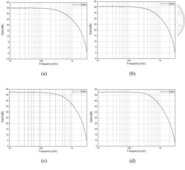
Fig. 4.6.3-1(a)(b)(c)(d) AC response measurement result of the AFE………81
List of Figures
Fig. 4.6.3-2 AC response measurement result of the AFE………..81
Fig. 4.6.3-3 CMRR measurement result of the AFE………...82
Fig. 4.6.3-4 PSRR measurement result of the AFE……….82
Fig. 4.6.3-5 DC gain of the AFE………83
Fig. 4.6.3-6 Input-referred noise spectrum of the CBIA in log scale (with and without chopper technique) ………84
Fig. 4.6.3-7 Input-referred noise spectrum of the CBIA in log scale (with and without chopper technique) ……….84
Fig. 4.6.3-8 Input-referred noise spectrum of the CBIA in linear scale (with and without chopper technique) ……….85
Fig. 4.6.3-9 Input-referred noise spectrum of the CBIA (before LPF)………85
Fig. 4.6.3-10 Input-referred noise spectrum of the CBIA (after LPF)……….86
Fig. 4.6.3-11 Input-referred noise spectrum of the AFE (after PGA)………..86
Fig. 4.6.3-12 Input-referred noise spectrum comparison of the AFE (after PGA) and CBIA (after LPF)………..………87
Fig. 4.6.3-13 ECG signal measurement result………..………...88
Fig. 5.2-1 Architecture of the AFE with PWM circuit………92
Fig. 5.2-2 Concept of the analog front-end with chopper technique………93
Fig. 5.3.1-1 Schematic of the differential difference amplifier (DDA)………95
Fig. 5.3.1-2 Equivalent small signal model of DDA………...96 Fig. 5.3.1-3 Implement an output chopper modulator in a single output amplifier….97
Fig. 5.3.1-4 Programmable gain differential difference amplifier with chopper technique………..98 Fig. 5.3.2-1 (a) Inverting amplifier (b) Non-inverting amplifier (c) Buffer…………99 Fig. 5.3.2-2 Common-mode input range of NMOS and PMOS input pairs………100 Fig. 5.3.2-3 Rail-to-rail input stage………100 Fig. 5.3.2-4 Common-mode input range of rail-to-rail input stage. The supply
voltage is larger than | Vgs,p | + Vgs,n + 2Vds,sat………101 Fig. 5.3.2-5 Common-mode input range of rail-to-rail input stage. The supply
voltage is smaller than | Vgs,p | + Vgs,n + 2Vds,sat……….101 Fig. 5.3.2-6 Transconductance (gm) versus Common-mode inputvoltage (Vin,CM) for rail-to-rail input stage. The supply voltage is larger than Vgs,p + Vgs,n + 2Vds,sat……….102 Fig. 5.3.2-7 Transconductance (gm) versus Common-mode input voltage for (Vin,CM) rail-to-rail input stage. The supply voltage is smaller than Vgs,p + Vgs,n + 2Vds,sat……….102 Fig. 5.3.2-8 Designing gm value to be constant………..103 Fig. 5.3.2-9 Schematic of rail-to-rail opamp………..104 Fig. 5.3.3-1 Second-order Butterworth low pass filter based on rail-to-rail opamp..104 Fig. 5.3.4-1 Block diagram of PWM circuit………..105 Fig. 5.3.4.1-1 Schematic of ramp wave generator……….106 Fig. 5.3.4.1-2 Wave function of Vctrl and Vout in ramp wave generator……….106 Fig. 5.3.4.2-1 Sample and hold circuit realize by (a) Simple NMOS switch
(b) Transmission gate switch (c) Bootstrapped switch………107
List of Figures
Fig. 5.3.4.2-2 On-resistance of the transmission gate switch………109 Fig. 5.3.4.2-3 Schematic of the bootstrapped circuit……….110 Fig. 5.3.4.3-1 Schematic of the rail-to-rail comparator……….110 Fig.5.3.4-2 Schematic of the SR latch………111 Fig.5.3.5-1 On-chip CMOS oscillator………111 Fig.5.4-1 AC response simulation of DDA………...113 Fig.5.4-2 AC response simulation of Rail-to-rail opamp………..113 Fig.5.4-3 AC response simulation of Low-pass filter………114 Fig.5.4-4 AC response simulation of programmable gain DDA………114 Fig. 5.4-5 CMRR Simulation of AFE………115 Fig. 5.4-6 PSRR Simulation of AFE………115 Fig.5.4-7 Input common mode range simulation of DDA……….116 Fig.5.4-8 Output swing simulation of DDA………116 Fig.5.4-9 Input common mode range simulation of Rail-to-rail opamp………117 Fig. 5.4-10 Transconductance (gm) simulation of the Rail-to-rail input stages……117 Fig. 5.4-11 Noise response simulation of AFE………..118 Fig. 5.4-12 Noise response simulation of AFE with chopper modulation………….119 Fig. 5.4-13 Noise response simulation at the output of LPF……….119 Fig.5.4-14 Transient response simulation of ramp wave generator………120 Fig.5.4-15 Transient response simulation of sample and hold circuit………121 Fig.5.4-16 Transient response simulation of comparator………121 Fig.5.4-17 Transient response interface simulation from AFE to PWM circuit (1)..122
Fig.5.4-19 Transient response simulation of on-chip oscillator………123 Fig.5.5-1 Layout of the ECG monitoring system (Ver.2) ……….124 Fig.5.5-2 Layout floor of the ECG monitoring system (Ver.2) ………124 Fig. 5.6.1-1 Die photo of ECG monitoring system (Ver.2)………125 Fig. 5.6.1-2 PCB design of ECG monitoring system (Ver.2) ………...125 Fig. 5.6.2-1 ECG signal monitoring setup……….126 Fig. 5.6.3-1(a)(b)(c)(d) AC response measurement result of the AFE……….127 Fig. 5.6.3-2 AC response measurement result of the AFE………127 Fig. 5.6.3-3 CMRR measurement of the AFE………128 Fig. 5.6.3-4 PMRR measurement of the AFE………129 Fig. 5.6.3-5 DC gain of the AFE………129 Fig. 5.6.3-6 Input common mode range of rail-to-rail opamp………130 Fig. 5.6.3-7 Input-referred noise spectrum of AFE in log scale
(with and without chopper technique)………131 Fig. 5.6.3-8 Input-referred noise spectrum of AFE in log scale
(with and without chopper technique)………131 Fig. 5.6.3-9 Input-referred noise spectrum of AFE in linear scale
(with and without chopper technique)………132 Fig. 5.6.3-10 Output waveform of the on-chip oscillator………..132 Fig. 5.6.3-11 Input-referred noise spectrum of AFE (before LPF)………133 Fig. 5.6.3-12 Input-referred noise spectrum of AFE (after LPF)………...133 Fig. 5.6.3-13 ECG signal measurement result (analog signal)………..134 Fig. 5.6.3-14 ECG and PWM signal………..134
List of Figures
Fig. 5.6.3-15 ECG and PWM signal (Partial enlarged detail) ………..135 Fig. 5.6.3-16 ECG signal measurement result (digital signal) ………..135
List of Tables
List of Tables
Table 2.1-1 Electrode label and placement………...8 Table 4.3.3-1 Second-order filter coefficients………..….…..57 Table 4.4-1 Summary of simulation result……….….74 Table 4.6-1 Summary of measurement result………..…89 Table 5.4-1 Summary of simulation result…………..………..123 Table 5.6-1 Summary of measurement result………..137 Table 6.1 Summary of measurement result……….……..140
Chapter 1 Introduction
Chapter 1 Introduction
1.1 Motivation
Due to the urbanization in modern society, the pressure and the fast pace of life may cause growing pains suffered from chronic disease. According to the information that announced by the Department of Health, cardiac disease is one of the leading causes of death. Besides, we are confronting to an aging society. More and more elderly people live alone without receiving a good medical care. All of these lead to a drive towards personal telehealth systems.
Another important reason for the demand on telehealth systems is that people consume more and more medical resource than ever before. Fig1.1-1 shows that healthcare cost has increased in all countries from past till now [12]. It reveals that the healthcare system in modern time needs to be changed.
A Low Power Analog Front-end for Bio-signal Monitoring System Application
Fig.1.1-1 Healthcare cost from1970 to 2007
Fortunately, with the dramatic development of semiconductor technology and the IC design industries, biomedical chips can be developed for sensing and monitoring bio-signals. It is possible for us to develop a wireless bio-signal monitoring SoC to realize telehealth service. It not only help people prevent illness in advance but also benefit their health that would increase their quality of life. In view of this, we decide to make a wireless ECG monitoring system.
The key requirements from such bio-signal monitoring systems are the extraction, analysis, and wireless transmission of the bio-signals with low-power consumption, and robust operation on removing noise artifact [9]. Fig1.1-2 shows the block diagram of ECG monitoring system, which is composed by an analog front-end, ADC, DSP, and transmitter. ECG signal has characteristics of the low-level and low frequency.
Thus, it is easy to be interfered with flicker noise, baseline drift and power line noise (60Hz). In order to lower the effect of such interference, a well-designed analog front-end is added as an analog process block, which is used to amplify and filter the ECG signal. Thus, it compensates some unwanted characteristics such as weak signals
This Work
Process 0.18um
Supply Voltage 1V
AFE Bandwidth:0.2Hz~400Hz Gain:36dB~54dB
SAR ADC 8.5-bits
OOK Transmitter
frequency:403 MHz output power:0 dBm
P1dB:-8 dBm
Power consumption
AFE 6.1 uW
SAR ADC 5.2 uW
DSP circuit 40.1 uW
OSC. 10 uW
OOK TX 2 mW/50 nW (on/off) Total Power 1.06 mW/61.4 uW(TX on/off)
V. 結論論與未來來應用
圖 40. 健康照護成本
本晶片是以 low-cost、real-time、可攜式 ECG 訊號分析的應用。一般醫院做 心電圖是偵測當下的心臟脈動;若若是需要長時間觀察心電訊號的患者,通常需要 患者住院觀察。此時,醫院需要顧用一個人負責觀測此人 real-time 的心電圖;
這個現象也同時透露露出醫療療品質與成本的問題,從圖 40 也可以大致看出此趨勢。
而本晶片設計的主軸也是為了了解決此問題,提出一個降降低醫療療成本與醫療療品質兼
Chapter 1 Introduction
and high noise to insure the purity of the ECG signal. In addition, analog front-end also provides a good driving ability for circuit system such as ADC in biomedical system. Hence, analog front-end is a critical circuit block having the function of signal arrangement in bio-signal monitoring system.
Fig.1.1-2 Block diagram of the ECG monitoring system
In this thesis, two kinds of low-power and low-noise analog front-end are proposed to lower the noise interference and provide a multiple gain selection.
Besides, it is common to use ADC circuit to digitalize the analog signal in traditional way. A pulse-width modulation (PWM) circuit is proposed to be another way that uses time-proportioning technique to represent the analog signal in time domain, and the digital circuit can use high-resolution counter to digitalize the signal. The proposed circuits have been implemented in TSMC 0.18µm 1P6M CMOS process and consume low power from a 1V supply.
1.2 Thesis Organization
The thesis is organized into six chapters.
Chapter 1 gives a brief introduction of this thesis.
Chapter 2 begins with a brief introduction of the ECG signal and then the ECG signal monitoring system is introduced. Finally, we focus on the introduction about the analog-front end for ECG signal monitoring application.
Chapter 3 begins with the discussion of noise and offset in CMOS circuits, then the low-noise and low-offset techniques such as auto-zero and chopper technique are introduced. The theory of chopper technique is especially discussed. In addition, sub-threshold conduction is also introduced in this chapter. Finally, some kinds of circuits in analog front-end are presented.
Chapter 4 presents a low-noise and low-power current feedback instrumentation amplifier with programmable gain amplifier. The chopper technique is used to reduce the noise in an amplifier. Some measurement setups for example AC response measurement and noise measurement are presented, and both simulated and measured results confirm the function of analog front-end.
Chapter 5 presents another low-noise and low-power analog front-end with pulse-width modulation circuit. The chopper technique is also used in this circuit.
Because of the difficulties to design a high resolution SAR ADC in such a low
Chapter 1 Introduction
voltage supply application and low-power consumption limitation, we proposed a pulse-width modulation circuit to act as an interface between analog front-end and digital signal processing circuit. Both simulation results and measurement results about the analog front-end and pulse-width modulation circuit are provided in this chapter to show that the performance of the circuit is good enough to detect ECG signals.
Eventually, the conclusions of this work are summarized in Chapter 6.
Chapter 2 ECG Signal and System Requirement
Chapter 2
ECG Signal and System Requirement
2.1 ECG Signal Introduction
Electrocardiogram (ECG/EKG) is a representation of electrical activity of the heart over a period of time, which is used in the analysis of heart disease. As the heart performs its function of bumping blood through the circulatory system, the result of action potentials within the heart would generate a certain sequence of electrical event.
A typical ECG signal consists of a P wave, a QRS complex, and a T wave, as Fig.
2.1-1 shows. This display indicates the overall rhythm of the heart and weaknesses in different parts of the heart muscle. By positioning electrodes on a patient’s skin in particular location, it is possible to extract useful information about the functionality of the heart. The placement of electrodes can form different ECG leads. There are 10
placement [31]. The electrode labels of RA, LA, RL, and LL form three limb leads and three augmented limb leads. The others electrode labels form six precordial leads.
Fig2.1-1 Ideal ECG signal
Table 2.1-1 Electrode label and placement
Electrode label Electrode placement
RA On the right arm or right shoulder LA On the left arm or left shoulder RL On the right leg or right thigh LL On the left leg or left thigh
V1 In the fourth intercostal space just to the right of the sternum.
V2 In the fourth intercostal space just to the left of the sternum.
V3 Between leads V2 and V4.
V4 In the fifth intercostal space in the mid-clavicular line.
V5 Horizontally even with V4, in the anterior axillary line.
V6 Horizontally even with V4 and V5 in the midaxillary line.
Chapter 2 ECG Signal and System Requirement
Fig. 2.1-2 shows the electrode placement of the limb leads [32]. Each lead represents a particular vector. These vectors are defined according to the Einthoven’s triangle, as Fig. 2.1-3 depicts.
Fig. 2.1-2 Electrode placement of the limb leads
Fig. 2.1-3 Vectors of limb leads and augmented limb leads
Limb leads can be defined as follows:
Lead I: The voltage between LA (positive) electrode and RA (negative) electrode.
Lead I =V LA -V RA
Lead II: The voltage between LL (positive) electrode and RA (negative) electrode.
Lead II =V LL -V RA
Lead III: The voltage between LL (positive) electrode and LA (negative) electrode.
Lead III =V LL -V LA
From the equation above we can know that II = I + III
Augmented limb leads can be defined as follows:
Lead augmented vector right (aVR): RA is the positive electrode. The negative electrode is the combination of LA electrode and LL electrode.
aVR = RA – (LA + LL) / 2 = - (Lead I + Lead II) / 2
Lead augmented vector left (aVL): LA is the positive electrode. The negative electrode is the combination of RA electrode and LL electrode.
aVL = LA – (RA + LL) / 2 = - (Lead I - Lead III) / 2
Lead augmented vector foot (aVF): LL is the positive electrode. The negative electrode is the combination of RA electrode and LA electrode.
aVF = LL – (RA + LA) / 2 = - (Lead II + Lead III) / 2
Chapter 2 ECG Signal and System Requirement
The rest of the six electrode labels form the six precordial leads. These electrodes are placed directly on the chest. For the reason that these electrodes are close to the heart, they do not need augmented. Fig. 2.1-4 shows the electrode placement of the precordial leads.
Fig. 2.1-4 Electrode placement of the precordial leads
2.2 A Wireless ECG Monitoring System
Fig. 2.2-1 Block diagram of the wireless ECG monitoring system
Fig. 2.2-1 shows the block diagram of the wireless ECG monitoring system. This system is composed by an analog front-end (AFE), an analog-to-digital converter (ADC), a digital signal processing circuit (DSP), an OOK transmitter (TX), and an OOK receiver (RX). The brief introduction of these circuits will be introduced below.
Chapter 2 ECG Signal and System Requirement
2.2.1 Analog front-end (AFE)
Fig. 2.2.1-1 Architecture of the analog front-end
Analog front-end is the beginning building block of the overall ECG monitoring system. It directly contacts with the ECG signal at the front and acts as an analog signal processor to amplify and filter the bio-signal. Typically, the amplitude of the ECG signal ranges between 100uV and 5mV, and the frequency ranges between 0.5 Hz and 250Hz. It means that the ECG signal has characteristics of low-level and low frequency so that it is easy to be interfered with noise and offset. By implementing analog front-end, we can use low-noise technique to lower the noise effect and amplify the bio-signal at the same time. The amplifier is the most critical building block of the analog front-end in terms of the signal quality and clarity. Hence, it is generally the most power consuming building block of an analog front-end. In view of this, in this thesis, the design effort focuses on implementing a low-power and low-noise amplifier. Fig. 2.2.1-1 shows the architecture of the analog front-end.
2.2.2 Analog-to-digital converter (ADC) [24][34]
Fig. 2.2.2-1 Architecture of the analog-to-digital converter
Since the limitation of the low voltage supply and low power consumption, we choose the successive approximation register (SAR) ADC as the analog-to-digital converter in this system. ADC is the key to mixed signal SoCs in that it provides the interface between the physical world and digital processing. Speed, resolution, and power consumption are three critical parameters of an ADC. As a result, the SAR ADC is usually preferred in biomedical applications due to its high power efficiency at low and medium data rates. In this design, low power consumption and small chip area are preferred, so the single-ended architecture is employed. The primary sources of power consumption in the SAR ADC are the comparator and charge/discharge of the capacitor array. To reduce power, we use dynamic comparator to avoid the static power dissipation and MOM capacitor to reduce the power consumption in DAC.
In this application, ADCs with a sampling rate 360Hz which is the same as the clock of sensor interface front-end circuits and a resolution of 10 bits or greater are well suited. The fundamental building blocks of a SAR ADC are: a sampling switch,
Chapter 2 ECG Signal and System Requirement
a digital-to-analog converter (DAC), a dynamic comparator including latch, and a successive approximation logic. Fig. 2.2.2-1 shows our proposed single-ended SAR ADC.
2.2.3 Digital signal processing circuit (DSP) [35]
Fig. 2.2.3-1 Architecture of the digital signal processing circuit
Common filtering methods are often affected by ECG waveform variety, and they may lead to signal distortion. Thus, it is necessary to study new ECG signal noise reduction method. “Discrete Wavelet transform” can be thought of as an extension of
multi-scale basis. The main advantage of wavelet transform is that it has a varying window size, which is broad at low frequencies and narrow at high frequencies. It leads to an optimal time-frequency resolution in all frequency ranges, and the signal can be analyzed in different frequency sub-bands. Therefore, it is more suitable than traditional analyzing method for ECG signal processing. Based on the multi-resolution analysis, we can apply soft thresholding for removing various noise and artifacts, and then extract R-wave feature at multi-scale to increase accuracy of detection. Fig. 2.2.3-1 shows the architecture of the digital signal processing circuit.
2.2.4 OOK transmitter (TX) [36][37]
Fig. 2.2.4-1 Architecture of the OOK transmitter
To realize a wireless ECG monitoring system, a transmitter and a receiver are needed. Fig. 2.2.4-1 shows the architecture of the OOK transmitter, which includes a voltage-controlled oscillator (VCO) and a power amplifier (PA). The voltage-controlled oscillator generates 403MHz carrier and OOK modulation is achieved by turning voltage-controlled oscillator on and off. Amplitude-shift keying (ASK) is a form of modulation that represents digital data as variations in
Chapter 2 ECG Signal and System Requirement
the amplitude of a carrier wave. On-off keying (OOK) modulation is a special case of ASK modulation. Fig. 2.2.4-2 shows the difference between ASK modulation and OOK modulation. In the case of OOK modulation, the RF signal is only transmitted when the logic of data is one and does not transmits RF signal when the logic of data is 0. In this way, we can save half of the power so that it is more suitable for wireless ECG monitoring system application.
According to the Federal Communications Commission (FCC), Medical Implant Communication Service (MICS) is the name of a specification for using a frequency band between 402 and 405 MHz in communication with medical implants. Therefore, in this system, we choose 420~205 MHz as our carrier frequency.
Fig. 2.2.4-2 (a) ASK modulation (b) OOK modulation
2.2.5 OOK receiver (RX) [38]
Fig. 2.2.5-1 Architecture of the OOK receiver
In this section, we will introduce an OOK receiver, which is also applied in MICS band system. A highly integrated receiver with low-voltage operation and low-power consumption is important for MICS communication systems. In the past, receivers are usually composed of low-noise amplifiers, down-conversion mixers, voltage-controlled oscillators, and baseband circuits. For low-IF receiver configuration, two mixers and one poly-phase filter with large chip area are necessary.
For the homodyne topology, in addition to two mixers, a large amount of analog circuits are required to handle the DC offset. These receiver architectures not only need a large chip area but also consume huge power. Hence, they are not suitable for system integration. In this work, we proposed an OOK (on-off keying) receiver without mixers and VCO, etc. Fig. 2.2.5-1 shows the architecture of the OOK receiver.
We adopt a pair of differential envelope detector in this circuit. By using this structure, we do not need additional reference voltage and can obtain a higher sensitivity.
Chapter 2 ECG Signal and System Requirement
2.3 Principle of Analog Front-End Design
In order to fulfill the ECG monitoring system, we must cooperate with other teammates in laboratory. In this thesis, we will focus on the discussion of the analog front-end. The essential purpose of an analog front-end for biomedical application is to amplify and filter the extremely weak bio-signals, such as ECG, EEG or EMG signal. The frequency and amplitude characteristics of the bio-signals mentioned above are illustrated in Fig. 2.3-1 [2]. This thesis is focusing on the analog front-end design for ECG signal processing. As we can see in Fig. 2.3-1, the amplitude of ECG signal is about 100uV~5mV and the frequency is about 0.5Hz~250Hz. The signal is quite low level and low frequency so that it is easy to be interfered with noise and offset. An analog front-end for biomedical application must cope with various challenges in order to extract the bio-signal.
Fig. 2.3-1 Frequency and amplitude characteristics of the bio-signals
The challenges of designing an analog front-end for portable bio-signal acquisition systems can be summarized as follows [2]:
High CMRR to reject interference from mains.
HPF characteristics for filtering DC electrode offset.
Low-noise design for high signal quality.
Low power design for long-term battery life.
Configurable gain and filter characteristics that suit the needs of different bio-signals.
Chapter 3 Fundamentals of Analog Front-End
Chapter 3
Fundamentals of Analog Front-End
3.1 Offset and Noise in CMOS Circuits
3.1.1 Offset
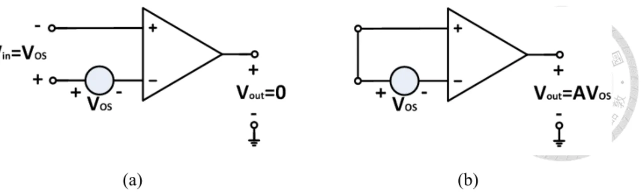
Because of the variation of the CMOS process, there are several non-ideal effects would limit the performance of the CMOS operational amplifier, such as offset and noise effect. Input offset in a system is generally defined as the input level that forces the output level to go to zero. For an amplifier, as shown in Fig 3.1.1-1 [3], the input offset is the differential input voltage that forces the output voltage to go to zero, typically in the range 100uV to 10mV. Due to the amplifier's high voltage gain, input offset voltage virtually assures that the amplifier output will go into saturation. This definitely reduces the performance of the CMOS operational amplifier.
(a) (b)
Fig. 3.1.1-1 Amplifiers with offset (a) differential input voltage equal to input offset voltage forces output to zero, (b) output offset of an amplifier with shorted input
3.1.2 Noise
Noise is an unwanted random addition to a signal. It limits the minimum signal level that a circuit can process with acceptable quality. Analog signals processed by integrated circuits are corrupted by interference noise (or man-made noise) and device electronic noise. The former refers to random disturbances that a circuit experiences through the supply or ground lines. The latter refers to thermal noise and flicker noise.
Fig. 3.1.2-1 shows the easy concept of the signal interferes by noise [13]. In general, we strive to maximize the signal to noise ratio in a system. Therefore, noise reduction has been an important topic due to the reduced supply voltage.
Fig. 3.1.2-1 Concept of signal interferes by noise
Chapter 3 Fundamentals of Analog Front-End
Fig. 3.1.2-2 Noise spectrum of standard CMOS amplifier
A conventional CMOS amplifier has a typical input-referred noise spectrum which as shown in Fig.3.1.2-2. For relative high frequencies, the noise, which spreads widely over the entire frequency band, can be considered as white noise. This is usually called the thermal noise floor. At low frequencies, the noise is increasing almost linearly with decreasing frequency and is generally called flicker noise. The frequency at which the noise becomes dominant over the white noise is called the noise corner frequency. At very low frequencies, offset becomes the dominant error.
Although offset is usually modeled as a time-invariant voltage source, it may change due to aging and temperature variations. This implies that it has a certain bandwidth and can be considered as a very low-frequency noise source.
3.1.2.1 Thermal noise [1]
Thermal noise is a wide spectrum of electromagnetic noise appearing in electronic circuits and devices as a result of the temperature-dependent random motions of electrons and other charge carriers.
Fig. 3.1.2.1-1 Representation of resistor thermal noise by a current source
As shown in Fig. 3.1.2.1-1, the thermal noise of a resistor R can be modeled by a parallel current source, with the spectral density:
or -(3.1)
Where k = 1.38×10⁻²³ J/K is the Boltzmann constant. Note that is expressed in
A2/Hz, is expressed in V2/Hz.
Fig. 3.1.2.1-2 Representation of MOSFET thermal noise by a current source
R In2 4kT
= Vn2 =4kTR
In2
n2
V
Chapter 3 Fundamentals of Analog Front-End
MOS transistors also exhibit thermal noise. The most significant source is the noise generated in the channel. For long-channel MOS devices operating in saturation, the channel noise can be modeled by a current source connected between the drain and source terminals. Fig. 3.1.2.1-2 shows the MOSFET thermal noise by a current source with the spectral density:
or -(3.2)
The coefficient γ is derived to be equal to 2/3 for long-channel transistors and may need to be replaced by a larger value for submicron MOSFET.
3.1.2.2 Flicker noise [1]
As charge carriers move at the interface between the gate oxide and the silicon substrate in a MOSFET, the trap-and-release energy states phenomenon associated with the dangling bonds would introduce flicker noise in the drain current. In electronic devices, it is a low-frequency phenomenon, as the higher frequencies are overshadowed by thermal noise from other sources. In MOSFET, flicker noise can be modeled as a voltage source in series with the gate and roughly given by:
-(3.3) In2 = 4kTγ gm
m
n g
V2 4kTγ
=
f WL C V K
OX n
2 1
⋅
=
Where K is a process-dependent constant on the order of 10-25 V2F. As this equation shows, flicker noise is proportional to 1/f, and therefore, flicker noise is also called 1/f noise.
The inverse dependence of (3.3) on WL suggests that to decrease 1/f noise the device area must be increased. Besides, PMOS devices exhibit less 1/f noise than NMOS devices because the former carry the holes in a buried channel.
3.2 Low-Offset and Low-noise Technique
Noise reduction has become increasingly important in modern technology with reduced supply voltage. Because the sensitivity of CMOS amplifiers is always limited by offset and noise, some techniques such as auto-zero technique or the chopper technique are presented to decrease them. The fundamental difference between them is offset handing. While the auto-zero principle is time-modulated, chopper technique is frequency-modulated.
Chapter 3 Fundamentals of Analog Front-End
3.2.1 Auto-zero technique
(a)
(b)
Fig. 3.2.1-1 Principle of Auto-zero technique (a) Phase 1, ϕ=1 (b) Phase 2, ϕ=0
The principle of auto-zero technique is depicted in Fig. 3.2.1-1 [15]. The offset cancellation is done in two phases. First, as shown in Fig. 3.2.1-1(a), when ϕ=1 (sampling phase), S1,2 is closed and S3 is open. The amplifier is configured in negative feedback structure, and the amplifier’s offset is stored on capacitor. The voltage over the auto-zero capacitor C can be expressed as:
Second, as shown in Fig. 3.2.1-1(b), during ϕ=0(signal phase), S1,2 is open and S3 is closed. The sampled offset is subtracted from the input signal and amplified. The output voltage can be expressed as:
-(3.5)
A channel charge of switch S2 will feed into the auto-zero capacitor. This effect is called charge injection. Therefore, the overall residual offset can be expressed as:
-(3.6)
Because input offset voltage can be divided by the voltage gain, the residual offset is then dominated by the charge injection. The influence of the charge injection caused by switch S2 on the residual offset can be reduced by increasing the size of the capacitor. In addition, the leakage of the capacitor C during the amplification phase can cause residual offset. These two effects cannot be divided by the voltage gain because the auto-zero capacitor is already at the input.
Besides the offset, the auto-zero technique can also minimize the flicker noise of the amplifier if the sampling frequency fs is chosen higher than the noise corner frequency fcorner, as shown in Fig. 3.2.1-2. However, auto-zero technique has the problem of noise-folded at the frequency lower than sampling frequency fs.
Intuitively, it can be assumed that when the amplifier depicted in Fig. 3.2.1-1 is auto-zeroed, the broadband noise of the amplifier is projected onto the capacitor C. At the end of the sampling phase the input offset and noise voltage are held on the
VC = A(Vin+ VOS− VC) = A(Vin+ VOS− A
A +1VOS) = A(Vin+ 1 A +1VOS)
Voffset,residual = 1
A +1VOS+qinj 3 C
Chapter 3 Fundamentals of Analog Front-End
capacitor, which means that all components of noise above the auto-zeroing frequency will fold back due to aliasing. Fig. 3.2.1-2 shows that the noise at frequency lower than fs is about a•Vn,th, which is slightly higher than thermal noise.
Fig. 3.2.1-2 Noise spectrum of auto-zero technique
3.2.2 Chopper technique
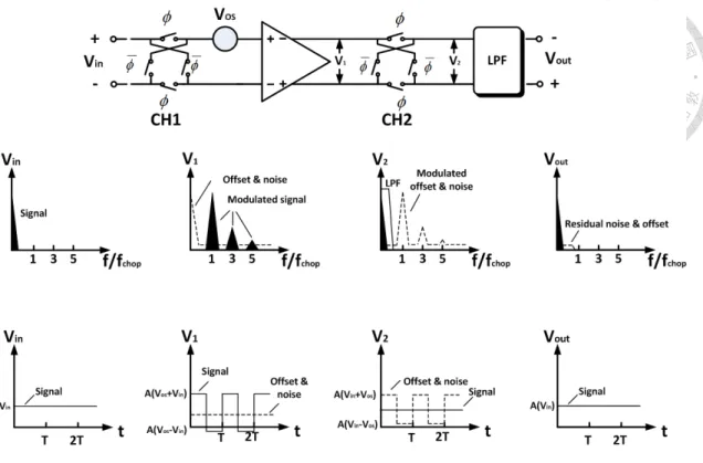
In chopper amplifiers the signal of interest and the offset signal are shifted to different frequencies. In Fig. 3.2.2-1, a chopper amplifier is shown [14]. This amplifier consists of a frequency modulator (or chopper CH1), a voltage amplifier, another chopper CH2, and a low-pass filter (LPF). The chopper switch is driven by a square wave φ with a chopping frequency fc.
Fig. 3.2.2-1 Principle of Chopper technique and its operation in Frequency/Time domain
From Fig. 3.2.2-1, we can know the method of operation of chopper technique both in frequency and time domain. The input signal is modulated to the chopping frequency at first. After amplify by an operational amplifier, the signal will be modulated back to the baseband. The offset and flicker noise is modulated only once and appears at the chopping frequency and its odd harmonics. At last, these frequency components can be removed through a low-pass filter.
The effect of chopper modulation can be analyzed from Fig. 3.2.2-2. Where Vin
is the input signal and m(t) is the carrier signal taking values of +1 and -1 with frequency of chopping frequency fc. It can be realized by two pairs of switch and complementary square wave φ and φ .
Chapter 3 Fundamentals of Analog Front-End
Fig. 3.2.2-2 Chopper modulation
The input signal Vin is multiplied by the square wave modulation signal m(t).
After this modulation, the output signal Vout is transposed around the odd harmonic frequencies of the modulation signal and is given by the following Fourier series:
-(3.5)
with -(3.6)
Therefore,
-(3.7)
According to (3.7), we can note that chopper modulation will shift offset and noise to the odd harmonic frequencies.
When a low-pass filter is used after the chopper amplifier, the chopper ripple and low-frequency noise can be filtered. CMOS amplifiers usually have a high DC input offset voltage and flicker noise. To reduce the flicker noise, the chopper frequency
∑
∞
= ⎭⎬⎫
⎩⎨
⎧ +
+
=
1 0
sin2 cos2
) (
n
n n
in t
b T T t a
a t
V π π
T T t
t T V
t t
Vin = < < in = < <
,2 0 ) ( 2 and 0
, 1 ) (
n nwt t
V
n
in 4 1sin
) (
...
5 , 3 , 1
∑
∞=
=π
From Fig. 3.2.2-1, this analysis can be concluded that the chopper technique completely reduces the 1/f noise when the chopper frequency is higher than the corner frequency of the 1/f noise. In practice the noise level of a chopper amplifier is slightly higher than the thermal noise level. Fig. 3.2.2-3 shows the noise spectrum of chopper technique. In contrast to the auto-zero technique, we can observe that the baseband noise of chopper amplifier is almost equal to the wideband thermal noise. Thus chopper technique is adopted to suppress the dc offset and low frequency in this thesis.
Fig. 3.2.2-3 Noise spectrum of auto-chopper technique
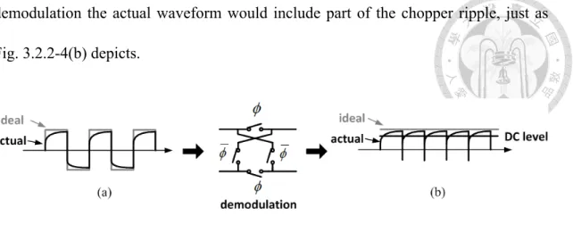
Although chopper technique has better performance on noise suppression than auto-zero technique, it still has some non-ideal effect. The ideal and non-ideal waveforms are depicted in time domain in Fig. 3.2.2-4. The gray line shows the ideal waveform and the black line shows the actual waveform. The limited bandwidth of the amplifier is a fundamental cause of switching glitches, so the square wave at the output of amplifier would not be like a perfect square wave. Therefore after
Chapter 3 Fundamentals of Analog Front-End
demodulation the actual waveform would include part of the chopper ripple, just as Fig. 3.2.2-4(b) depicts.
Fig. 3.2.2-4 Ideal and non-ideal waveforms of chopper amplifier in time domain (a) Amplifier output (b) Demodulated amplifier output
Another non-ideal effect is the residual offset caused by charge injection, which is generated by chopper modulator. Fig. 3.2.2-5 shows the basic concept of charge injection.
Fig. 3.2.2-5 Basic concept of charge injection
The gate voltage changes from high to low, transitioning the switch from closed to open state. When the gate of the NMOS transistor is high and the transistor is on, the voltage on the voltage source is sampled on the capacitor. When the gate of the NMOS transistor is low and the transistor is off, the voltage on the capacitor should
from the MOS switch create an error in the sampled voltage. When the transistor turns off, channel charge is dispersed into the source and drain so that charge injection occurs. This effect will cause channel charge entering the source or drain and introduces an error voltage.
Fig. 3.2.2-6 Charge injection model of a chopper modulator
Fig. 3.2.2-7 Residual offset caused by spike (a) Spike signal (b) Demodulation signal (c) Demodulated spike
Chapter 3 Fundamentals of Analog Front-End
Fig.3.2.2-6 is the charge injection model of a chopper modulator, where RS is the input resistor. C1 and C2 are the parasitic capacitors [33]. The effect of the mismatch between C1and C2 will be analyzed. When both lines are loaded with identical capacitors, no residual offset will occur since it will be a common-mode spike.
However, if there is a slight mismatch between the two capacitors, a differential component will also appear at Vout, which will translate into a residual offset, because these spikes are actually demodulated by the input chopper towards the input.
This effect is illustrated in Fig. 3.2.2-7 [33]. Therefore, each time the chopper clock switches charge is being injected into the input, this differential charge can be expressed by:
qinj=(C1-C2)Vspike-(3.8)
Where Vspike is the spike voltage generated by chopper modulator. This charge is applied two times the per clock period. This means that a current will run through the resistor RS. So the residual offset can be expressed by:
VOS=2(RS)(C1-C2)Vspikefc -(3.9)
Where fc is the chopping frequency. Since the time constant of these parasitic spikes is generally much smaller than the half chopper period, most of the spike appears at frequencies higher than chopper frequencies [3].
Transmission gate can reduces charge injection effect. As Fig. 3.2.2-8 depict, since the charge carriers in the NMOS and PMOS have inversed polarity. The
Fig. 3.2.2-8 Reduce charge injection effect by using transmission gate
3.3 Sub-threshold conduction design
Sub-threshold conduction is the current flows between the source and drain of a MOSFET when the transistor is operating in weak inversion region, that is, for gate-to source voltage VGS is below the threshold voltage Vth. Traditionally, we assumed that the device turns off immediately when VGS < Vth. In fact, for VGS ≈ Vth, a weak inversion layer still exists and some current flow between source and drain. Different from the current function when MOS is operating in saturation region, which is formulated as:
ID =1 2µCox
W
L
(
VGS−Vth)
2-(3.10)Sub-threshold conduction can be formulated as:
ID= I0⋅ e
VGS
nVT, VT =kT
q -(3.11)
Chapter 3 Fundamentals of Analog Front-End
Where n is a non-ideal factor, which is given by the capacitor divider:
n =Cjs+ Cox
Cox = 1+Cjs
Cox -(3.12)
Where Cjs is the depletion layer capacitance. Typically, n ≈ 1.5~2. To obtain the gm
factor from two modes, we have differentiation to ID and can get two separate equations:
Saturation region:
gm = dID
dVGS =µCOXW
L (VGS−Vth) = 2ID
VGS−Vth -(3.13) Sub-threshold region:
gm= dID dVGS =I0e
VGS
nVT
nVT = ID
nVT -(3.14)
To compare the pros and cons between these two regions, we introduce gm/ID
factor, which is also known as transconductance efficiency factor. It means we want a large gm, for as little current as possible. Therefore, (3.13) and (3.14) can turn into:
Saturation region:
OV th GS D m
V V V I
g 2 2
− =
= -(3.15)
Sub-threshold region:
gm ID = 1
nVT -(3.16) We can plot these two equations in Fig. 3.3-1.
Fig. 3.3-1 gm/ID plot
In Fig. 3.3-1, we can see that VOV
2 is fairly close for VOV > 150mV [13].
However, gm/ID does not approach to infinity for VOV → 0. It is obviously to observe that MOS operates in sub-threshold region has better transconductance efficiency than operates in saturation region. It means that we can get a larger gm value at same current condition when MOS operates in sub-threshold region. We can also observe that gm/ID is nearly a constant in sub-threshold conduction, which is similar to the behavior of BJT. Compare with the transconductance efficiency of BJT, it seems that we cannot do better than BJT even though the MOS is operating in sub-threshold region because it has a non-ideal factor n in its current function. The gm/ID value of sub-threshold conduction is about 1.5 times lower than BJT. However, in MOSFET
Chapter 3 Fundamentals of Analog Front-End
application, it is a great choice to have better transconductance efficiency by using sub-threshold conduction technique.
Besides to obtain the benefit of better tansconductance efficiency value, we can also analyze the noise effect when MOS operates in sub-threshold region. From equation (3.2), we already know that thermal noise spectral density of MOSFET is . If gm is as large as possible, the noise spectral density can be reduced to
a small value. Hence we can not only increase transconductance efficiency but also reduce the thermal noise spectral density by using sub-threshold conduction design.
3.4 Instrumentation Amplifier [33]
Fig. 3.4-1 Differential amplifier with resistive feedback
Bio-signal is a weak differential signal, which is often accompanies with a strong
m
n g
V2 4kTγ
=