國 立 交 通 大 學
電子工程學系 電子研究所碩士班
碩 士 論 文
混合訊號積體電路製程單晶片加速度計與
前端電路設計
Monolithic Accelerometer and Front-End Circuit
Design with Standard 0.18m Mixed-Signal
MEMS Process
研 究 生:王俊凱 Chun-Kai Wang
指導教授:溫瓌岸 博士 Dr. Kuei-Ann Wen
混合訊號積體電路製程單晶片加速度計與前
端電路設計
Monolithic Accelerometer and Front-End Circuit Design
with Standard 0.18m Mixed-Signal MEMS Process
研 究 生:王俊凱
Student:Hao-Ming Chao
指導教授:溫瓌岸 博士
Advisor:Dr. Kuei-Ann Wen
國立交通大學
電子工程學系 電子研究所碩士班
碩士論文
A Thesis
Submitted to the Department of Electronics Engineering & Institute of Electronics
College of Electrical Engineering and Computer Science
National Chiao Tung University
in Partial Fulfillment of the Requirements
for the Degree of Master of Science
in Electronic Engineering
July, 2011
HsinChu, Taiwan, Republic of China
I
混合訊號積體電路製程單晶片加速度計與
前端電路設計
學生:王俊凱 指導教授:溫瓌岸 博士
國立交通大學
電子工程學系 電子研究所碩士班
摘要
本文提出一個單晶片 CMOS MEMS 電容式加速度計與微瓦特前端電路。為了優 化加速度計的雜訊-功耗性能以達最小範圍,本文採用了一個目標規格驅動之電 路-微機電系統協同設計流程。這個共同電路-MEMS 設計流程,包括 CMOS MEMS 加速度計的質量-彈簧-阻尼參數計算流程和優化功耗-雜訊的讀出電路。在模擬 讀出電路設計中,本文提出的電路架構結合捷波穩定和相關雙重採樣的方式,用 以抑制低頻雜訊和直流偏移補償。在 RMS 輸入參考雜訊電壓在 100Hz 頻率下為 9.82 nV/√Hz,其功耗在 100 kHz 調波頻率下為 41W。 CMOSMEMS 加速度計的 設計流程說明了如何透過計算質量-彈簧-阻尼參數來得到最小化加速度計面 積。II
Monolithic Accelerometer and Front-End
Circuit Design with Standard 0.18m
Mixed-Signal MEMS Process
Student: Chun-Kai Wang Advisor: Dr. Kuei-Ann Wen
Department of Electronics Engineering
Institute of Electronics
National Chiao-Tung University
Abstract
A monolithic implemented with standard 0.18m Mixed-Signal MEMS (MS MEMS) process capacitive accelerometer with micropower analog front-end circuit is presented in this thesis. In order to optimize noise-power performance of the accelerometer, a specification driven circuit-MEMS co-design flow is adopted. The concurrent circuit-MEMS design flow includes mass-spring-damping parameter calculation flow for MEMS accelerometers and optimized power-noise reduction flow for readout circuits. In analog readout circuit design, the proposed circuit architecture combines chopper stabilization and correlated double sampling to suppress low frequency noise and compensate DC offset. The RMS input referred noise voltage is 9.82 nV/√Hz under 100Hz. The power consumption is 41W at 100 kHz modulation frequency. The integrated circuit and accelerometer design flow shows how to calculate mass-spring-damping parameter for minimized accelerometer area.
III
誌謝
很高興能夠完成這份碩士論文,將自己的研究成果做一個呈現,在兩年的時光 裡,能完成一份論文,對自己而言算蠻不容易的吧。 首先,要感謝的是指導教授 溫瓌岸老師的引導與督促,並且提供了豐富的學 習資源與優良的研究環境,使我在研究上的軟硬體方面能有充分的輔助,能順利 的設計加速度計與電路,並能完整的規劃研究行程,能在有限的時間內,順利的 達成目標。 接著,要感謝實驗室哲生學長、美芬學姐、文安學長、皓名學長。哲生學長對 於研究方向的指導,電路模擬規格方法的指點,與會議論文撰寫的修訂與建議, 與其他諸多幫助下,讓我能從模糊的目標,一步步的邁向完整的加速度計與電路 設計。美芬學姐對基礎研究搜索、閱讀方法與閱讀的深廣度的指導,使我能在研 究學習上夠能掌握重點。同時也感謝文安學長與皓名學長所提出的各項建議,使 我在設計時能有更全面的思考。 感謝實驗室的各位助理:宛君、智伶、淑怡、秀榕、幸玲,在行政上面給予相 當多的幫助,在眾多瑣事上能提供相當實質上的協助,特別是宛君與智伶在費用 上的協助。 也謝謝實驗室學長謙若、煜翔、崇閔、柏亨、哲誠;同學建原、峻澤;學弟昱 賢、竣傑、易達、柏翰、志峻,與我在實驗室一同打拼,昱賢學弟對於軟體的大 力協助是不可或缺的,與大夥在實驗的室生活充滿著研究生的回憶。 最後,要感謝的是我的父母親與妹妹,能支持我求學的決定,在家庭的後盾下 完成我的學業。 王俊凱 2011 年 7 月IV
Contents
摘要………..I
Abstract……….II
誌謝………...III
Contents………...IV
List of Figures………..VI
List of Tables………VIII
CHAPTER 1 INTRODUCTION ... 1 1.1 MOTIVATION ... 11.2 ORGANIZATION OF THE THESIS ... 4
CHAPTER 2 ARCHITECTURE ... 5
2.1 SYSTEM ARCHITECTURE AND SPECIFICATION... 5
2.2 SYSTEM DESIGN FLOW ... 6
CHAPTER 3 CMOS MEMS ACCELEROMETERS ... 8
3.1 CMOSMEMSACCELEROMETER FABRICATION ... 8
3.1.1 Surface Micromachining... 8
3.1.2 CMOS MEMS Design Rules ... 10
3.2 CMOSMEMSACCELEROMETER DESIGN ... 13
3.2.1 CMOS MEMS Structure ... 13
3.2.2 Accelerometer Layout Design Flow ... 20
V
4.1 FRONT-END CIRCUIT ARCHITECTURE ... 24
4.2 FIRST STAGE CIRCUIT DESIGN ... 25
4.2.1 First Stage Amplifier ... 25
4.2.2 Electronic Noise Analysis and Design Flow ... 27
4.3 CHOPPER STABILIZATION ... 30
4.4 CORRELATED DOUBLE SAMPLING ... 31
4.5 SECOND STAGE CIRCUIT DESIGN ... 33
CHAPTER 5 IMPLEMENTATION ... 35
5.1 SIMULATION ... 35
5.1.1 CMOS MEMS Accelerometer Simulation ... 35
5.1.2 System Simulation... 37
5.1.3 Input referred Noise Simulation ... 42
5.1.4 Capacitive Sensing Mismatch Simulation... 43
5.1.5 Figure of Merit Comparison ... 44
5.2 MEASUREMENT RESULTS ... 45 CHAPTER 6 CONCLUSIONS ... 52 6.1 SUMMARY ... 52 6.2 FUTURE WORK ... 52 BIBLIOGRAPH ... 55 VITA ... 57
VI
List of Figures
Figure 2.1: Architecture diagram of the accelerometer with readout circuit. ………...5
Figure 2.2: Design flow chart of the system. ………7
Figure 3.1: Post-CMOS micromachining steps: (a) after completion of CMOS, (b) anisotropic oxide etch, and (c) isotropic silicon etch to release the microstructures. ………...9
Figure 3.2: Rule definitions. ………..……..11
Figure 3.3: Examples of the RLS-mask definition. ……….13
Figure 3.4: (a) Schematic of accelerometer and (b) lumped parameter model of accelerometer. ………...14
Figure 3.5: Multi-turn folded-beam spring. ………16
Figure 3.6: Capacitive sensing by a capacitive divider. ………..16
Figure 3.7: Fully differential capacitive sensor. ………..18
Figure 3.8: Accelerometer design flow chart. ……….18
Figure 3.9: Single axial accelerometer dimension parameter for core area. ……..….21
Figure 3.10: Single axial lateral accelerometer layout design flow. ………...22
Figure 3.11: The accelerometer area versus the spring number. ……….22
Figure 3.12: Dual axial lateral accelerometer dimension parameter for core area. ….23 Figure 4.1: Front-end circuit architecture. ………..24
Figure 4.2: Schematic of the non-overlapping two phase clock generator and its timing diagram. ………25
Figure 4.3: The schematic of the first stage amplifier. ………26
Figure 4.4: Circuit noise model of the capacitive-sensing frond-end. ………27
VII
Figure 4.6: Electronic power-noise design flow. ………29
Figure 4.7: Chopper stabilization technology principle. ……….31
Figure 4.8: Schematic of correlated double sampling. ………32
Figure 4.9: The schematic of the second stage amplifier. ………...33
Figure 5.1: Finite element model of the one axial accelerometer. ………..35
Figure 5.2: Resonant frequency model of the one axial accelerometer. ……….36
Figure 5.3: Equivalent model circuit of the accelerometer. ………37
Figure 5.4: Simulated output square noise power. ………..42
Figure 5.5: Layout of the accelerometer with front-end circuit chip. ……….45
Figure 5.6: Die photo of the accelerometer chip. ………46
Figure 5.7: Photo of the test setup. ………..47
Figure 5.8: Waveform of (a) reference accelerometer and (b) test chip with a 100-Hz 1-g acceleration input signal. ………48
Figure 5.9: Output spectrum of (a) reference accelerometer and (b) the test chip with a 100-Hz 1-g acceleration input signal. ...………49
Figure 5.10 Output spectrum of the test chip. ……….50
Figure 6.1: The roadmap of miniaturization of the digital functions ("More Moore") and functional diversification ("More-than-Moore"). ………..53
VIII
List of Tables
Table 2.1: System Specification……….6
Table 3.1: RLS design rule definitions in CMOS MEMS Process………..12
Table 5.1: Calculation versus simulation data………..36
Table 5.2: Mechanical parameter transfer to electronic parameter………..38
Table 5.3: Pre-simulation of all corner status………...39
Table 5.4: Post-simulation of all corner status……….39
Table 5.5: Pre-simulation under voltage variation………...40
Table 5.6: Post-simulation under voltage variation………..40
Table 5.7: Pre-simulation under temperature variation………41
Table 5.8: Post-simulation under temperature variation………..41
Table 5.9: Simulation under sensing mismatch………...43
Table 5.10: Performance comparison………...44
Table 5.11: Equipment/instrument used in experiments………..47
1
Chapter 1
Introduction
Over the past decade, micro fabrication technology have enabled the integration of sensors and actuators with microelectronic circuits, called MicorElectroMechanical System (MEMS). Furthermore, integration of micro-machining structure and readout circuits into single chip has been developed growly due to its economic value. Monolithic CMOS (complementary metal-oxide-semiconductor) MEMS sensors with different kind of circuits will be applied to wide range of applications. This thesis presents a methodology for CMOS MEMS accelerometer design: concurrent circuit-MEMS design flow which includes mass-spring-damping parameter calculation flow for CMOS MEMS accelerometers and optimized power-noise reduction flow for readout circuits. The concurrent circuit-MEMS design flow can be used to co-design the system of accelerometers and analog front-end circuits. Mass-spring-damping parameter calculation flow provides a methodology for CMOS MEMS accelerometer design. Optimized power-noise reduction flow includes the power-noise design flow and noise reduction methodology for micro-power low noise readout circuit design.
1.1 Motivation
MicroElecroMechanical Systems (MEMS) is the technology of very small mechanical devices driven by electricity. The MEMS technology offers the capability
2
to manufacture integrated system of complex functionality on a single substrate at low cost and high volume. MEMS sensors and actuators, which are devices that convert a non-electrical quantity into an electrical signal and vice versa, involve additional quantities that can be sensed, such as acceleration, angular velocity, and pressure.
One of the most important silicon-based sensors is micro-machined inertial sensor, comprising accelerometers and gyroscopes[1]. Accelerometers can be used to detect the magnitude and direction of the acceleration, i.e., to sense orientation, vibration and shocks. Since 1990s, MEMS accelerometers have been used extensively in airbags as crash sensors, and since then motion sensors have been widely introduced to different systems including smart handhelds.
The integration of the standard CMOS process and various CMOS post-processes for MEMS applications have been summarized in [2].Microstructures may be formed using either pre-CMOS, intra-CMOS and post-CMOS fabrication approaches. In general, the CMOS post-processes to fabricate suspended MEMS structures can be integrated into standard CMOS process significantly. So that CMOS MEMS processes have the advantage of monolithic integration of the integrated circuit (IC) and micromechanical components[3].
CMOS MEMS accelerometers are applied for a wide range of applications, including automotive safety, virtual reality, movement detection, various navigation system, and mobile devices. A CMOS MEMS accelerometer has the advantages of low temperature coefficient, low power dissipation, low noise, and low cost due to its compatibility with wafer fabrication process. However, monolithic CMOS MEMS accelerometers fabricated with standard ASIC process can have relatively smaller sensing capacitance, of which the differential relative variation usually on the order of
3
10-16 ~10-15F within the bandwidth ranging from several Hz to several hundred Hz, and that cause low mechanical sensitivity [4-6]. Therefore, the main design consideration is how to suppress low frequency noise and DC offset in readout circuit design. Furthermore, for wireless devices and portable consumer electronics devices, the power dissipation is another critical design consideration for the capacitive sensing sensors. Hence, low power design becomes another issue for wireless applications.
One of the readout circuits widely used in CMOS MEMS accelerometers is switched-capacitor (SC) charge integration method [7-9]. The correlated double sampling (CDS) technique has been used to significantly reduce the DC offset and low frequency noise. The main drawback of the SC circuit is the related high kT/C noise with small feedback capacitor. The other one of the readout circuits is continuous-time voltage (CTV) method [10-12]. The chopper stabilization (CS) technique is employed to reduce the DC offset and low frequency noise. Both of the two noise reduction techniques could be integrated into one capacitive sensing readout circuit [13-15]. However, the low noise readout circuits consume a power of few mW, and the low power readout interface circuits generate a noise of a few hundred μg/√Hz.
In this work, both the readout circuit and a CMOS MEMS accelerometer are implemented. In accelerometer with readout circuit design, a specification driven MEMS/IC co-design flow is proposed. Low noise and compact accelerometer could be achieved. The proposed readout circuit combines the chopper stabilization technique and the correlated double sampling to reduce low frequency noise and DC offset. Our approach is to design an accelerometer with front-end circuit system.
4
1.2 Organization of the Thesis
This thesis presents the design of accelerometer with readout circuits, including design flow chart, single-axial accelerometer design, and a micro-power low noise readout circuit. Chapter 2 describes the system specification and the design flow. In chapter 3, a single-axial accelerometer design would be presented. We are going to show what the fabrication flow is, and introduce the accelerometer area design flow under the process constraint. In chapter 4, the front-end circuit with chopper stabilization and correlated double sampling technology is described from architectural level down to detail design. The simulation and measurement results are presented in chapter 5. Chapter 6 concludes dissertation with summary, and suggestion for the future work.
5
Chapter 2
Architecture
2.1 System Architecture and Specification
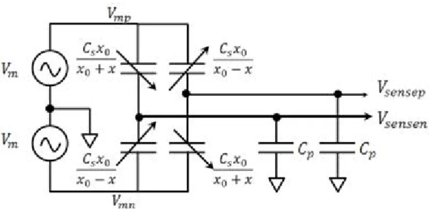
The architecture of the accelerometer with readout circuit is shown in Fig. 2.1, where the fully differential capacitive bridge represents the sensing capacitors of the accelerometer. A1 is the first stage amplifier, A2 is the second stage amplifier, and
clocking is used for chopper stabilization and correlated double sampling technology. The design goal is to achieve 12-bit resolution under 1.2V peak to peak output swing with ±4g input sensing range. The bandwidth of the CMOS MEMS accelerometer is up to 100Hz. Design target for the output noise voltage should be less than half the LSB, i.e. 14.6μV/√Hz for 100Hz bandwidth. The sensitivity could be 150mV/g due to
6
1.2Vpp with ±4g sensing range. Assume the voltage swing at sensor output is 1mV/g,
the voltage gain readout circuit can be obtained as 44 dB.
Considering noise and linearity, the voltage gain of the second stage amplifier is set to be 22dB. The gain of the first stage amplifier with the CDS circuit is 22dB. The input-referred noise is 97.3nV/√Hz. Because low noise circuit design is more easily to be achieved than MEMS design, the noise constraint of readout circuit is set to be one fourth of total noise.
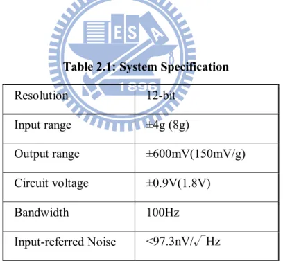
The system specification is shown in table 2.1. In order to achieve 12-bit resolution, the noise constraint is the critical design consideration. The noise comes from the mechanical noise of the accelerometer and the electronic noise of the readout circuit.
Table 2.1: System Specification
Resolution 12-bit Input range ±4g (8g) Output range ±600mV(150mV/g) Circuit voltage ±0.9V(1.8V) Bandwidth 100Hz Input-referred Noise <97.3nV/√Hz
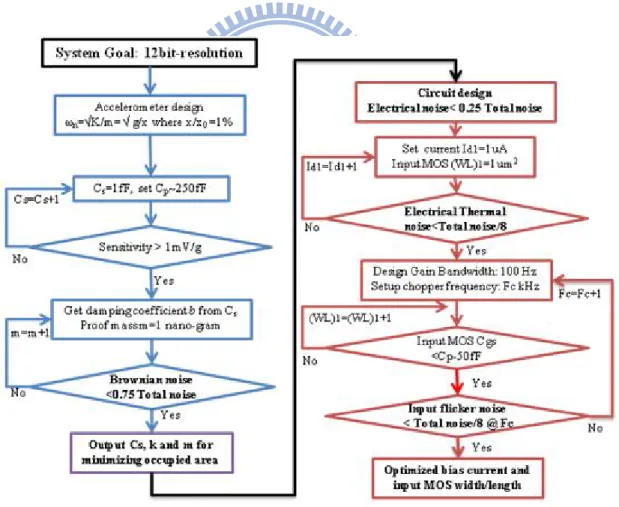
2.2 System Design Flow
A specification-driven accelerometer design flow is proposed in this thesis. The target of this design flow shown in Fig. 2.2 is to achieve 12-bit resolution. To get the
7
minimum occupied area of accelerometer under required system performance for sensor and to get the optimized bias current and width of the input MOS for analog front-end. The left part belongs to the accelerometer design flow. The noise constraint comes from the Brownian noise, and is set to be less than 75% the total noise.
The accelerometer could be divided into three parts: spring, sensing fingers and proof mass. In order to minimize the area of the accelerometer, the correlation between geometry parameters and mechanical properties should be found first. The circuit design is to get the optimized bias current and MOS width/length of the input transistors under the noise constraint. The detailed design considerations will be described in the follow sections.
8
Chapter 3
CMOS MEMS Accelerometers
3.1 CMOS MEMS Accelerometer Fabrication
3.1.1 Surface Micromachining
The accelerometer described in this thesis is designed with the 0.18μm CIC (National Chip Implementation Center) CMOS MEMS technology. The process starts with TSMC 0.18μm mixed-signal/RF CMOS process. The process flow is shown in Fig. 3.1(a) incorporates the TSMC 0.18μm 1poly-6metal CMOS process. The micromachining process is performed on the wafer after the standard CMOS process. The passivation above the microstructure will be removed during CMOS process. And the passivation layer above the electronic circuits is preserved to protect the devices during the MEMS process. In Fig. 3.1(b), after the CMOS processing, an anisotropic reactive ion etch (RIE) is the first performed to etch away SiO2 that is not
covered by photoresist, resulting in vertical sidewalls. At the final step, the isotropic dry etching shown in Fig. 3.1(c) is used to etch the silicon substrate and release the microstructures.
CIC CMOS MEMS technology requires an additional lithography step, which is different from the process in [4]. The post-process flow is completed by two simple dry etch steps.
9
(a)
(b)
(c)
Figure 3.1: Post-CMOS micromachining steps: (a) after completion of CMOS, (b) anisotropic oxide etch, and (c) isotropic silicon etch to release the microstructures.
10
Main advantage of this process is that it offers the integration of MEMS and electronics, therefore allows on-chip signal detection, signal processing and control to be implemented. Complex system-on-chips (SOC) can be fabricated at low cost. The integration enhances the performance and functionality of MEMS systems, and reduces the system cost.
However, the structure of CMOS MEMS technology severely limits the device performance. The microstructures have small mass in the order of 10-9 kg, resulting in low sensitivity to outside force, and several orders of magnitude higher Brownian noise than bulk micromachined devices. In the 10 m thick structures, the devices have low capacitance for sensing. The total capacitance of the designed device is about 100 fF. This leads to the low sensor sensitivity. And the situation of the low sensitivity is further aggravated by the structural curling of the composite surface post -process structures. The multi-layer structural material, composed of metal layers with interleaved dielectric layers, exhibits residual stress gradients that induce structural curling [5]. The different curvatures in different parts of the devices cause mismatches between electrodes, which further reduces the capacitance and capacitance sensitivity. Also, the CMOS MEMS structures exhibit large lateral mismatch which causes large variable position offset in differential sensing devices.
3.1.2 CMOS MEMS Design Rules
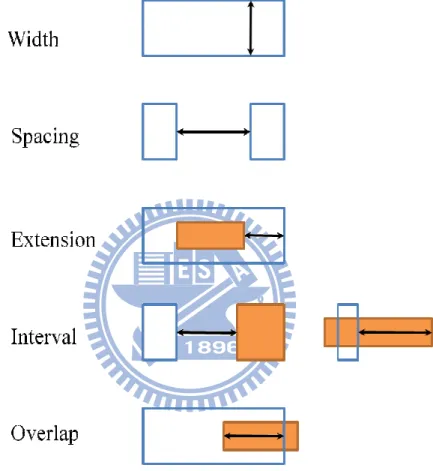
In the process, the design rules are defined by TSMC. All design rules defined in this section are applied to construct the structure of microelectromechanical devices. To achieve the post process successfully, all design rule errors are not allowed. Design rule definitions are shown in Fig. 3.2. These definitions are used for the distance constraint of multiple layers. In CMOS process, the passivation (PAD) mask
11
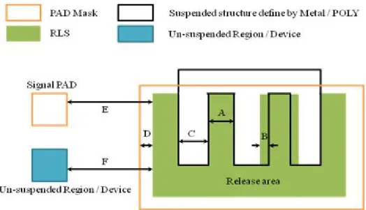
defines the removal of silicon-nitride and gives an open-window on the signal pad. To guarantee the oxide etching process in CIC post-process, PAD mask is also necessary to overlap the RLS region, which defines the MEMS etching region. Besides, PAD mask can also help pass some DRC rules on large metal area.
Figure 3.2: Rule definitions.
RLS mask defines the MEMS etching region in post-process, and the design is shown in Table 3.1 and Fig. 3.3. Note that if the expected structural line width or spacing is beyond the limit of lithography (< 4 m) in post process, metal layer can be used as the hard-mask for the purpose of high resolution, but it is not guaranteed to be successful. Using metal layer as the hard-mask may cause polymer around the border, especially when the exposed metal area is large, so the metal layer overlapped with
12
the RLS mask must be restricted to 1m and the yield rate of spacing < 4 m is much lower than which of the spacing > 4 m.
Table 3.1: RLS design rule definitions in CMOS MEMS Process
Rule # Description Rule (m) RLS.W.1 Min. width of RLS A 4m
RLS.METALx.1 Max. overlap of RLS on Metal (If using Metal as hard mask)
B 1m
RLS.Poly.1 Max. overlap of RLS on POLY B 1m
RLS.S.1 Min. spacing between RLS regions C 4m
RLS.PASS.1 Min. /Max. extension of PAD mask over RLS mask
D 1m
RLS.PASS.2 Min. interval between wide RLS (width > 20m) and SINGAL PAD
E 50m
RLS.ACTIVE.1 Min. interval from RLS to unsuspended PMOS or NMOS
F 50 m
RLS.Cap.1 Min. interval between wide RLS (width > 20m) and un-suspended capacitors
F 50 m
RLS.Res.1 Min. interval between wide RLS (width > 20m) and un-suspended resistors
F 50 m
RLS.R.1 Max. area ratio of RLS to wide RLD (width > 100 m) in etching region
60%
Since silicon substrate under the RLS region will be etched in post-process, electronic circuits are forbidden in RLS regions.
13
Figure 3.3: Examples of the RLS-mask definition.
3.2 CMOS MEMS Accelerometer Design
3.2.1 CMOS MEMS Structure
The geometry of single axial accelerometer and simplified lumped model is shown as Fig. 3.4. The springs, sensing fingers and proof mass build the core structure of the accelerometer. The anchors are used for connecting the sensor structure.
An accelerometer is a force sensor. The external acceleration generates an inertial force on the proof-mass. The inertial force then induces the displacement of the proof mass. With the operation range of the accelerometer, both the spring elastic force and the viscous damping force are linear with the displacement and the velocity of the proof-mass, respectively. The differential equation of displacement and external acceleration of sensor is given:
14
where m is the mass of proof mass, b is the damping coefficient x is the displacement, and k is the stiffness of spring.
(a)
(b)
Figure 3.4: (a) Schematic of accelerometer and (b) lumped parameter model of accelerometer
With the 1st order approximation, the equation of displacement can be simplified as:
=
(3-2)15
=
(3-3)At frequencies much lower than the resonant frequency, the sensitivity of the accelerometer is given by:
=
=
(3-4)Based on Eq. 3-4, the resonant frequency of sensor can be defined by the maximum displacement at maximum sensing gravity. For this design consideration, with 4μm comb finger gap process constraint, we set up 1% displacement of the gap under 1g external accelerometer. Because the larger displacement elevates the nonlinearity but the less displacement makes the initial offset voltage of the sensor structure mismatch worse. The resonant frequency is 2.5kHz through the settings.
Figure 3.5 shows the folded-beam spring used in the accelerometer. The spring constant in the x-axis is given by:
=
ℎ
(3-5)where Nk is the number of turns, E is the Young’s modulus of elasticity, and lk, wk, h
are the length, width and height(thickness) of the beam respectively. In the accelerometer design, the beam width is 4 μm, and the beam height is the thickness of the composite structure, which is about 10 μm.
In CMOS MEMS accelerometers, capacitive sensing converts the mechanical displacement into electrical signal. When the proof mass moves in the sensing direction, the gap distances between the rotor and stator fingers change, and the capacitance of the parallel-plate capacitors changes accordingly. The capacitance
16
change induces a charge transfer in the capacitors, which generates an AC voltage or an AC current.
Figure 3.5: Multi-turn folded-beam spring.
A capacitive divider provides a voltage-domain description of the sensing process as shown in Fig.3.6. The capacitance of one sensing capacitor increases, while the capacitance of the other capacitor decreases when the proof-mass moves in one direction. Thus, a voltage proportional to the displacement is generated. The sensitivity is limited by the parasitic capacitance which includes the fringe capacitance, the interconnect capacitance, and the input capacitance of the interface circuit.
Figure 3.6: Capacitive sensing by a capacitive divider.
17
=
∙
=
∙
∙
(3-6)
where Cs is the sensing capacitance of sensor, Cp is the parasitic capacitance at sensor
output node, Vm is the voltage swing of modulation signal and x0 is the gap between
two fingers. The sensed voltage can be rewritten as a Taylor series as:
=
+
−
+ ⋯
(3-7)The existence of the parasitic capacitance gives rise to the nonlinear terms. When the displacement is sufficiently small, as in the case of accelerometers, the above equation can be approximated by a linear voltage-displacement relationship:
=
∙
∙
(3-8)As shown in Fig. 3.7, the CMOS MEMS accelerometer employs a differential capacitive bridge consisting of two differential dividers to realize fully differential sensing. The fully differential topology improves the inference rejection of the sensor with much high common-mode rejection ration (CMRR) and power supply rejection ration (PSRR). The sensed voltage in a differential sensor is as:
=
−
=
∙
∙
(3-9)
The sensed signal is an amplitude modulation (AM) signal with the acceleration signal modulated by a high frequency modulation carrier. The sensitivity of the accelerometer is proportional to the amplitude of the modulation carrier, Vm.
18
Figure 3.7: Fully differential capacitive sensor.
The accelerometer design flow is shown in Fig. 3.8. With 4μm comb finger gap process constraint, 1% displacement of the gap under 1g external accelerometer, the resonant frequency is about 2.5kHz, and the modulation voltage is 0.3V. The sensing capacitance Cs would be increased to achieve 1mV of the sensitivity of the
accelerometer.
19
The sensing capacitance Cs can be expressed as:
= (3-10)
N is the number of fingers, l is the finger length, x0 is the gap between fingers, air is
the dielectric constant of the air, and t is the thickness of each finger. From Eq. 3-9 and Eq. 3-10, the larger area of comb fingers, the higher voltage swing at sensor output node with fixed parasitic capacitor.
A direct consequence of air damping is the thermal-mechanical noise, a random force generated by the Brownian motion of ambient molecules. It is normally called Brownian noise. For accelerometers, the power spectral density (PSD) of the Brownian noise is:
( ) =
( . ) (g ⁄Hz) (3-11)
where kb is Boltzmann’s constant (1.38×10⁻²³ J/K), T is temperature, b is damping
factor and m is the weight in kg of proof mass. And the input-referred Brownian noise floor is:
( ) =
. (g √Hz⁄ ) (3-12)
There are two sources of mechanical damping: the structural damping; and the viscous damping by gas flows. The CMOS MEMS structures are made of Aluminum and SiO2, both are high-Q materials with very low structural damping. The damping
in CMOS MEMS devices is mainly caused by the viscous flow of gas surrounding the micro structures. The dominant damping mechanism in lateral accelerometer is
20
squeeze-film damping between lateral parallel-plate capacitor fingers. The squeeze- film damping can be modeled as:
= 7.2
(3-13)
μ (1.85×10⁻⁶ ∙ / ) is the viscosity of the air under atmospheric pressure at room temperatureFrom Eq. 3-10 and Eq. 3-13, we can find the damping factor is proportional to sensing capacitance with fixed thickness t, comb finger number N, finger length l, and gap x0.
With the damping factor being specified, the minimum proof mass will be calculated by Eq. 3-12. Then the spring constant will also be specified by Eq. 3-3. The sensing capacitance Cs, spring constant k, and proof mass m can be used for design
the accelerometer as the purpose of the accelerometer design flow.
3.2.2 Accelerometer Layout Design Flow
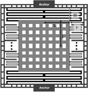
The accelerometer dimension parameter for core area is shown in Fig. 3.9. H is the total length of the spring turns, W is the half width of the proof mass, L is the half length of the proof mass, and F is the comb finger length plus the gap between finger and rigid frame. As described in section 3.1.2, the minimum width and minimum gap are both 4m according to the design rule. The sensing capacitance Cs, spring
constant k, and proof mass m which are gotten in previous section can be used for the area design.
The single axial accelerometer layout design flow is shown in Fig. 3.10. Based on the parameter sensing capacitance Cs, spring constant k, and proof mass m, the
21
comb finger length and number to fit the sensing capacitance value. The area of F×L would be minimized if the number of comb finger N is set to be 1, but the finger length/width ratio would be larger than 100. Due to the curvature issue [5], the length/width ratio of the comb finger should be less than the maximum value constrained by foundry rules. Without foundry data, we assume the ratio to be ρ for our tuning parameter. With width 4 m, the length of F would be calculated. The number of comb fingers would also be determined base on the capacitance data. Then the proof mass length 2L can be calculated from the comb finger number.
Figure 3.9: Single axial accelerometer dimension parameter for core area
From the value of the sensing capacitance and the length/width ratio of comb fingers, both F and L can be determined as shown in step two of the accelerometer layout design flow in Fig. 3.10. Then we choose the minimum turn of the spring to get the parameter H. In order to satisfy the minimum proof mass, the W can be increased.
22
Then W is increased to fit the design setting of resonant frequency from Eq. 3-5. The core area will be gotten from the parameters F, H, L, and W. We keep increasing the spring turn number to run the loop until outputting the minimum area as shown in Fig. 3.10.
Figure 3.10: Single axial lateral accelerometer layout design flow.
The comb finger length/width ratio is set to be 78m/4m that is less than 20 for curvature consideration. After calculation of the layout design flow, the figure of the accelerometer area versus the spring number is shown in Fig. 3.11. We could find out
Figure 3.11: The accelerometer area versus the spring number.
3.00E-07 3.10E-07 3.20E-07 3.30E-07 3.40E-07 3.50E-07 3.60E-07 3.70E-07 3.80E-07 3.90E-07 4.00E-07 0 1 2 3 4 5 6 7 A cc e le ro m e te e r a re a (m 2) Spring number
23
that the minimum area comes out when the spring number is 4.
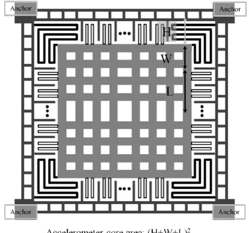
This method can also be used for dual axial lateral CMOS MEMS accelerometer design. It would be simpler than the design flow of single axial accelerometer. Because the layout of the accelerometer is symmetry, the less parameter makes the design flow easier. The accelerometer dimension parameter for core area is shown in Fig. 3.12. There are three parameters for layout dimension design. In this thesis, dual axial accelerometer will be discussed further due to single axial accelerometer is what we design for the system.
24
Chapter 4
Front-End Interfacing Circuit
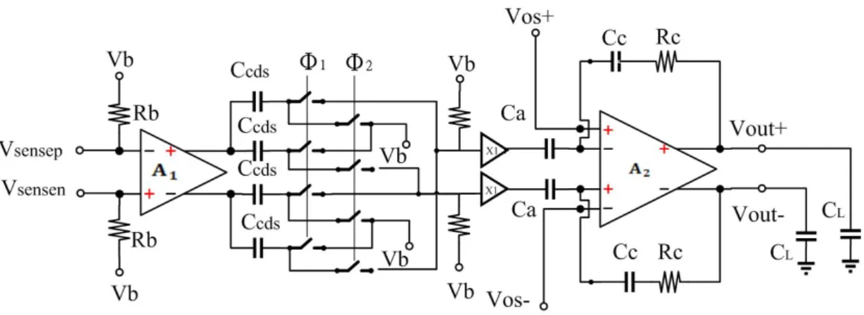
4.1 Front-end Circuit Architecture
The analog front-end circuit is shown in Fig 4.1. The fully differential topology is employed to reject CMRR and PSRR. The input resistors Rb are replaced by
diode-connected PMOS devices for providing DC bias at input nodes. There should be large impedance at input node, but using resistors would cost larger area. The diode-connected PMOS devices can also provide high impedance at input nodes and cost much smaller area than using resistors. But the tradeoff is that the diode-connected PMOS devices have capacitance and smaller bias current. Depending on 0.18μm CMOS technique, the capacitance of it is in the order of fF and the leakage current is about several nA. The value of capacitance and bias current could be tolerable to the circuit performance.
25
The first stage amplifier A1 design is to achieve reasonable gain boost, to optimize
power-noise performance, and to limit the operation bandwidth. Then a CDS technique is used to subtract out the output error voltage of the first stage amplifier with two sequential samplings. The following second stage amplifier is a closed loop amplifier. The amplifier is designed for satisfying the gain of the system requirement and is working as a low pass filter. The modulation signals are generated the logic gates as shown in Fig. 4.2. The non-overlapping two phase clocking is designed to avoid the overlapping of the two phase clocking. The clock overlapping will cause the charging error.
Figure 4.2: Schematic of the non-overlapping two phase clock generator and its timing diagram.
4.2 First Stage Circuit Design
4.2.1 First Stage Amplifier
The two-stage topology is preferred to the single-stage topology for the following reasons. First, the power-noise optimization requires the input transistors to adjust width/length ratio, therefore, they do not have sufficiently large transconductance to
26
drive the entire high-gain wide-band amplifier. Second, the two-stage topology makes it easy to implement offset compensation and minimizes the noise contributed by offset compensation circuits. Third, a low-gain input stage could achieve the following goals: minimizing main noise contributing devices; amplifying signal to attenuate noise from the following circuits; limiting gain to prevent large sensor position offset from saturating the circuit from the beginning; limiting gain to reduce Miller effect.
The schematic of the first stage amplifier is shown in Fig 4.3. The overall gain is 44dB. The CDS will double the output voltage so that its gain is 6dB. The first stage
Figure 4.3: The schematic of the first stage amplifier.
is an open-loop amplifier with a gain of about 16dB. The open-loop amplifier A1
architecture is believed to have better noise performance because it suffers less from noise folding compared with transimpedance amplifiers and capacitive feedback amplifiers [8]. Transistor m5 and m6 draw the DC current from the load branch to increase the impedance of the diode-connected load transistors to ensure proper gain. The input transistors m1, m2 and load transistors m3, m4 are of the same type, so the
27
temperature dependences of the input and load transistors will cancel each other out, making less sensitive to temperature variation.
4.2.2 Electronic Noise Analysis and Design Flow
Electronic noise comes from the following sources as shown in Fig. 4.4: the thermal noise of the input transistor, the flicker noise of the input transistor, the bias noise due to bias current of the diode in the biasing circuit, the noise from the modulation signal, and the noise from the following stages and the load of the circuit. The residue noises from the voltage references and the corresponding switches for generating the modulation signals may be injected into the sensing node, and the bias noise is negligible with small bias current. The noise contributions by the loads and the following stages can be neglected by dividing the first stage gain. The total noise will be dominated by the input transistors. Both thermal noise and flicker noise of the input noise are the critical issue for design consideration.
Figure 4.4: Circuit noise model of the capacitive-sensing frond-end.
A conventional CMOS amplifier has a typical input-referred noise spectrum, as shown in Fig. 4.5. For rather high frequencies, the noise can be considered as
28
frequency independent or white. This is called the thermal noise floor. At low frequencies, the noise power increases almost linearly with decreasing frequency and is therefore commonly called flicker noise. The frequency at which the flicker \noise becomes dominant over the white noise is called the flicker noise corner frequency fknee.
Figure 4.5: Noise power spectrum of standard CMOS amplifier.
The mean square equivalent input noise could be expressed as below:
= + ≅ 2 4 1 + ∆ + ( ) +( ) ∆ (4-1)
where kb is Boltzmann’s constant, T is absolute temperature, W is the MOSFET’s
width, L is the MOSFET’s length, Cox is gate capacitance per area, f is frequency, and
Kfp is the PMOS flicker noise coefficient, and gm is transconductance.
The PMOS transistors are used as the input pair due to their flicker coefficient is less than NMOS transistors. The design goal is to make the electronic noise to be less than 25% the total noise. Due to the larger gm1, the mean square equivalent input can
be simplified as:
29
The electronic noise includes the single thermal noise of the input PMOS transistor and single flicker noise of the input PMOS transistor. The K, Kfp, T, Cox, and f
(chopper frequency) are constants. The thermal noise depends on the gm1 and flicker noise depends on width and length of input PMOS transistor. As the flow chart shown in Fig. 4.6, we can increase the bias current to make the thermal noise less than half electronic noise. The bias current could be gotten as:
=
∙ (4-3)The input MOS transistor width will be increased to MOS gate-source Cgs less than
the parasitic capacitance constraint. The frequency would be increased until the flicker noise is less half of the electrical noise at the frequency, which is the chopper frequency. For this design, the chopper frequency is set to be 100 kHz. Through this design flow, we could get the optimized bias current and input MOS width for the specification design.
30
4.3 Chopper Stabilization
Chopper stabilization is a noise reduction technique that modulates the signal to higher frequency where there is no dc offset and less flicker noise, and then demodulates it back to the baseband after amplification. The principle of chopper stabilization is illustrated in Fig. 4.7. The approach applies modulation to transpose the signal to the chopper frequency, while the noise is unaffected. The input signal is modulated to a higher frequency by a square wave modulation carrier at the chopping frequency. Considering the Fourier series of a square wave, the input signal is converted to the odd harmonics frequencies of the modulation signal as shown in Fig. 4.7(b). After the second multiplier, the amplified signal is modulated using the same square wave used before. Therefore, the modulated input signal is demodulated back to base-band while the noise is modulated to the odd harmonics of the chopping frequency as shown in Fig. 4.7(c). The second stage amplifier working as a low-pass filter can be used to reduce the amplitude of the offset and noise. Therefore, if the chopper frequency is much higher than the signal bandwidth, the flicker noise will be greatly reduced with this technique.
In order to maintain a maximum DC gain, the phase shift between the input and the output modulators has to match precisely the phase shift introduced by the amplifier. But the phase shift could be neglected due to the modulation frequency is order of hundred kHz. Since the noise and the offset are modulated only once, they are transposed to the odd harmonics of the output chopping square-wave, leaving the amplifier ideally without any offset and low-frequency noise. The chopper modulators are most often realized using MOS switches with non-idealities including clock
31
feedback and charge injection. These non-ideal effects associated with the switches give rise to residual offset [16].
Figure 4.7: Chopper stabilization technology principle.
4.4 Correlated Double sampling
The correlated double sampling (CDS) technique is used to subtract out error voltage with two sequential samples. The CDS technique which has originally been introduced to reduce the noise produced in charged-coupled devices (CCD's) can be described as an auto-zeroing operation followed by a sample/hold [16]. It is widely used in sampled-data systems and particularly in SC circuits. The technique is illustrated in Fig. 4.8.
32
Figure 4.8: Schematic of correlated double sampling.
During phase one, Ccds is charged to the output. During the complementary phase,
the output drives the series of the pre-charged Ccds. Due to the input chopping, the
output voltage Vo is as:
(1) = [− (1) + (1)] (4-4)
(2) = [+ (2) + (2)] (4-5)
where Verror is the offset and the flicker noise. By inspection of Fig. 4.8, during Φ1, we
have
. (1) = − (1) (4-6)
33
.
=
[ ( ) ( )]≅ 2
(4-7)that is showing that the Verror is subtracted by CDS. The output of the first stage
amplifier is differential. Therefore, the complete scheme of the method as shown in Fig. 4.8 can be realized that uses two CDS structures working on both outputs. The 2kT/C noise of the output sampling is negligible compared to the input divided by 2
1
A .
4.5 Second Stage Circuit Design
The second amplifier stage is a closed-loop capacitive-feedback amplifier based on an operational transconductance amplifier (OTA), whose schematic is plotted in Fig. 4.9. It is implemented with a fully differential folded-cascode architecture.
Figure 4.9: The schematic of the second stage amplifier.
The input differential pair uses long-channel large-width PMOS transistors to reduce the flicker noise. The open-loop gain is designed to be 80 dB with the
34
unity-gain frequency at 100 kHz in order to filter the offset and noise. Compared with the open-loop amplifier A1, this closed-loop amplifier A2 can provide larger signal
swing with good linearity and increase the dynamic range of the system. Since the operating frequency of the second stage amplifier is low, relatively high gain can be allowed in A2 without adding too much power consumption. The offset tuning signals
Vos+ and Vos- are used to remove the offset due to the sensing capacitance mismatch.
The MOS width ratio of Vin/Vos is set to 3:1 due to the output voltage range after CDS
circuit is the order of ten mV. To reduce the MOS width of Vos could increase the
35
Chapter 5
Implementation
5.1 Simulation
5.1.1 CMOS MEMS Accelerometer Simulation
The software CoventorWare [17] are used for one axial accelerometer simulation. The finite element model as shown in Fig.5.1 is to create the grid (mesh) for finit element analysis. The finite element method (FEM) often known as finite element analysis (FEA) is a numerical technique for finding approximate solutions of partial differential equations (PDE) as well as of integral equations. In a structural simulation, FEM helps tremendously in producing stiffness and strength visualizations and also in minimizing weight, materials, and costs. FEM allows detailed visualization of where structures bend or twist, and indicates the distribution of stresses and displacements.
36
Figure 5.2 shows the most important modes of the lowest resonant frequencies. This result is obtained from FEM simulations by CoventroWare. The mode in the sensing axis has the lowest resonant frequency, hence the highest sensitivity.
Figure 5.2: Resonant frequency model of the one axial accelerometer.
The calculation result versus simulation result is shown in table 5.1. The sensitivities of calculation and simulation are similar. The proof mass and spring constant of the simulation is smaller due to the mass parameter of the simulation is smaller.
Table 5.1: Calculation versus simulation data
Calculation Simulation
Proof mass (kg) 3.886E-09 3.393E-09 Spring Constant (N/s^2) 9.520E-01 7.557E-01 Resonant Frequency (Hz) 2.491E+03 2.436E-03 Modulate Voltage (V) 3.000E-01 3.000E+00 Sensitivity (fF/g) 1.000E-15 1.101E-15 Sensitivity (V/g) 1.000E-03 1.046E-03
37
5.1.2 System Simulation
For system simulation, the following simplifications are made to obtain the lumped-parameter macro-model of the CMOS MEMS accelerometer through the differential equation of displacement and external acceleration of sensor. The lumped-parameter macro-model equation is as:
+
+
=
(5-1)The RLC circuit could replace the Eq. 3-1 for system simulation. The equation could be transfer to the equivalent model circuit of the accelerometer as shown in Fig. 5.3. The sensing capacitance equations are as below:
= ⁄(1 − ∙ ) (5-2)
= ⁄(1 + ∙ ) (5-3)
Figure 5.3: Equivalent model circuit of the accelerometer.
where the mechanical parameter could be transfer to the electronic parameter as shown in table 5.2. The proof mass m is equal to L, the spring constant is equal to 1/C, and damping coefficient b is equal to R. The other parameters are used for sensing capacitance simulation. e electrostatic actuator; the electrostatic spring forces; the effect of parasitic capacitance; and the cross-axis sensitivity.
38
Table 5.2: Mechanical parameter transfer to electronic parameter
Mechanical Electrical TSMC m L 3.393E-09 b R 8.753E-06 1/k C 1.323E+00 g1 9.8*m 3.325E-08 g2 Cs/2 x0 5E-09 g3 C/ x0 3.308E+05
Based on the macro-model, the accelerometer could be transfer to hardware language for system simulation. The proposed readout circuit and CMOS MEMS accelerometer is implemented by TSMC 1P6M 0.18um CMOS mix-signal technology. The readout circuit operates with supply voltage 1.8V. The circuit is simulated in Cadence design environment using Spectre simulator. The chopper frequency is 100 kHz. The previous layout simulation (pre-simulation) of all corner status is shown in table 5.3. The post layout simulation (post-simulation) of all corner status is shown in table 5.4. The power between pre-simulation and post-simulation is similar, and costs between 29 mW and 54 mW. But there would be input offset voltage occurred on the post-simulation condition. Through Spurious-Free Dynamic Range (SFDR) results, the post-simulation shows the worse linearity. The gain between pre-simulation and pos-simulation are similar. The previous layout simulation (pre-simulation) under voltage variation is shown in table 5.5. The post layout simulation (post-simulation) under voltage variation is shown in table 5.6. The previous layout simulation (pre-simulation) under temperature variation is shown in table 5.7. The post layout simulation (post-simulation) under temperature variation is shown in table 5.8.
39
Table 5.3: Pre-simulation of all corner status
TSMC Design TT SS FF FS SF
Vm(V) 0.3 0.3 0.3 0.3 0.3 0.3
Cp(F) 2.50E-13 2.44E-13 2.31E-13 2.46E-13 2.46E-13 2.36E-13
Cs(F) 2.50E-14 2.50E-14 2.50E-14 2.50E-14 2.50E-14 2.50E-14
Sensitivity(V/g) 1.000E-03 1.020E-03 1.068E-03 1.014E-03 1.014E-03 1.049E-03 DC gain 150 148.80 132.04 157.88 189.69 138.22 Output range ±600mV ±624mV ±565mV ±641mV ±769mV ±580mV
SFDR 66.985dB 66.401dB 67.968dB 61.742dB 68.075dB
PSRR+ 202.791dB 198.23dB 153.89dB 131.43dB 200.507dB
PSRR- 188.4dB 124.8dB 125.92dB 107.642dB 188.98dB
Input offset Voltage NA NA NA NA NA
Power (W) 41.617 27.165 59.049 31.660 53.750
Table 5.4: Post-simulation of all corner status
TSMC Design TT SS FF FS SF
Vm(V) 0.3 0.3 0.3 0.3 0.3 0.3
Cp(F) 2.50E-13 2.87E-13 2.58E-13 2.99E-13 2.89E-13 2.86E-13
Cs(F) 2.50E-14 2.50E-14 2.50E-14 2.50E-14 2.50E-14 2.50E-14
Sensitivity(V/g) 1.000E-03 8.902E-04 9.740E-04 8.596E-04 8.850E-04 8.929E-04 DC gain 150 145.34 125.83 154.59 183.57 134.98 Output range ±600mV +512.68mV -522.17mV +486.4mV -494.59mV +525.5mV -536.5mV +646.23mV -657.11mV +476.1mV -486.3mV SFDR 57.084dB 63.424dB 55.427dB 47.626dB 60.241dB PSRR+ 65.822dB 67.90dB 68.68dB 48.97dB 67.68dB PSRR- 58.39dB 59.62dB 62.46dB 44.75dB 61.06dB
Input offset Voltage 65.29uV 65.09uV 71.16uV 59.57uV 75.56uV
40
Table 5.5: Pre-simulation under voltage variation
TSMC Design Pre (1.6V) Pre (1.8V) Pre (2V)
Vm(V) 0.3 0.3 0.3 0.3
Cp(F) 2.50E-13 2.07E-13 2.44E-13 2.74E-13 Cs(F) 2.50E-14 2.50E-14 2.50E-14 2.50E-14
Sensitivity(V/g) 1.000E-03 1.167E-03 1.020E-03 9.259E-04
DC gain 150 113.93 148.80 179.29
Output range ±600mV ±529.2mV ±624mV ±663.4mV
SFDR 50.386dB 66.985dB 52.983dB
PSRR+ 111.41dB 202.791dB 193.10dB
PSRR- 109.64dB 188.4dB 191.76dB
Input offset Voltage NA NA NA
Power (W) 19.277 41.617 74.363
Table 5.6: Post-simulation under voltage variation
TSMC Design Post (1.6V) Post (1.8V) Post (2V)
Vm(V) 0.3 0.3 0.3 0.3
Cp(F) 2.50E-13 2.35E-13 2.87E-13 3.10E-13 Cs(F) 2.50E-14 2.50E-14 2.50E-14 2.50E-14
Sensitivity(V/g) 1.000E-03 1.053E-03 8.902E-04 8.333E-04
DC gain 150 105.62 145.34 170.06 Output range ±600mV +440.09mV -449.65mV +512.68mV -522.17mV +562.73mV -571.58mV SFDR 63.616dB 57.084dB 57.342dB PSRR+ 66.81dB 65.82dB 65.53dB PSRR- 57.78dB 58.39dB 58.97dB
Input offset Voltage 90.51uV 65.29uV 52.04uV Power (W) 19.733 41.632 74.210
41
Table 5.7: Pre-simulation under temperature variation
TSMC Design Pre (0℃) Pre (27℃) Pre (70℃)
Vm(V) 0.3 0.3 0.3 0.3
Cp(F) 2.50E-13 2.42E-13 2.44E-13 2.51E-13 Cs(F) 2.50E-14 2.50E-14 2.50E-14 2.50E-14
Sensitivity(V/g) 1.000E-03 1.027E-03 1.020E-03 9.983E-04
DC gain 150 147.60 148.80 158.88
Output range ±600mV ±607mV ±624mV ±626mV
SFDR 51.147dB 66.985dB 49.922dB
PSRR+ 190.22dB 202.791dB 116.73dB
PSRR- 188.4dB 188.4dB 111.42dB
Input offset Voltage NA NA NA
Power (W) 35.385 41.617 51.734
Table 5.8: Post-simulation under temperature variation
TSMC Design Post (0℃) Post (27℃) Post (70℃)
Vm(V) 0.3 0.3 0.3 0.3
Cp(F) 2.50E-13 2.75E-13 2.87E-13 2.88E-13 Cs(F) 2.50E-14 2.50E-14 2.50E-14 2.50E-14
Sensitivity(V/g) 1.000E-03 9.231E-04 8.902E-04 8.876E-04
DC gain 150 140.00 145.34 147.40 Output range ±600mV +510.62mV -519.79mV +512.68mV -522.17mV +518.2mV -528.16mV SFDR 59.731dB 57.084dB 53.997dB PSRR+ 64.46dB -65.82dB -66.53dB PSRR- 56.23dB -58.39dB -59.84dB
Input offset Voltage 65.5uV 65.29uV 67.57uV Power (W) 35.341 41.632 51.681
42
These simulation results show the circuit architecture is a robust design. The system simulation results show that the functions are workable under the voltage variation, temperature variation, and all the corner status. But the simulation results of the gain of all status are with large range from 100 to 180. This range comes from the first stage open-loop amplifier design, and the parasitic capacitance variation of the input PMOS.
5.1.3 Input referred Noise Simulation
The noise simulation is achieved by periodic noise analysis with Spectre. The output square noise power after the CDS of the first stage amplifier is shown in Fig. 5.4. We can find that the chopper stabilization and correlated double sampling could almost remove the flicker noise. So that only the thermal noise dominates the electronic noise. Rooting the integration the square noise power from 1Hz to 100Hz being divided by the bandwidth, and then the 24dB gain of the first stage amplifier, the With CDS and CS, the input-referred noise is 9.82nV/√Hz for 100Hz bandwidth, but the noise is 3.23V/√Hz for 100Hz bandwidth without CDS and CS.
43
5.1.4 Capacitive Sensing Mismatch Simulation
Typically, the capacitive sensing mismatch due to the post-process resolution constraint is always exiting. Considering the worse case where the offset is 1.6m of the comb finger gap is 4m, the offset referred acceleration is 20 gravity. The simulation results are shown in table 5.9. We apply Vos+ and Vos- as shown in Fig. 4.8
to compensate the offset. The simulation result is shown in table 5.9. The mismatch reduces the sensing capacitance so that the sensitivity drops to 85% the original design value. The SFDR also drops about 20dB so that the linearity under the mismatch condition would be less than 40dB. The non-linearity would worse the resolution of the sensing system.
Table 5.9: Simulation under sensing mismatch
TSMC Pre-Simulation Post-Simulation
Input acceleration@100Hz 4G 4G
Offset referred acceleration 20G 20G
Offset referred input 20mV 20mV
Sensitivity(V/g) 8.50E-04 8.50E-04
DC gain 148.52 159.26
Output range ±505mV +499.2mV ~ -584.1mV
Offset compensation voltage ±232mV ±206mV
Output DC offset 2.4mV 83.9mV
SFDR 41.287dB 38.338dB
44
5.1.5 Figure of Merit Comparison
According to [14], a representative Figure of Merit (FOM) was derived based on the most relevant performance parameters: the supply voltage Vdd, the current
consumption Idd, the noise floor an, and the signal bandwidth BW. The FOMs in units
of (W∙g/Hz) are calculated with
=
√ (5-4)For each accelerometer the following parameters are used: the typical supply voltage and current consumption, the maximum noise floor, and the minimum signal bandwidth. The operating modes that were used in the calculations, and which resulted in the best FOMs for these devices, are also clarified in Table.5.10.
Table 5.10: Performance comparison
Ref. Technology Noise Floor Power Bandwidth FOM
2004[10] 0.5m CMOS 50g/√Hz 30mW 400Hz 75000 2008[11] 0.35m CMOS 12g /√Hz 14g /√Hz 110g /√Hz 1mW 200Hz 848.53 2011[12] 0.35m CMOS 40g /√Hz 40g /√Hz 130g /√Hz 1mW 100Hz 4000 2007[13] 0.13m BiCMOS 482g/√Hz 639g /√Hz 662g /√Hz 111.6W 100Hz 5379.12 2009[14] 0.25m CMOS 360g /√Hz 320g /√Hz 275g /√Hz 117.12W 25Hz 6441.6 2009[15] 0.13m BiCMOS 424g /√Hz 607g /√Hz 590g /√Hz 56W 100Hz 2374.4
45
The smaller the value of FOM indicates the better performance. The references [10], [11], [12] are monolithic chips including accelerometer and readout circuit, the others [13], [14], [15] are independent interface ASICs for capacitive sensing micro- accelerometers. The monolithic chips show the low noise floor performance but the power consumption is much higher than the interface ASICs. This work has the low noise advantage of monolithic chips and also designs a micro power interface circuit. The FOM of this work shows the best performance.
5.2 Measurement Results
The monolithic accelerometer with front-end circuit has been implemented in the TSMC 0.18μm 1-P-4-M CMOS mix-signal process. The layout of the single-axis accelerometer and the front-end circuit integrated on a single chip is shown in Fig. 5.5.
46
The chip has a size of 1.1mm×1.3mm and the accelerometer takes an area of 700m
×570m. The photograph of the accelerometer chip is shown in Fig 5.6, where the released structure of the single-axis accelerometer and the front-end circuit can be seen clearly.
Figure 5.6: Die photo of the accelerometer chip.
Equipments and instruments used in the test include a shaker with vibration control system, a reference accelerometer, a waveform generator, power supplies, and other supporting instruments. The major equipments used in the experiments are summarized in Table 5.11. Figure 5.7 shows the experimental setup for the test and characterization of the accelerometers. For the single-axis accelerometer test and characterization, two separate PCB boards were made; one is bias circuit board and the other one is supporting board for accelerometer chip. With a supply voltage VDD=1.8V, it dissipates a current of 33.6μA, resulting in a power consumption of
47
60.48μW. In the test, chopper frequencyis chosen as 100 kHz, and the modulation amplitude is 0.3 V.
Table 5.11: Equipment/instrument used in experiments
Equipment Model Key Features
Shaker LDS V201 Max acceleration: 91g
Frequency range:5Hz-13kHz
Vibration control system LDS Laser USB Signal analysis Spectrum analysis Reference accelerometer Freecale MMA7260Q Acceleration: ±3g
Sensitivity: 200mV/g Waveform generator Tabor Electronics WW5061 Sine/Square wave: 25MHz Power supply Agilent E3620A Dual output: 25V/1A/50W
Figure 5.7: Photo of the test setup.
Figure 5.8 shows waveforms of both the reference accelerometer and the test chip, where the test input is a 100-Hz, 1-gravity sinusoidal acceleration. We can see that the
48
implemented chips are without any sinusoidal signal but the reference shown the ±200Vpp waveform. The implemented chips are malfunction.
(a)
(b)
Figure 5.8: Waveform of (a) reference accelerometer and (b) test chip with a 100-Hz 1-g acceleration input signal.
49
Figure 5.9 shows the output spectrum of both the reference accelerometer and the test chip with a 100-Hz, 1-gravity sinusoidal acceleration input.
(a)
(b)
Figure 5.9: Output spectrum of (a) reference accelerometer and (b) the test chip with a 100-Hz 1-g acceleration input signal.
50
We can see that there are two peaks occurred at 60Hz and 100Hz. Neglecting the two peaks, the output noise floor is under 25μV/√Hz as shown in Fig 5.10. But without the output sensitivity, there would be no equivalent noise floor of acceleration. The peak noise might come from the oscillation of the measurement envirement.
Figure 5.10 Output spectrum of the test chip
The measured performance of the single-axis accelerometer is summarized in Table 5.12.
Table 5.12: Measurement results
Chip 1 Chip 2 Chip 3 Chip 4 Chip 5 Power 77.94W 180W 60.48W 60.84W 177.48W Voutput (No input) 40.7mV -55.6mV 513mV -889mV 60mV -20.3mV 93mV -73.3mV 509mV -889mV Offset tuning Work Fail Work Work Fail
Output noise NA NA NA NA NA
51
The output voltages of Chip2 and Chip5 are both saturated, they can’t be tuning by the output offset tuning voltage, and their powers are much larger than Chip1, Chip3, and Chip4. These phenomenon show that Chip2 and Chip4 were damaged to be failed. The offset tuning of Chip1, Chip3, and Chip4 is working and it shows that the second stage amplifier is functional. According to the output voltage range of the functional chips, the failure of the accelerometer sensing could come from the malfunction of the accelerometer structure.
52
Chapter 6
Conclusions
6.1 Summary
A monolithically integrated one-axis CMOS-MEMS accelerometer with readout circuit has been demonstrated in this work. The monolithic incorporated in the device ensures the accelerometer design structures and specified readout circuit. Micro- power consumption and low-noise floors have been realized simultaneously with a novel MEMS/IC design flow. Due to its small size, low power consumption, and high resolution, this one-axis accelerometer has a variety of applications including infrastructure securities, health monitoring, and portable electronics. The CS and CDS technique is realized to reduce the offset voltage and flicker noise. The simulation results show the input-referred noise is 9.82nV/√Hz for 100Hz bandwidth and the power dissipation is 40uW. The circuit is useful due to the low noise and low power consumption. The MEMS/IC co-design flow of CMOS MEMS accelerometers provides effective system evaluation for monolithic CMOS MEMS accelerometer with readout circuit design.
6.2 Future Work
A More-Than-More roadmap as shown in Fig 6.1 was released in Jan. 10th, 2010 by International Technology Roadmap for Semiconductors (ITRS). Functional