i
國 立 交 通 大 學
電子工程學系 電子研究所
博 士 論 文
金氧半及鰭式場效電晶體閘極穿隧電流之
先進模擬及其潛在應用
Advanced Modeling of Gate Tunneling Current
in CMOSFETs and FinFETs and
Its Potential Application
研 究 生 :許智育
指導教授 :陳明哲 博士
ii
金氧半及鰭式場效電晶體閘極穿隧電流之先進模擬
及其潛在應用
Advanced Modeling of Gate Tunneling Current in
CMOSFETs and FinFETs and Its Potential
Application
研 究 生:許智育
Student:Chih-Yu Hsu
指導教授:陳明哲 博士 Advisor:Dr. Ming-Jer Chen
國 立 交 通 大 學
電子工程學系 電子研究所
博 士 論 文
A DissertationSubmitted to Department of Electronics Engineering and Institute of Electronics
College of Electrical and Computer Engineering National Chiao Tung University
in partial Fulfillment of the Requirements for the Degree of
Doctor of Philosophy in
Electronics Engineering
September 2011
Hsinchu, Taiwan, Republic of China
iii
金氧半及鰭式場效電晶體閘極穿隧電流之先進模擬
及其潛在應用
學生:許智育 指導教授:陳明哲 博士
國立交通大學 電子工程學系 電子研究所
摘 要
應 用 於 傳 統 多 晶 矽 閘 極 以 及 現 代 高 介 電 金 屬 閘 極 場 效 電 晶 體 的 直 接 穿 隧 電 流 和 Fowler-Nordheim 穿隧電流的解析模型,已在本文建構完成。除此之外,有關缺陷如何提供額 外穿隧電流的相關模型也同時被探討及建立。藉由自力完成的量子模擬器所計算出的能階值及 已知的等效質量,此穿隧電流模型的可靠度已被完整的驗證。尤其,基於此模型,先進技術的 潛在應用則首次被提出。藉由此嶄新提出的技巧,製程及材料參數可以被正確的萃取,而此得 到的參數則可以對元件的組成本質及其對製造流程的相關性質有進一步的了解。 首先,對於一閘極氧化層為 1.27 奈米厚之 p 型金氧半場效電晶體,其淺溝槽隔離的製程會 對通道內部造成壓縮應力,我們發現,實驗的電洞穿隧電流會隨著此壓縮應力增加而增加。然 而,在文獻中,藉由外加應力所導致價電帶的能帶分裂的物理圖像,可以合理的解釋:電洞穿 隧電流隨著外加壓縮應力增加而減少,但這和我們的實驗結果卻是相互牴觸。為了解釋這不一 致的趨勢,我們把量子模擬器和穿隧電流模型加以整合,並驗證此模擬器之正確性。對於此相 反趨勢,藉由模擬結果和實驗結果相互的比較探討,導引出一個物理解釋:淺溝槽隔離不但會 造成通道內部的壓縮應力,並同時阻礙氧化的成長,而氧化層厚度隨著應力的改變量,精確至 0.001 奈米,被我們的穿隧電流模型偵測得到。氧化層隨著淺溝槽隔離壓縮應力而變薄,大量增 加了穿隧電流,因此反轉了文獻中,電洞穿隧電流隨著外加壓縮應力增加而降低的趨勢。 接下來,我們在一個樣本為 TaC/HfSiON/SiON 高介電金屬閘極之 n 型金氧半場效電晶體量 測的閘極漏電流中,發現漏電流中,有一個過渡區域。而其對應的dlnIg/dVg-Vg 圖形可以顯著 的呈現此過渡區域。在此,我們有系統的模擬此區域的穿隧電流及其dlnIg/dVg-Vg 的特性,我 們發現可以因此正確的萃取出一些重要的材料參數,如金屬的功函數,高介電閘極層的電子親 和力,還有電子的穿隧等效質量。首先,我們完成了直接和F-N 穿隧電流的計算,並提出了一 個如何模擬和重現實驗值的指導方針。藉由此漏電流模擬的指導方針,相對應的材料參數被正 確的萃取出來,甚至在更高的溫度下還有電場下我們的模擬結果仍維持其正確性。我們也提出 一個結論,若在做漏電流模擬時,沒有針對其dlnIg/dVg-Vg 的特性做模擬和匹配,有可能會因 此萃取出錯誤的材料參數。因此,dlnIg/dVg-Vg 的特性模擬,對於高介電金屬閘極金氧半場效 電晶體的穿隧電流模擬是非常重要的。除此之外,我們發覺,藉由表面缺陷提供的穿隧電流, 對於要完整重現實驗漏電流,是必須加入探討的。 此外,其等效氧化層厚度為 0.75 奈米的 TiN/HfO2/SiON 高介電金屬閘極之 n 型金氧半場效 電晶體的閘極漏電流及其 dlnIg/dVg 模擬和匹配在本文中被完整呈現。首先,我們發現無論是 HfO2還是HfSiON 的等效穿隧質量都為 0.03 m0。0.03 m0是目前文獻中最低的等效質量值,而 此值和高介電閘極層的材料無關,這些結果指出了一些目前無法解釋的物理現象。在模型中, 藉由將一層其介電值、等效穿隧質量、電子穿隧能障都逐步變化的過渡層導入HfO2高介電層和 SiON 介面層之間,實驗值可以完美的被模擬器重現。藉由模擬值和實驗比較的結果,然而我們 發現,HfSiON/SiON 之間則沒有此過渡層。最後,電子藉由 IL/Si 介面的缺陷而產生的穿隧電
iv 流,對於整體穿隧電流的重要性在本文中則被突顯出來。 再一次,對於等效氧化層厚度為 1.5 奈米的 TaC/HfSiON/SiON 還有等效氧化層厚度為 0.85 奈米的TiN/HfO2/SiON 高介電金屬閘極之 p 型金氧半場效電晶體其量測出的閘極、汲極/源極、 基極電流,我們對其做廣泛完整的模擬及重現。整合分別來至於通道反轉層載子和IL/Si 介面缺 陷中載子的穿隧電流,再加上藉由在介面層中的缺陷(可以達到最大穿隧機率),而造成的缺陷 輔助穿隧電流,TiN/HfO2/SiON p 型金氧半場效電晶體的漏電流可以被完美的重現。然而,缺陷 輔助穿隧電流,沒有在TaC/HfSiON/SiON p 型金氧半場效電晶體的量測電流中被發現。除此之 外,在本文中也完成了,模擬電子從金屬端穿隧到基極端所造成的穿隧電流。最後,額外的 dlnIg/dVg-Vg 圖型模擬,其對於正確萃取材料參數的重要性也在本文中被突顯。 最後,一個適用於等效氧化層厚度為 0.8 奈米的高介電金屬閘極鰭式場效電晶體的先進模 型被驗證。首先,適用於雙閘極電晶體結構的解析模型被建立。接下來,我們整合並完成Ig-Vg、 Cg-Vg、和 dlnIg/dVg-Vg 實驗圖型的模擬和重現,得到了數個值得住意的結果。首先,只有在 模擬器中,高介電層和介面層之間導入了一層過渡層,實驗值才可以被精確的模擬,而穿隧式 電子顯微鏡所拍攝的圖片可以支持此論點。第二點,我們萃取出的高介電材質的等效穿隧質量 為 0.02 m0。第三點,鰭式電晶體包含了(001)和(110)的晶面,就算如此,我們藉由重現其穿隧 電流所萃取得到的材料參數,和相同製程下在平面式n 型金氧半場效電晶體所萃取得到的參數 是一致的。最後,藉由模擬從表面缺陷穿隧至金屬閘極之穿隧電流,低電壓下的實驗漏電流可 以被完美的解釋。 關鍵字:機械應力,淺溝槽隔離,穿隧,壓電阻,元件佈局,金氧半場效電晶體,鉿金屬矽化 物,鉿氧化物,高介電係數,金屬閘極,鰭式場效電晶體。
v
Advanced Modeling of Gate Tunneling Current in CMOSFETs and
FinFETs and Its Potential Application
Student: Chih-Yu Hsu Advisor: Dr. Ming-Jer Chen Department of Electronics Engineering and Institute of Electronics
National Chiao-Tung University
Abstract
Analytic gate direct tunneling and Fowler-Nordheim tunneling current model for conventional polysilicon gate oxide MOSFETs and present-day metal-gate/high-k/IL gate stack CMOSFETs and n-FinFETs is established. In addition, trap related tunneling is incorporated as well. Validity of the model, with the known effective masses and subband energies created using an in-house quantum confinement simulator, is thoroughly corroborated. Particularly, advanced techniques on the application of the model are proposed for the first time. Resulting process and material parameters of the device under study not only can provide new insight into underlying manufacturing process but also can be quantitatively more accurate than those obtained from conventional method without advanced techniques in this work.
At first, on a nominally 1.27-nm thick gate oxide p-MOSFET with STI longitudinal compressive mechanical stress, experimental hole gate tunneling current exhibits an increasing trend with STI compressive stress. However, this is exactly opposed to the currently recognized trend: Hole gate direct tunneling current decreases with externally applied compressive stress, which is due to the strain altered valence-band splitting. To determine the mechanisms responsible, the combination of the model anda quantum strain simulator is established and its validity is confirmed. The simulator then systematically leads us to the finding of the origin: A reduction in the physical gate oxide thickness, with the accuracy identified down to 0.001 nm, occurs under the influence of the STI compressive
vi
stress. The strain-retarded oxide growth rate can significantly enhance hole direct tunneling and thereby reverse the conventional trend due to the strain altered valence-band splitting.
Next, for planar bulkn-MOSFET low-EOT (1.4 nm) TaC/HfSiON/SiON high- gate stacks, there is a transition region in the electron gate tunneling current Ig, as characterized by a plot of dlnIg/dVg versus Vg. Here, we systematically construct a new fitting over the region, which can accurately determine the material parameters including the metal workfunction, the high-k electron affinity, and the tunneling effective masses of electrons. First of all, a calculation of gate current due to electron direct tunneling and/or Fowler-Nordheim tunneling from the inversion layer is performed, yielding the guidelines of the fitting. The underlying material parameters are extracted accordingly and remain valid for higher temperature and gate voltage. We also demonstrate that the conventional method without the dlnIg/dVg fitting might lead to erroneous results. Thus, dlnIg/dVg fitting is crucial to the metal-gate high-k material parameters assessment. In addition to electron tunneling from inversion layer to metal electrode, additional tunneling component via the interface states is shown to be significant in reproducing experimental gate leakage current.
Further, for 0.75-nm EOT TiN/HfO2/SiON nMOSFETs, experimentalgate tunneling current and its
dlIg/dVg fittingsare presented. First of all, electron tunneling effective mass in HfO2 dielectric lies at
around 0.03 mo, which is consistent with the HfSiON counterpart. This dictates some unexplained
physical mechanisms, which not only are common to both HfO2 and HfSiON but also are responsible
for unconventionally low effective mass in tunneling. Furthermore, a graded transition (intermixing) region from SiON interfacial layer to HfO2 high- can ensure a good fitting. This suggests that a
transition layer exists in HfO2 based high- gate stacks whereas it does not exist in HfSiON/SiON
gate stacks. The importance of electron tunneling via IL/Si interface states in overall gate leakage is highlighted.
For both 1.5 nm-EOT TaC/HfSiON/SiON and 0.85nm-EOT TiN/HfO2/SiON gate dielectric
p-MOSFET counterparts, a comprehensive fitting of measured tunneling current components through source/drain, bulk, and gate is performed. Combining electron direct and F-N tunneling from both the
vii
inversion layer and IL/Si interface states with the trap-assisted tunneling (TAT) current around the favorable trap (in interfacial layer for the maximum tunneling probability there), the experimental hole tunneling current for TiN/HfO2/SiON gate dielectric pMOSFETs is reproduced well. However, TAT
mechanism does not exist in the experimental gate current data for TaC/HfSiON/SiON gate stacks pMOSFETs. The fittings of the substrate current stemming from gate-to-substrate electron tunneling for both test devices are also conducted. Furthermore, the importance of extra dlnIg/dVg-Vg fitting to ensure accurate assessment of gate material parameters is highlighted as well.
At this point, we will demonstrate advanced modeling in 0.8-nm EOT HfO2 based
high-/metal-gate n-FinFETs. First of all, an analytic model suitable for double-gate structure is newly constructed. Then, the combination of Ig-Vg, Cg-Vg, and additional dlnIg/dVg-Vg curve fittings leads to several remarkable results. First, only with a transition layer between high- and interfacial layer can a good fitting be obtained, as supported by TEM analysis. Second, the tunneling effective mass in HfO2 based high- dielectric is around 0.02 m0, a minimum value reported to date. Third, all extracted
gate material parameters remain valid, taking into account the difference between (001) and (110) surfaces, for the planar bulk n-MOSFET counterparts formed on the same wafer. Finally, the experimental electron tunneling current at low gate bias can be fitted well by adding the role of tunneling from IL/Si interface states to metal gate.
Keyword: Mechanical stress, shallow trench isolation, tunneling, piezoresistance, layout, MOSFET, HfSiON, HfO2, high-, metal gate, FinFET.
viii
致謝
首先,要感謝我的父母還有家人,無時無刻都在背後默默的支持我,你們是我
向前努力的一個最大原動力,也是我最大的支持。也謝謝我父母還有和我歲數差
距很大的哥哥姐姐,從小就建立和灌輸要對自己負責任的態度,這也是我求學生
涯中奉行的唯一準則。
在研究所六年的過程中,由衷的感謝我的指導教授,陳明哲博士。把一個只會
讀書考試的我,引導進入研究的世界,讓我理解和了解如何去探討一個未知的主
題,這是我研究所生涯中,覺得自己收穫最大的地方。除此之外,教授對工作的
熱情還有對人事物的正面思考,都在我心中樹立了典範,也是我在之後的人生中
最想要仿效追隨的對象。還有師母,總是在旁邊關心我們這群學生,並且提醒我
們入職場應該有的正確觀念,只能再一次的謝謝老師和師母。
還有感謝口試委員,胡正國教授,張廖貴術教授,黃調元教授,趙天生教授,
張智勝博士,在我的口試上,提供了許多寶貴的意見,也謝謝你們的鼓勵。
我生活了六年的實驗室,謝謝和我一起生活相處的同仁,因為有你們,我在研
究上的路,並不孤獨。尤其謝謝張華罡還有張洛豪學弟,在實驗量測上提供了許
多的幫助,還有光心君學妹,在
TCAD 的模擬上,還有研究過程中,都給了我許
多的幫助和鼓勵,謝謝你們。
謝謝我的高中好友還有關心我的朋友們,尤其是凱寧,總是給我支持和鼓勵,
也因為有你們,才能踏過台灣的許多地方,讓研究所不只是只有論文。還有感謝
張雅婷同學,陪我度過研究所生涯大部分的時間,當然也給了我許多無形的支持,
謝謝。
最後,我的論文,獻給我最愛的家人。
ix
Contents
Chinese Abstract
iiiEnglish Abstract
vAcknowledgement
viiiContents
ixFigure Captions
xiList of Symbols
xxviChapter 1
Introduction
11.1 Background 1
1.2 Organization of the Dissertation 5
Chapter 2
Enhanced Hole Gate Tunneling Current in
Process-Induced Uniaxial Compressive Strained
p-MOSFETs
7
2.1 Introduction 7
2.2 Experimental 8
2.3 Quantum Strain Simulation 10
2.4 Physical Origin and Discussion 12
2.5 Conclusion 15
Chapter 3
Extracting Metal-Gate High-k Material Parameters
by Electron Gate Tunneling Current Transition
Modeling
29
3.1 Introduction 29
3.2 Simulations and Guidelines 30
3.3 Experimental and Fitting 33
3.4 Extra Evidence 35
3.5 Physical Origin of Gate Leakage at Low Vg 36 3.6 Valence Band Electron Tunneling through High- Gate Stacks 38
3.7 Conclusion 38
Chapter 4
Determination of Tunneling Effective Mass and
Transition Dielectric in High-
Metal-Gate Stacks by
dlnIg/dVg Fitting
60
4.1 Introduction 60
4.2 Experimental and Fitting 61
4.3 Fitting with Transition Layer 62
4.4 Conclusion 64
Chapter 5
Comprehensive Modeling of Tunneling Current and
its dlnI/dVg in High-k Metal-Gate p-MOSFETs
81
x
5.2 Physical Model 82
5.2(i) Direct and F-N tunneling model for high-/IL gate stacks p-MOSFETs
82 5.2(ii) Trap-assisted tunneling (TAT) for high-k/IL gate stacks
p-MOSFETs
84 5.2(iii) Metal gate-to-substrate electron tunneling current for
high-k/IL gate stacks p-MOSFETs
85 5.2(iv) Hole tunneling from IL/Si interface states to
metal-gate 86
5.3 Test Samples 86
5.4 Experimental and Fitting 87
5.4(i) TaC/HfSiON/SiON p-MOSFETs 87
5.4(ii)TiN/HfO2/SiON p-MOSFETs 89
5.5 Conclusion 91
Chapter 6
Combined Experimental Fitting of Cg-Vg, Ig-Vg, and
dlnIg/dVg-Vg Curves in High-
/Metal-Gate FinFETs
111
6.1 Introduction 111
6.2 Analytical Model for double-gate structure 112
6.3 Experimental and Fitting 114
6.4 Extra Evidence 117
6.5 Conclusion 117
Chapter 7
Conclusion
1487.1 Summary of Contribution 148
7.2 Suggestions to Future Work 150
References
151Vita
173xi
Figure Captions
Chapter 2
Fig. 2.1(a) Schematic demonstration of the cross-sectional view of the test device. 17 Fig. 2.1(b) Schematic demonstration of topside view of the test device. The gate
edge to STI edge spacing as labeled a is highlighted. The compressive stress is due to the lower thermal expansion rate of STI oxide compared to silicon.
17
Fig. 2.2 Measured (symbols) and calculated (line) hole mobility change versus STI stress. The straight line is from the piezoresistance coefficient [2.2]. The inset shows the extracted stress divided by that of the minimum a as a function of a, along with a fitting curve as cited in Ref. [2.4].
18
Fig. 2.3 Measured threshold voltage versus gate-to-STI spacing at VD = -0.025 V. The error bar represents the standard deviation of the distribution and the data point (symbol) represents the average of the distribution.
19
Fig. 2.4 Comparison of simulated (line) gate current versus gate voltage with those (symbols) measured from eight samples. The different symbols stand for the different device positions on wafer and the different gate-to-STI spacing values. The line represents the no-stress simulation result with the nominal process parameters. The source, drain, and substrate are all tied to the ground. The inset shows the distribution of the measured gate current at VG = -1 V versus gate-to-STI spacing. The error bar represents the standard deviation of the distribution and the data point represents the average of the distribution.
20
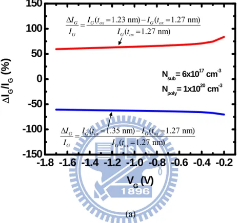
Fig. 2.5 Experimental and simulated gate current change versus gate voltage under -215 MPa longitudinal stress. The formulas used are inserted.
21
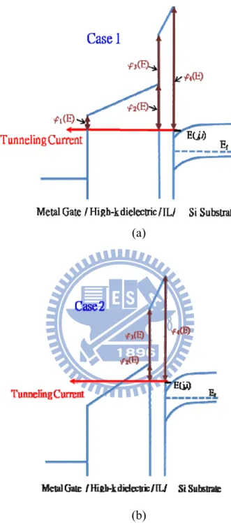
Fig. 2.6 Schematic energy band diagram of a p+ polysilicon/SiO2/n-Si system
biased in the inversion condition and stressed with uniaxial compressive conditions. The solid lines indicate the conduction and valence band edge without external stress. The dotted lines indicate the stress induced band edge shift of the conduction and valence band. The figure also shows the energy quantization effect in the inversion layer
xii
and the hole direct tunneling process from the inversion layer to the polysilicon gate.
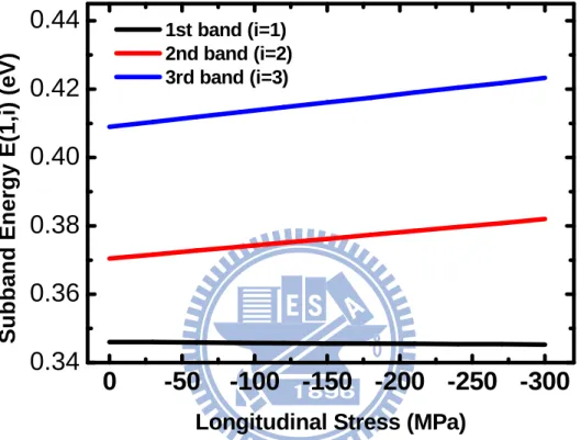
Fig. 2.7 Calculated energy levels versus stress for the top (first), second, and split-off (third) hole subbands.
23
Fig. 2.8 External stress dependent hole gate current data [2.1],[2.2] (symbols) used to examine the validity of the quantum strain simulator. The line represents the simulation result due to the strain altered valence-band splitting only.
24
Fig. 2.9(a) Simulated gate current change versus gate voltage for different gate oxide thicknesses. The formulas used are inserted.
25
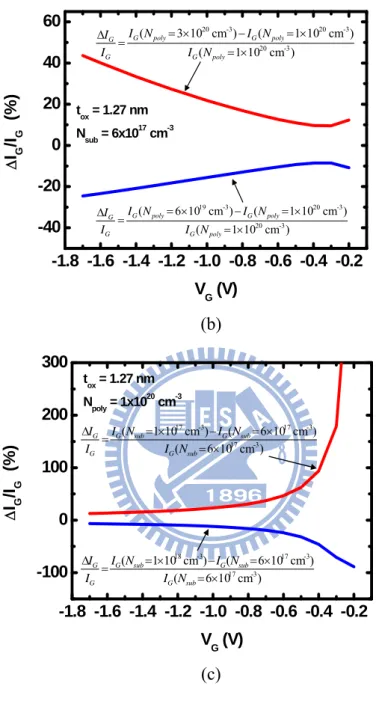
Fig. 2.9(b) Simulated gate current change versus gate voltage for different poly gate doping concentrations. The formulas used are inserted.
26
Fig. 2.9(c) Simulated gate current change versus gate voltage for different substrate doping concentrations. The formulas used are inserted.
26
Fig. 2.10 Simulated gate current change versus stress for several oxide thickness with respect to the gate current of = 0 case (that is, tox = 1.27 nm). Both the polysilicon doping concentration and substrate doping concentration are kept at the nominal values. Also shown for comparison are the experimental data (symbols) corresponding to the inset of Fig. 2.4.
27
Fig. 2.11 Simulated gate current change of zero poly stress with respect to poly stress of -215 MPa as a function of gate voltage for channel stress of -215 MPa. The formulas used are inserted.
28
Chapter 3
Fig. 3.1 Schematic of the energy band diagram of a metal-gate/high-k/IL/p-Si system biased in flat-band condition. The process and material parameters involved in this work are labeled.
40
Fig. 3.2(a) Schematic description of tunneling case 1: direct tunneling through both high-k and IL.
41
Fig. 3.2(b) Schematic description of tunneling case 2: F-N tunneling occurring in high-k layer.
41
xiii through IL.
Fig. 3.3 Simulated gate current and dlnIg/dVg in a wide range of gate voltage up
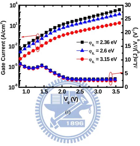
to 4 V. The parameters used in the calculation are: Fm = 4.48 eV, k =
1.65 eV, jIL = 3.15 eV, mk* = 0.18 mo, mIL* = 0.5 mo, tk = 2 nm, tIL = 1
nm, εk = 12.4 ε0, and εIL = 3.9 ε0.
43
Fig. 3.4(a) Simulated gate current Ig and dlnIg/dVg versus Vg for varying mk*. 44
Fig. 3.4(b) Simulated gate current Ig and dlnIg/dVg versus Vg for varying tk. 44
Fig. 3.4(c) Simulated gate current Ig and dlnIg/dVg versus Vg for varying tIL. 45
Fig. 3.4(d) Simulated gate current Ig and dlnIg/dVg versus Vg forvarying mIL*. 45
Fig. 3.4(e) Simulated gate current Ig and dlnIg/dVg versus Vg for varying εk. 46
Fig. 3.4(f) Simulated gate current Ig and dlnIg/dVg versus Vg for varying εIL. 46
Fig. 3.4(g) Simulated gate current Ig and dlnIg/dVg versus Vg for varying Fm. 47
Fig. 3.4(h) Simulated gate current Ig and dlnIg/dVg versus Vg for varying jk. 47
Fig. 3.4(i) Simulated gate current Ig and dlnIg/dVg versus Vg for varying jIL. 48
Fig. 3.5 Experimental (symbol) and simulated (line) Cg versus Vg for
TaC/HfSiON/SiON gate stacks n-MOSFET. The extrated parameters are: effective oxide thickness EOT = 1.4 nm; substrate doping concentration Nsub = 3μ1017 cm-3; metal-gate workfunction m = 4.48
eV.
49
Fig. 3.6 Comparison of the experimental (symbols) gate current and dlnIg/dVg
versus Vg with calculated (lines) results using two sets of parameters.
Red Line (new method): k = 1.1 eV, mk* = 0.03 mo, and mIL* = 0.95
mo. Blue Line (conventional method): k = 1.9 eV, mk* = 0.18 mo, and
mIL* = 0.3 mo. Other parameters are tIL = 1.3 nm and tk = 2.2 nm.
50
Fig. 3.7(a) Measured gate current at T = 300 and 373 K versus gate voltage for TaC/HfSiON/SiON n-MOSFETs.
51
Fig. 3.7(b) Comparison of simulated (line) gate current change of T = 373K with respect to T = 300K versus Vg with measured data (symbols). The
parameters used to create the red line (new method) and blue line (conventional method) in Fig. 3.6 are also used here.
51
Fig. 3.8 Comparison of the experimental (symbols) gate current and dlnIg/dVg
versus Vg with calculated (lines) results using two sets of tk and tIL for
the same EOT (1.4 nm). Red Line: tIL = 0.7 nm, tk = 3.2 nm, and mIL*
xiv
= 2.8 mo. Blue Line: tIL = 1.2 nm, tk = 2.3 nm, and mIL* = 1.1 mo. Other
parameters are mk* = 0.03 mo and jk = 1.1 eV.
Fig. 3.9 Comparison of the experimental (symbols) gate current and dlnIg/dVg
versus Vg with calculated (lines) results using two sets of εIL and jIL.
The same EOT (1.4 nm) is preserved. Red Line: mIL* = 0.95 mo, and tIL
= 1.3 nm. Blue Line: mIL* = 1.15 mo, and tIL = 1.1 nm. Other
parameters are k = 1.1 eV, mk* = 0.03 mo, and tk = 2.2 nm.
53
Fig. 3.10 Comparison of the experimental (symbols) gate current and dlnIg/dVg
versus Vg with calculated (lines) results with the potential drop in
high-k dielectric (DVk) as a parameter. Fitting parameters: Fm = 4.48
eV, k = 1.1 eV, jIL = 2.36 eV, mk* = 0.03 mo, mIL* = 0.95 mo, tk = 2.2
nm, tIL = 1.3 nm, εk = 12.4 ε0, and εIL = 7 ε0.
54
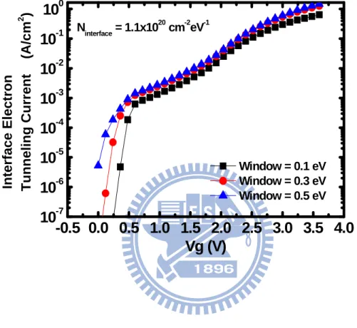
Fig. 3.11(a) Comparison of experimental data versus Vg with calculated direct and F-N tunneling current from inversion layer and interface states. Summation of both calculated tunneling current components is also shown. Parameters for calculating electron tunneling from interface states are Window = 0.5 eV and Ninterface = 1.1μ1020 cm-3eV-1. Other
parameters are the same as those used in the red line of Fig. 3.6.
55
Fig. 3.11(b) Comparison of the experimental (symbols) dlnIg/dVg versus Vg with calculated (lines) results of direct and F-N tunneling current from inversion layer and interface states. Parameters for calculating electron tunneling from interface states are Window = 0.5 eV and Ninterface =
1.1μ1020 cm-3eV-1. Other parameters are the same as those used in the
red line of Fig. 3.6.
55
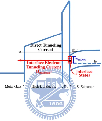
Fig. 3.12 Schematic band diagram showing the mechanism of electron tunneling from IL/Si interface states.
56
Fig. 3.13 Calculated electron tunneling current from IL/Si interface states versus Vg for different values of Window.
57
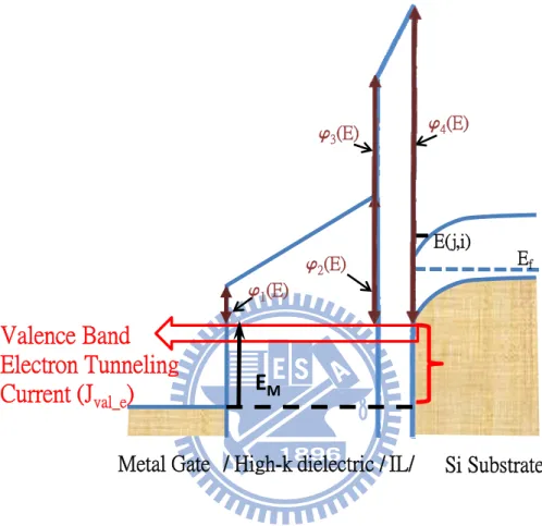
Fig. 3.14 Schematic band diagram showing the mechanism of valence band electron tunneling through high- stacks.
58
Fig. 3.15 Comparison of experimental data versus Vg with calculated valence electron tunneling current. Parameters for calculating valence electron tunneling current are m*IL_val = 0.655 m0, m*k_val = 0.03 m0, and
xv
m*valence = 0.65 m0. Other parameters are the same as those used in the
red line of Fig. 3.6.
Chapter 4
Fig. 4.1 Experimental (symbol) and simulated (line) Cg versus Vg for
TiN/HfO2/SiON gate stacks n-MOSFET. The extrated parameters are:
effective oxide thickness EOT = 0.75 nm; substrate doping concentration Nsub = 8μ1017 cm-3; metal-gate workfunction m = 4.5
eV.
66
Fig. 4.2 Experimental gate current versus gate voltage data, measured from different positions on wafer, for two temperatures.
67
Fig. 4.3 Schematic of the abrupt energy band diagram of a metal-gate/high-/IL/Si system for NMOS. The symbols serve as model parameters in calculation.
68
Fig. 4.4 Comparison of experimental (symbols) electron gate current and dlnIg/dVg versus Vg with calculated (lines) results. Fitting parameters
are k = 1 eV, mk* = 0.03 mo, mIL* = 1.3 mo, tk = 1.4 nm, and tIL = 0.9
nm.
69
Fig. 4.5(a) Schematic of the energy band diagram for a linear gradual transition layer.
70
Fig. 4.5(b) Schematic of the energy band diagram for a parabolic gradual transition layer.
70
Fig. 4.6(a) Comparison of experimental (symbols) electron gate current and dlnIg/dVg versus Vg with calculated (lines) results in the presence of a
linear transition layer. The same EOT (0.75 nm) is preserved. The fitting parameters are: for linear gradual transition layer, k = 1 eV, mk*
= 0.03 mo, mIL* = 0.75 mo, tk = 0.3nm , tmix = 1.41 nm, and tIL = 0.5
nm.
71
Fig. 4.6(b) Comparison of experimental (symbols) electron gate current and dlnIg/dVg versus Vg with calculated (lines) results in the presence of a
parabolic transition layer. The same EOT (0.75 nm) is preserved. The fitting parameters are: for parabolic gradual transition layer, k = 1 eV,
mk* = 0.03 mo, mIL* = 1.46 mo, tk = 0.2 nm , tmix = 1.33 nm, and tIL =
xvi 0.4 nm.
Fig. 4.7(a) TEM picture of TiN/HfO2/SiON gate stacks 72
Fig. 4.7(b) TEM picture of TaC/HfSiON/SiON gate stacks 72 Fig. 4.8 Comparison of experimental (symbols) electron gate current Ig and
dlnIg/dVg versus Vg with calculated (lines) results with and without the
transition layer. The same EOT (1.4 nm) is preserved. The fitting parameters are: for no transition layer (red lines), k = 1.1 eV, mk* = 0.03 mo, mIL* = 0.95 mo, tk = 2.2 nm, and tIL = 1.3 nm; for parabolic transition layer (blue lines), k = 1.1 eV, mk* = 0.02 mo, mIL* = 1.2 mo, tk = 0.5 nm, tmix = 2.1 nm, and tIL = 0.5 nm. Other parameters are the same: m = 4.48 eV and Nsub = 31017 cm-3.
73
Fig. 4.9(a) Schematic of the energy band diagram for case I: parabolic transition layer penetrates both high- layer and IL.
74
Fig. 4.9(b) Schematic of the energy band diagram for case II: parabolic transition layer mainly penetrates IL.
74
Fig. 4.9(c) Schematic of the energy band diagram for case II: parabolic transition layer mainly penetrates high- layer.
75
Fig. 4.10 Comparison of experimental (symbols) electron gate current and dlnIg/dVg versus Vg with calculated (lines) results in the presence of
three distribution cases of the parabolic transition layer. The same EOT (0.75 nm) is preserved. The fitting parameters are: for case I (red line),
k = 1 eV, mk* = 0.03 mo, mIL* = 1.46 mo, tk = 0.2 nm, tmix = 1.33 nm, and tIL = 0.4 nm; for case II (blue line), k = 1 eV, mk* = 0.02 mo, mIL* = 1.9 mo, tk = 1 nm, tmix = 0.95 nm, and tIL = 0.4 nm; and for case III (green line), k = 1 eV, mk* = 0.07 mo, mIL* = 1.11 mo, tk = 0.2 nm, tmix = 0.88 nm, and tIL = 0.7 nm.
76
Fig. 4.11 Schematic band diagram showing the mechanism of electron tunneling from IL/Si interface states.
77
Fig. 4.12(a) Comparison of experimental data versus Vg with calculated direct (DT) and F-N tunneling current from inversion layer and IL/Si interface states. Summation of both calculated tunneling current components is also shown. Parameters for calculating electron tunneling from interface states are Window = 0.11 eV and Ninterface =
xvii
1.1μ1020 cm-3eV-1. Other parameters are the same as those used in Fig.
4.4.
Fig. 4.12(b) Comparison of the experimental (symbols) dlnIg/dVg versus Vg with calculated (lines) results of direct and F-N tunneling current from inversion layer and interface states. Parameters for calculating electron tunneling from interface states are Window = 0.11 eV and Ninterface =
1.1μ1020 cm-3eV-1. Other parameters are the same as those used in Fig. 4.4.
78
Fig. 4.13(a) Comparison of experimental data versus Vg with calculated direct (DT) and F-N tunneling current from inversion layer and IL/Si interface states in the presence of a linear transition layer. Summation of both calculated tunneling current components is also shown. Parameters for calculating electron tunneling from interface states are Window = 0.11 eV and Ninterface = 1.8μ1020 cm-3eV-1. Other parameters
are the same as those used in Fig. 4.6(a).
79
Fig. 4.13(b) Comparison of the experimental (symbols) dlnIg/dVg versus Vg with calculated (lines) results of direct and F-N tunneling current from inversion layer and interface states in the presence of a linear transition layer. Parameters for calculating electron tunneling from interface states are Window = 0.11 eV and Ninterface = 1.8μ1020 cm-3eV-1. Other
parameters are the same as those used in Fig. 4.6(a).
79
Fig. 4.14(a) Comparison of experimental data versus Vg with calculated direct (DT) and F-N tunneling current from inversion layer and IL/Si interface states in the presence of a parabolic transition layer. Summation of both calculated tunneling current components is also shown. Parameters for calculating electron tunneling from interface states are Window = 0.11 eV and Ninterface = 1.8μ1020 cm-3eV-1. Other
parameters are the same as those used in Fig. 4.6(b).
80
Fig. 4.14(b) Comparison of the experimental (symbols) dlnIg/dVg versus Vg with calculated (lines) results of direct and F-N tunneling current from inversion layer and interface states in the presence of a parabolic transition layer. Parameters for calculating electron tunneling from interface states are Window = 0.11 eV and Ninterface = 1.8μ1020
cm-3eV-1. Other parameters are the same as those used in Fig. 4.6(b).
xviii Chapter 5
Fig. 5.1 Schematic of the energy band diagram of a metal-gate/high-/IL/n-Si system biased in flat-band condition. The process and material parameters for hole tunneling current calculation are labeled.
93
Fig. 5.2(a) Schematic description of tunneling case 1: direct tunneling through both high- and IL.
94
Fig. 5.2(b) Schematic description of tunneling case 2: F-N tunneling occurring in high-layer.
94
Fig. 5.2(c) Schematic description of tunneling case 3: only direct tunneling through IL.
95
Fig. 5.3 Schematic description of trap-assisted tunneling mechanism. The parameters used for TAT current calculation are labeled.
96
Fig. 5.4(a) Schematic description of gate-to-substrate electron tunneling mechanism. A region called Windowempty in IL/Si interface allows
electron tunneling from metal-gate to occupy.
97
Fig. 5.4(b) The band diagram of a metal-gate/high-/IL/n-Si system biased at flat band condition with the labels of parameters used for gate-to-substrate electron tunneling current calculation.
97
Fig. 5.5 Schematic band diagram showing the mechanism of hole tunneling from IL/Si interface states to metal-gate. A region called Window in IL/Si interface allows hole to occupy.
98
Fig. 5.6(a) Experimental (symbol) and simulated (line) Cg versus Vg for
TaC/HfSiON/SiON p-MOSFETs. The extrated parameters are: effective oxide thickness EOT = 1.5 nm; substrate doping concentration Nsub = 1μ1017 cm-3; metal-gate workfunction m = 4.48
eV.
99
Fig. 5.6(b) Experimental (symbol) and simulated (line) Cg versus Vg for
TiN/HfO2/SiON p-MOSFETs. The extrated parameters are: effective
oxide thickness EOT = 0.85 nm; substrate doping concentration Nsub =
6μ1017 cm-3; metal-gate workfunction
m = 4.5 eV.
99
Fig. 5.7 Experimental (solid symbol) and simulated (open symbol) Ig, Id, and Ib versus Vg for TaC/HfSiON/SiON p-MOSFETs. The current are
xix
measured with source, drain, and bulk tied to ground.
Fig. 5.8 Comparison of the experimental (symbols) hole tunneling current (Id) and dlnId/dVg versus Vg with calculated (lines) results using two sets
of parameters. Parameters for Red Line: k_h = 3 eV and m*IL_h = 0.67
mo; and for Blue Line (test): k_h = 3.5 eV and m*IL_h = 0.62 mo. Other
parameters are m*k_h = 0.03 mo, tIL = 1.3 nm and tk = 2.2 nm.
101
Fig. 5.9 Comparison of the experimental (symbols) gate-to-substrate electron tunneling current (Ib) and dlnIb/dVg versus Vg with calculated (lines)
results for different values of Windowempty. The parameters used here
are: k_m = 1.53 eV, m*k_e = 0.03 m0, m*IL_e = 0.95 mo, tIL = 1.3 nm and
tk = 2.2 nm.
102
Fig. 5.10(a) Comparison of experimental data versus Vg with calculated direct (DT) and F-N tunneling current from inversion layer and IL/Si interface states. Summation of both calculated tunneling current components is also shown. Parameters for calculating electron tunneling from interface states are Window = 0.35 eV and Ninterface =
6μ1019 cm-3eV-1. Other parameters are the same as those used in the
red line of Fig. 5.8.
103
Fig. 5.10(b) Comparison of the experimental (symbols) dlnId/dVg versus Vg with calculated (lines) results of direct and F-N tunneling current from inversion layer and interface states. Parameters for calculating electron tunneling from interface states are Window = 0.35 eV and Ninterface =
6μ1019 cm-3eV-1. Other parameters are the same as those used in the
red line of Fig. 5.8.
103
Fig. 5.11 Experimental (solid symbol) and simulated (open symbol) Ig, Id, and Ib versus Vg for TiN/HfO2/SiON p-MOSFETs. The current are
measured with source, drain, and bulk tied to ground.
104
Fig. 5.12(a) Comparison of the experimental (symbols) hole tunneling current (Id) versus Vg with calculated (lines) results of direct tunneling (DT), F-N tunneling, and TAT current. The parameter used in calculation are: k_h
= 1.95 eV, m*k_h = 0.08 mo, m*IL_h = 1.33 mo, xt_fav = 0.6 nm,
teffμcμNt = 3.3μ10-3, tk = 1.4 nm, and tIL = 0.9 nm.
105
xx
calculated (lines) results of direct tunneling (DT), F-N tunneling, and TAT current. The parameter used in calculation are: k_h = 1.95 eV,
m*k_h = 0.08 mo, m*IL_h = 1.33 mo, xt_fav = 0.6 nm, teffμcμNt =
3.3μ10-3, t
k = 1.4 nm, and tIL = 0.9 nm.
Fig. 5.13 Hole trap-assisted transmission probability though gate dielectric versus trap position (xt).
106
Fig. 5.14(a) Comparison of the experimental (symbols) hole tunneling current (Id) versus Vg with calculated (lines) results of direct tunneling (DT) and TAT current. The parameters used in calculation are: k_h = 3 eV, m*IL_h
= 0.8 mo, and teffμcμNt = 1.65μ10-3. Other parameters are the same as
those used in Fig. 5.12.
107
Fig. 5.14(b) Comparison of the experimental (symbols) dlnId/dVg versus Vg with
calculated (lines) results of direct tunneling (DT) and TAT current. The parameters used in calculation are: k_h = 3 eV, m*IL_h = 0.8 mo, and
teffμcμNt = 1.65μ10-3. Other parameters are the same as those used in
Fig. 5.12.
107
Fig. 5.15 Comparison of the experimental (symbols) gate-to-substrate electron tunneling current (Ib) and dlnIb/dVg versus Vg with calculated (lines)
results for different values of Windowempty. The fitting parameters are:
k_m = 1.45 eV, m*k_e = 0.03 m0, m*IL_e = 0.85 mo, tIL = 0.9 nm and tk =
1.4 nm.
108
Fig. 5.16(a) Comparison of experimental data versus Vg with not only calculated direct (DT) and F-N tunneling current from inversion layer and IL/Si interface states but also calculated TAT current. Summation of all components of calculated tunneling current is also shown. Parameters used in calculating electron tunneling current from interface states are Window = 0.32 eV and Ninterface = 1.1μ1022 cm-3eV-1. Other parameters
are the same with those used in Fig. 5.12.
109
Fig. 5.16(b) Comparison of the experimental (symbols) dlnId/dVg versus Vg with calculated (lines) results of direct and F-N tunneling current from inversion layer and interface states and TAT current. Parameters for calculating electron tunneling from interface states are Window = 0.32 eV and Ninterface = 1.1μ1022 cm-3eV-1. Other parameters are the same as
xxi those used in Fig. 5.12.
Fig. 5.17 Simulated hole gate tunneling results with/without transition layer versus Vg.
110
Chapter 6
Fig. 6.1 Calculated subband energy associated with field confinement (line) and structure confinement (line+symbol) versus Vg for tbody = 10 nm and
tbody = 20 nm.
119
Fig. 6.2(a) Calculated depletion charge density versus Vg for Nsub = 1μ1018 cm-3
and different tbody.
120
Fig. 6.2(b) Calculated depletion charge density versus Vg for Nsub = 2μ1018 cm-3
and different tbody.
120
Fig. 6.3(a) Comparison of numerically calculated subband energies (line + symbol) versus Vg with analytical ones (line) for tbody = 10 nm. Other
parameters and fitting factor used in calculation are labeled in figure.
121
Fig. 6.3(b) Comparison of numerically calculated subband energies (line + symbol) versus Vg with analytical ones (line) for tbody = 20 nm. Other
parameters and fitting factor used in calculation are labeled in figure.
121
Fig. 6.3(c) Comparison of numerically calculated subband energies (line + symbol) versus Vg with analytical ones (line) for tbody = 30 nm. Other
parameters and fitting factor used in calculation are labeled in figure.
122
Fig. 6.3(d) Comparison of numerically calculated subband energies (line + symbol) versus Vg with analytical ones (line) for tbody = 40 nm. Other
parameters and fitting factor used in calculation are labeled in figure.
122
Fig. 6.3(e) Comparison of numerically calculated subband energies (line + symbol) versus Vg with analytical ones (line) for tbody = 50 nm. Other
parameters and fitting factor used in calculation are labeled in figure.
123
Fig. 6.4(a) Comparison of numerically calculated surface potential bending (line + symbol) versus Vg with analytical ones (line). Parameters and fitting factor used in calculation are labeled in figure.
124
Fig. 6.4(b) Comparison of numerically calculated surface electric field (line + symbol) versus Vg with analytical ones (line). Parameters and fitting factor used in calculation are labeled in figure.
xxii
Fig. 6.5 Comparison of numerically calculated subband energies (line + symbol) versus Vg with analytical ones (line) for tbody = 10 nm. The
material parameters used here are different from those used in Fig. 6.3 but the best fitting values of hold the same with that used in Fig. 6.3.
125
Fig. 6.6 Comparison of numerically calculated gate tunneling current with analytical one versus Vg.
126
Fig. 6.7 for best subband fitting versus tbody for (110) surface. Linear fittings
of the are shown as lines and the fitting equations are labeled as well.
127
Fig. 6.8 Gate tunneling current change of gate tunneling current calculated with the linear fitting with respect to that calculated with best fitting versus tbody.
128
Fig. 6.9 for best subband fitting versus tbody for (001) surface. Linear fittings
of the are shown as lines and the fitting equations are labeled as well.
129
Fig. 6.10 Schematic cross-sectional view of FinFET device used in this work. 130 Fig. 6.11 Schematic of the abrupt energy band diagram of a
metal-gate/high-k/interfacial layer(IL)/Si system. The material parameters involved in this work are labeled.
131
Fig. 6.12 Experimental Cg data (symbols) and fitting result for double-gate structure (line) versus Vg for n-type FinFETs. The extracted process parameters are EOT = 0.8 nm, m = 4.6 eV and Nsub = 1μ1018 cm-3.
132
Fig. 6.13 Measured gate, source/drain, and bulk current at T = 300 and 328 K versus gate voltage. Weak temperature dependence of measured data indicates that the tunneling mecahanism dominates the gate leakage current. The source, drain, and bulk are all tied to ground.
133
Fig. 6.14 Comparison of experimental (symbols) electron gate current Ig and its dlnIg/dVg versus Vg with calculated (lines) results under the assumption of two abrupt layers (one of high- and one of IL; see Fig. 6.11) of high- metal-gate dielectric. Fitting parameters are k = 1.1 eV,
mk* = 0.02 mo, mIL* = 1.22 mo, tk = 1.2 nm, and tIL = 1 nm.
134
Fig. 6.15(a) TEM picture of high- metal-gate stack cited from the references [6.10], showing a transition region between IL and high- layer.
135
xxiii
[6.11], showing a transition region between IL and high- layer.
Fig. 6.16(a) Comparison of experimental (symbols) electron gate current Ig and dlnIg/dVg versus Vg with calculated (lines) results in the presence of a transition layer. The same EOT (0.8 nm) is preserved. The fitting parameters for linear gradual transition layer are k = 1.1 eV, mk* =
0.02 mo, mIL* = 0.8 mo, tk = 0.3nm , tmix = 1.31 nm, and tIL = 0.6 nm.
The insets show the schematic of the energy band diagram for a linear gradual transition layer.
136
Fig. 6.16(b) Comparison of experimental (symbols) electron gate current Ig and dlnIg/dVg versus Vg with calculated (lines) results in the presence of a transition layer. The same EOT (0.8 nm) is preserved. The fitting parameters for parabolic gradual transition layer are k = 1.1 eV, mk* =
0.02 mo, mIL* = 1.39 mo, tk = 0.4 nm , tmix = 1 nm, and tIL = 0.59 nm.
The insets show the schematic of the energy band diagram for a parabolic gradual transition layer.
137
Fig. 6.17 Comparison of experimental (symbols) electron gate current Ig and dlnIg/dVg versus Vg with calculated (lines) results in the presence of a parabolic gradual transition layer using two sets of fitting parameters. Red line (this work) came from the same parameters as used in Fig. 6.16(b) while blue line (conventional method) came from k = 1.5 eV,
mk* = 0.18 mo, mIL* = 0.93 mo, and the same physical thicknesses as
used in Fig. 6.16(b).
138
Fig. 6.18 The tunneling effective mass for hafnium based high- layer in the open literature and in our previous work versus effective oxide thickness (EOT). Solid symbols are for planar devices and open symbols are for FinFET devices.
139
Fig. 6.19 Schematic band diagram showing the mechanism of electron tunneling from IL/Si interface states.
140
Fig. 6.20(a) Comparison of experimental data versus Vg with calculated direct (DT) and F-N tunneling current from inversion layer and IL/Si interface states. Summation of both calculated tunneling current components is also shown. Parameters for calculating electron tunneling from interface states are Window = 0.17 eV and Ninterface =
xxiv
1.1μ1020 cm-3eV-1. Other parameters are the same as those used in Fig.
6.14.
Fig. 6.20(b) Comparison of the experimental (symbols) dlnIg/dVg versus Vg with calculated (lines) results of direct and F-N tunneling current from inversion layer and interface states. Parameters for calculating electron tunneling from interface states are Window = 0.17 eV and Ninterface =
1.1μ1020 cm-3eV-1. Other parameters are the same as those used in Fig. 6.14.
141
Fig. 6.21(a) Comparison of experimental data versus Vg with calculated direct (DT) and F-N tunneling current from inversion layer and IL/Si interface states in the presence of a linear transition layer. Summation of both calculated tunneling current components is also shown. Parameters for calculating electron tunneling from interface states are Window = 0.17 eV and Ninterface = 2.5μ1020 cm-3eV-1. Other parameters
are the sameas those used in Fig. 6.16(a).
142
Fig. 6.21(b) Comparison of experimental data versus Vg with calculated direct (DT) and F-N tunneling current from inversion layer and IL/Si interface states in the presence of a parabolic transition layer. Summation of both calculated tunneling current components is also shown. Parameters for calculating electron tunneling from interface states are Window = 0.17 eV and Ninterface = 2μ1020 cm-3eV-1. Other
parameters are the same as those used in Fig. 6.16(b).
143
Fig. 6.22 Experimental (symbols) and simulated (line) Cg versus Vg for
nMOSFETs. The discrepancy from experimental data is caused by large gate leakage current across large gate dielectric area.
144
Fig. 6.23 Comparison of experimental (symbols) electron gate current and dlnIg/dVg versus Vg with calculated (lines) results. The inset shows that surface orientation does not strongly affect gate tunneling current. The fitting parameters are k = 1.1 eV, mk* = 0.02 mo, mIL* = 1.39 mo,
tk = 0.4 nm , tmix = 1 nm, and tIL = 0.54 nm.
145
Fig. 6.24 Comparison of experimental data versus Vg with calculated valence electron tunneling current. Parameters for calculating valence electron tunneling current are: for red line, Window = 0 eV, m*IL_val = 0.6 m0,
m*k_val = 0.02 m0, and m*valence = 0.65 m0; and for blue line, Window =
xxv
0.21 eV, m*IL_val = 0.73 m0, m*k_val = 0.02 m0, and m*valence = 0.65 m0.
Other parameters are the same as those used in Fig. 6.14.
Fig. 6.25 Schematic band diagram showing the mechanism of valence band electron tunneling through high- stacks.
xxvi
List of Symbols
Cg Gate capacitance
Ig Gate leakage current Id Drain leakage current
Ib Substrate leakage
EOT Effective oxide thickness
IL Interfacial layer
Nsub Substrate doping concentration
Npoly Poly gate doping concentration
N(j,i) Hole density per unit area of the j-th subband in the i-th valence band
Ninterface Interface trap density
Nt Trap density
Qdepl Depletion charge density
tox Physical oxide thickness
tIL Physical IL thickness
tk Physical high- layer thickness tmix Physical thickness of transition layer
tbody Distance between two controlled gate stacks
tstack Physical thickness of gate stacks (tk+tIL)
xt Trap distance apart from IL/Si interface
xt_fav Specific favorable trap position can contribute maximum TAT current
teff Effective thickness that the trap-assisted current flow mainly
W Channel width
Wmask Mask gate width
L Channel length
Fin Height Fin sidewall height of a FinFET a gate to STI spacing
Vthermal Thermal velocity (107 cm/sat room temperature)
Channel stress
c Trap cross section area
E(j,i) Energy of the j-th subband in the i-th valence band EVi Energy of the i-th valence band
EF Fermi level
Fs Silicon surface electric field strength
Fk Electric field in high- layer
FIL Electric field in IL
xxvii
mzhi Hole out-of-plane effective mass associated with the i-th valence band
mdhi 2-D DOS (density of states) effective mass of the i-th valence band
mox* Hole effective mass in oxide
mk* Tunneling effective mass in high- layer
mIL* Tunneling effective mass in IL
m*k_h Hole tunneling effective mass in high- layer
m*IL_h Hole tunneling effective mass in IL
m*M Effective mass in metal (1 m0)
f Impact frequency on the Si/SiO2(IL) interface Pt(E(j,i)) Hole transmission probability across the SiO2 film
TWKB Transmission probability across the high- film
TR Reflection correction factor
J Electron/hole direct/F-N tunneling current Jinterface Tunneling current from IL/Si interface states
JTAT Trap-assisted-tunneling current
JMGe Metal gate-to-substrate electron tunneling current
m Metal workfunction
k Band offset of high- layer with respect to silicon conduction band
IL Band offset of IL with respect to silicon conduction band
k_h Valence band offset of high- layer to silicon valence band
IL_h Valence band offset of IL to silicon valence band
k_e Conduction band offset of high- layer to silicon conduction band
IL_e Conduction band offset of IL to silicon conduction band
k_m (k_e + (m-s))
IL_m (IL_e + (m-s))
t Trap energy with respect to the valence band of high- layer or IL
depl(Vg) Potential band bending across depletion region versus gate voltage bias
Window A local region, sited in the forbidden band gap with respect to conduction (valence) band edge, allowing electrons (holes) to populate
Windowempty A region in IL/Si interface allows electron tunneling from metal-gate to occupy
si Silicon permittivity
ox Permittivity of SiO2
k Permittivity of high- layer
IL Permittivity of IL
mix(n) Permittivity of n-th abrupt barrier k Electron affinity of high-k layer
IL Electron affinity of IL kB Boltzmann’s constant
1
Chapter 1
Introduction
1.1 Background
Aggressive scaling of complementary metal-oxide-semiconductor field-effect transistors (CMOSFETs) continues for the purpose of reducing average cost per transistor, boosting device performance, and enhancing chip’s functionality with higher transistor density. Scaling of CMOSFETs is usually accompanied with equivalent oxide thickness (EOT) reduction for maintaining the gate control over the channel. However, the downward scaling of EOT directly increases the power consumption of the device because the leakage current increases significantly with decreasing physical thickness of gate dielectric. Advanced technologies are developed to overcome the leakage problem while keeping constant transistor performance improved. One of the crucial technologies is high- materials that are adopted in gate dielectric manufacturing [1.1],[1.2] with aim to reduce gate leakage. Due to thicker physical thickness of high- layer with the same EOT manufactured from conventional SiO2 dielectric, the leakage problem was mitigated. Furthermore, a
tri-gate structure (FinFET) has attracted much attention in recent years [1.3]-[1.16]. Utilizing the strong gate control ability of tri-gate structure, the pressure on EOT scaling can be considerably released. Hence, the low gate leakage level can be hold as the scaling continues for FinFET structure.
Strain technologies are also extensively used to boost the transistor performance [1.17]-[1.20]. Due to serious power consumption issue originating from significant tunneling current in modern-day device, direct tunneling current across the gate oxide of MOSFETs has been extensively studied in the presence of an external
2
mechanical stress applied during the measurement of this current [1.21]-[1.23]. Those studies attributed the external stress induced gate leakage change to both change of the carrier repopulation and the effective SiO2/Si barrier height due to
strain induced band splitting. However, process-induced stress may affect some process parameters rather than simply the strain altered valence-band splitting. For example, the study has proven that oxidation rate can be affected by stressing [1.24]. The effects of process-induced variation on direct tunneling current have not been fully addressed. Hence, it remains unclear whether the trend of the hole direct tunneling with the external stress, as claimed in the literature [1.21],[1.22], could hold for the process induced case. In this work, the test samples are designed with different dimensions of gate edge to STI edge spacing in order to alter level of stress in channel. We find that the experimental hole gate direct tunneling current of p-MOSFETs versus STI (shallow trench isolation) induced longitudinal compressive stress, which does not appear to follow the trend [1.21],[1.22], is caused by the strain altered valence-band splitting alone. The physical explanation of the deviation between process- and external induced hole direct tunneling current change is systematically drawn. Furthermore, we find that direct tunneling current modeling can serve as a sensitive detector of process parameters.
The dimensions of CMOS continue to shrink such as to meet the requirements of Moore’s law that the number of transistors in a chip counts double every two years. To keep the device performance improvement, the scaling procedure is not only to shorten the gate length but also scale the thickness of gate dielectric and depletion region in gate and substrate. One of most troublesome issues in scaling path is the unacceptable power consumption due to significant tunneling current effect as the oxide/oxynitride thickness is reduced down to around one nanometer. To solve this power consumption issue, high- materials were adopted in gate dielectric
3
manufacturing [1.1],[1.2]. Comparing SiO2 gate dielectric counterpart, the high-
can achieve the same EOT but with thicker physical thickness of gate dielectric. Therefore, the leakage current can be effectively reduced in MOSFETs with high- gate dielectric. In addition, high- gate dielectric is usually integrated with metal gate in order to eliminate the poly depletion to get lower capacitance equivalent thickness (CET). Hence, metal-gate/high- gate stacks system has replaced poly-gate SiO2 gate dielectric system in advanced VLSI technologies. High- gate stacks
usually include an ultra-thin interfacial layer (IL) for high quality Si-SiO2 interface
beneath the high- material. Accurate modeling and characterization of the tunneling current through high- stacks is crucial to understanding the limitation in power consumption of the devices with high- metal-gate. Many studies [1.25]-[1.33] have been dedicated to modeling direct tunneling through high- gate stacks of MOSFETs. However, these works, which neglected the transition of direct tunneling and Fowler-Nordheim (F-N) tunneling across high- layer [1.34], may lead to wrong fitting parameters. Because the band offset of high- materials to silicon is usually smaller than that of SiO2 [1.35], the transition between direct tunneling and F-N
tunneling is potentially important in the modeling of tunneling current through high- gate stacks. In this work, combining the gate tunneling current fitting with its dlnI/dVg fitting, the gate tunneling current fitting guideline for accurately extracting the parameters of high- layer is created. The validity of this new proposed gate tunneling fitting guideline has been proven throughout this work, along with TaC/HfSiON/SiON and TiN/HfO2/SiON gate stacks n (p)-MOSFETs and
metal-gate/HfO2 based high- layer/IL n-FinFET serving as test samples.
Furthermore, the gate leakage current modeling at low gate bias is still a challenge work. Hence, we propose a model for simulating electron tunneling from IL/Si interface states in forbidden band gap of Si to metal gate, with aim to explain the
4
physical meaning of gate current at low gate bias. The validity of this extra modeling is verified experimentally throughout this work.
Following the fitting guideline established by electron tunneling current fitting of n-MOSFET with high- gate stacks [1.36], good reproduction of hole tunneling current is achieved and the corresponding material parameters are accurately extracted. However, based on our measured tunneling current data, we find that gate-to-substrate electron tunneling current (Ib) dominates overall gate leakage current at particular range of gate bias. This phenomenon is caused by the fact that tunneling barrier height seen by holes at inversion layer is higher than that seen by electrons in metal gate. Although Ib is getting importance for metal-gate high- p-MOSFETs at inversion condition, its fitting work is still lacking. In this work, the hole tunneling current from both inversion layer and IL/Si interface states and gate-to-substrate electron tunneling at inversion condition in metal-gate high- p-MOSFETs are excellently modeled.
As the scaling of CMOSFETs continues, maintaining the ability of gate control over channel is challenging. Short channel effect (SCE) and DIBL are serious issues in nano-scaled conventional planar devices. Under the circumstances, a transistor with 3-D multi-gate structure (FinFET) was developed [1.3]-[1.16]. The FinFET transistors have superior capability in gate control over planar transistors as the gate length becomes shorter and shorter [1.3],[1.7],[1.9]-[1.10]. Excellent short channel effect control was proven for gate length of less than 25 nm [1.9]-[1.10]. Owing to the strong ability of gate control, strict demand of EOT scaling is mitigated in FinFETs. In other words, the power consumption (due to gate tunneling leakage) issue in FinFET devices gets better control than that in planar ones. Although the FinFET structures were widely discussed in the open literature, the fitting work of gate tunneling leakage current in FinFET devices was rarely addressed [1.37]. In this
5
work, with an analytical model for double-gate structure, reproduction of experimental gate tunneling current in metal-gate high- gate stacks nFinFET is achieved. The already established gate tunneling current fitting guideline for planar devices [1.36] has been successfully applied in fitting experimental gate tunneling current in metal-gate high- gate stacks FinFETs, leading to underlying process parameters.
1.2 Organization of this Dissertation
Introduction is given in Chapter 1. In Chapter 2, a strain quantum simulator is established. To control the process-induced channel stress, different gate edge to STI edge spacings are designed. Hole tunneling currents versus Vg for different STI-induced channel stresses are measured. Then, the physical origin of experimental hole current change due to process-induced stress is determined in terms of ultra-small oxide thickness change with internal stress.
Chapter 3 and 4 clearly describe direct and F-N tunneling models for metal-gate high- nMOSFETs. Reproduction of experimental tunneling current measured from TaC/HfSiON/SiON and TiN/HfO2/SiON gate stacks n-MOSFETs is achieved. A new
advanced fitting approach by combining conventional Ig-Vg and Cg-Vg curve fittings with its dlnIg/dVg fitting is established. The ability and validity of this new gate tunneling approach are shown. Then, the fitting guideline of gate tunneling current for metal-gate high- nMOSFETs is established as well. Furthermore, the physical origin of experimental gate leakage at low gate bias is captured accordingly. In Chapter 5, the theory and model of hole direct tunneling current for metal-gate
high- pMOSFETs are presented. TaC/HfSiON/SiON and TiN/HfO2/SiON gate
stacks pMOSFETs serve as test devices. Owing to the dominance of the gate-to-substrate tunneling current in overall gate current leakage, the model used for
6
calculating metal-to-substrate electron tunneling current at inversion condition is constructed and discussed. Direct and F-N tunneling currents originating from hole inversion layer and IL/Si interface states are combined with TAT current component to explain experimental result.
Chapter 6 focuses on fitting gate tunneling current of FinFET transistors with metal-gate high- stacks. A simple simulator for double-gate structure is established and used to reproduce the tunneling current components through gate dielectric of FinFET. The validity of the simulator in combination of analytical tunneling model is confirmed for different fin widths. Good reproduction of electron gate leakage current versus Vg curve in a wide range of six decades is obtained.
Finally, in Chapter 7, the conclusions of the work are given and the major contributions are highlighted.
7
Chapter 2
Enhanced Hole Gate Tunneling Current in Process-Induced
Uniaxial Compressive Strained p-MOSFETs
2.1 Introduction
Hole direct tunneling current across the gate oxide of p-MOSFETs has been extensively studied in the presence of an external mechanical stress applied during the measurement of this current [2.1]-[2.3]. The corresponding gate oxide thickness change due to the effect of Poisson’s ratio has been shown to be negligible in magnitude; for example, in the citation [2.1], around 0.03 % change in the gate oxide thickness has been estimated for an external stress of 300 MPa. Therefore, the physical gate oxide thickness essentially remains unchanged, regardless of the externally applied stress. Under the circumstances, the induced gate current variation can be properly attributed, through the change in both the carrier repopulation and the effective SiO2/Si barrier height, to the strain induced valence-band splitting. It has
been therefore argued that the hole gate direct tunneling current decreases with the external compressive stress [2.1],[2.2].On the other hand, for the case of p-MOSFETs undergoing a process-induced (internally applied), mobility-boosting mechanical stress during the manufacturing of the device, hole gate direct tunneling current may encounter complicated situations (gate oxide thickness change due to strain dependence of the oxidation rate, for example), rather than simply the strain altered valence-band splitting. So far, it has been unclear whether the decreasing trend of the hole direct tunneling with the compressive stress, as claimed in the literature [2.1],[2.2], could hold for the internal case. Thus, the ability to distinguish the external stress effect from the internal one and/or find the similarities between the two is
8 crucial.
In this work, we will elaborate on the above subject. First of all, we will present the experimental hole gate direct tunneling current of p-MOSFETs under STI (shallow trench isolation) induced longitudinal compressive stress, which does not appear to follow the trend [2.1],[2.2] caused by the strain altered valence-band splitting alone. A quantum strain simulator will be developed to resolve this contradictory issue. The validity of the simulator will be examined in detail. Then, the quantum simulator will be combined, in a systematic manner, with the experimental data in order to determine the underlying physical origin.
2.2 Experimental
P-channel MOSFETs as schematically shown in Fig. 2.1 were fabricated using a state-of-the-art manufacturing process. In this process, the STI induced compressive stress was applied prior to the growth of the gate oxide and the source/drain implantation. The nominal process parameters were obtained by the capacitance-voltage fitting: p+ polysilicon doping concentration N
poly = 1 × 10 20 cm-3, physical gate oxide thickness tox = 1.27 nm, and n-type substrate doping concentration
Nsub =6 × 10 17 cm-3. The gate width to length ratio was fixed at W/L = 10 m /1 m. The devices were formed on (001) wafer with the channel length direction along <110>. The use of the wide structures ensures that the transverse channel stress can be reasonably ignored. To control the longitudinal channel stress, the gate to STI spacing as labeled a in Fig. 2.1 was drawn with three values of 10.0, 0.495, and 0.21 m. The corresponding stress magnitude can be determined via the piezoresistance coefficients. First of all, the peak hole mobility at VD = - 0.025 V was measured across the wafer. The relative change of the average peak hole mobility was then obtained with respect to that of a = 10 m, as plotted in Fig. 2.2 versus stress. Here, the state-of-the-art
9
inversion-layer piezoresistance coefficient for holes, as quoted elsewhere [2.2], was employed as demonstrated by a straight line in the figure. The corresponding longitudinal channel stress is therefore determined to be around -120 and -215 MPa for a = 0.495 and 0.21 m, respectively. To testify to the validity of the extracted stresses, one empirical formula, which connects the layout parameters to the stress quantities, was also cited elsewhere [2.4]: (a) = (amin) (1+Vm(aamin)/a), where
min
a is the minimum gate-to-STI spacing and Vm is the maximum variation for a
with respect to (amin). Excellent fitting was achieved with Vm= -1.02, as
shown in the inset of Fig. 2.2.
To examine the poly stress, the threshold voltage was also measured across the wafer with the results in Fig. 2.3 in terms of the average and standard deviation of the distribution. The threshold voltage variation appears to be a weak function of the gate-to-STI spacing and its trend looks irregular, prohibiting the poly stress from being determined. However, in our previous work [2.9], the electron direct tunneling data confirm the existence of a lateral STI induced stress in the polysilicon, and since the gate oxide is rather thin, the lateral stress near the polysilicon surface is reasonably close to that of the underlying silicon. The same wafer was used in this study and thereby the poly stress was made equal to the channel stress. Extra evidence will be given later.
The hole gate direct tunneling current was measured in inversion with the source, drain, and substrate tied to the ground. Strikingly, the gate current versus gate voltage characteristics measured across the whole wafer do not appear to deviate from each other. This situation is displayed in Fig. 2.4for several samples with different a values and different device positions. Obviously, it is difficult to distinguish the measured