國
國
國
國 立
立
立
立 交
交
交
交 通
通
通 大
通
大
大
大 學
學
學
學
電子工程學系
電子工程學系
電子工程學系
電子工程學系 電子研究所
電子研究所
電子研究所
電子研究所
博
博
博
博 士
士
士 論
士
論
論 文
論
文
文
文
低溫複晶矽薄膜電晶體
低溫複晶矽薄膜電晶體
低溫複晶矽薄膜電晶體
低溫複晶矽薄膜電晶體負偏壓溫度不穩定
負偏壓溫度不穩定
負偏壓溫度不穩定
負偏壓溫度不穩定
與天線效應之研究
與天線效應之研究
與天線效應之研究
與天線效應之研究
Study on Negative Bias Temperature Instability
and Antenna Effect of Low-Temperature
Polycrystalline Silicon Thin-Film Transistors
低溫複晶矽薄膜電晶體
低溫複晶矽薄膜電晶體
低溫複晶矽薄膜電晶體
低溫複晶矽薄膜電晶體負偏壓溫度不穩定
負偏壓溫度不穩定
負偏壓溫度不穩定
負偏壓溫度不穩定
與天線效應之
與天線效應之
與天線效應之
與天線效應之研究
研究
研究
研究
Study on Negative Bias Temperature Instability and
Antenna Effect of Low-Temperature Polycrystalline
Silicon Thin-Film Transistors
研 究 生:陳志仰
Student:Chih-Yang Chen
指導教授:雷添福 博士 Advisor:Dr. Tan-Fu Lei
國立交通大學
電子工程學系 電子研究所
博士論文
A Dissertation
Submitted to Department of Electronics Engineering
and Institute of Electronics
College of Electrical and Computer Engineering
National Chiao Tung University
In Partial Fulfillment of the Requirements
For the Degree of
Doctor of Philosophy
in
Electronics Engineering
September 2007
Hsinchu, Taiwan, Republic of China
低溫複晶矽薄膜電晶體負偏壓溫度不穩定
低溫複晶矽薄膜電晶體負偏壓溫度不穩定
低溫複晶矽薄膜電晶體負偏壓溫度不穩定
低溫複晶矽薄膜電晶體負偏壓溫度不穩定
與
與
與
與天線效應
天線效應
天線效應之研究
天線效應
之研究
之研究
之研究
學生
學生
學生
學生:
:
:
: 陳
陳
陳 志
陳
志
志 仰
志
仰
仰
仰
指導教授:
指導教授
指導教授
指導教授
:
:
: 雷
雷
雷 添
雷
添 福
添
添
福
福
福 博士
博士
博士
博士
國立交通大學
國立交通大學
國立交通大學
國立交通大學
電子工程學系
電子工程學系
電子工程學系
電子工程學系 電子研究所博
電子研究所博
電子研究所博
電子研究所博士班
士班
士班
士班
摘
摘
摘
摘 要
要
要
要
此論文探討了低溫複晶矽薄膜電晶體(LTPS TFTs)的可靠度,包含了負偏壓溫度不 穩定(NBTI)與天線效應(antenna effect)。此外,我們也針對天線效應對低溫複晶矽薄膜 電晶體負偏壓溫度不穩定的影響進行探討。最後,我們提出一個新模型來解釋負偏壓 溫度不穩定與熱載子效應(hot-carrier effect)相結合下對元件特性的影響。 首先,我們證實負偏壓溫度不穩定對 p 型通道低溫複晶矽薄膜電晶體可靠度而言 是重要的可靠度問題,在負偏壓溫度不穩定應力(NBTI stress)測試下,我們發現臨界電場效電晶體(MOSFET)的負偏壓溫度不穩定模型,提出了一個新模型來解釋低溫複晶矽 薄膜電晶體負偏壓溫度不穩定的劣化機制。我們也利用電荷幫浦(charge pumping)的技 術來探討此劣化機制,分析出基底(bulk)缺陷態位的特性(包含晶界缺陷態位與界面缺陷 態位),並萃取出固定氧化層電荷(fixed oxide charge)的密度。因此,低溫複晶矽薄膜電 晶體之負偏壓溫度不穩定劣化機制更確信是由界面缺陷態位、晶界缺陷態位與固定氧 化層電荷的產生所造成。 接著,我們針對低溫複晶矽薄膜電晶體設計不同的天線結構,來探討天線效應對 元件特性和可靠度的影響。實驗結果發現,當元件具有較大的天線面積時,元件特性 會發生不穩定的現象,特別是造成臨界電壓的不均勻分佈,另外在閘極偏壓應力 (gate-bias stress)與熱載子應力下也有較差的可靠度。此外,我們也研究天線效應對負偏 壓溫度不穩定的影響,並發現天線效應會加速負偏壓溫度不穩定的程度,導致元件有 較差的臨界電壓、次臨界擺幅(subthreshold swing)、場效載子遷移率(field-effect mobility) 和驅動電流(drive current)。 最後,我們研究 p 型通道低溫複晶矽薄膜電晶體在負偏壓溫度不穩定與熱載子應 力測試下的劣化機制。在固定的閘極電壓應力下,我們探討在不同的汲極電壓應力對 元件劣化的影響。實驗結果顯示,在低的汲極電壓應力下,元件的劣化主要是負偏壓 溫度不穩定所主導;在高的汲極電壓應力下,負偏壓溫度不穩定會被抑制,元件劣化 機制轉由熱載子應力所主導。為了定量分析負偏壓溫度不穩定與熱載子應力兩者對元 件所造成的劣化,我們針對負偏壓溫度不穩定與熱載子應力的模型加以修改,並提出 了一個與實驗結果相吻合的新模型。
Study on Negative Bias Temperature Instability and
Antenna Effect of Low-Temperature Polycrystalline
Silicon Thin-Film Transistors
Student: Chih-Yang Chen
Advisor: Dr. Tan-Fu Lei
Department of Electronics Engineering &
Institute of Electronics
National Chiao Tung University
ABSTRACT
In this thesis, the reliability of low-temperature polycrystalline silicon thin-film transistors (LTPS TFTs) was studied, including negative bias temperature instability (NBTI) and antenna effect. In addition, the impacts of antenna effect on the NBTI behaviors of LTPS TFTs were explored. Finally, a new model was proposed to explain the combined NBTI and hot-carrier effects on the device characteristics.
analyzed and found to be the reverse process of diffusion-controlled electrochemical reactions. By expanding the model proposed for metal-oxide-semiconductor field-effect transistors (MOSFETs), a new model is introduced to explain the NBTI-degradation mechanism of LTPS TFTs. The mechanism is also analyzed by a charge-pumping technique to directly characterize the bulk trap properties (including grain-boundary and interface trap-state density) in LTPS TFTs. The fixed-oxide-charge density is also extracted and the NBTI degradation can therefore be confirmed to be caused by the generation of interface trap states, grain-boundary trap states and fixed oxide charges.
Second, LTPS TFTs having different antenna structures were used to study the influence of antenna effect on the performance and reliability of the devices. Experimental results show that performance instability of the devices occurs for those samples having relatively large-area antennas, especially causing non-uniform distribution of the threshold voltages. Devices having larger antenna areas also show a more degraded reliability under gate-bias stress and hot-carrier stress (HCS) than those of the samples having smaller antenna areas. In addition, the impact of the antenna effect on the NBTI behavior of LTPS TFTs is investigated. The antenna effect accelerates NBTI, and results in an enhanced degradation of threshold voltage, subthreshold swing, field-effect mobility and drive current.
Finally, degradation mechanisms of p-channel LTPS TFTs upon NBTI and HCS were investigated. Under a fixed stress gate voltage, the dependence of the device degradation on the stress drain voltage was analyzed. At a low stress drain voltage, the device degradation is dominated by the NBTI; at a high stress drain voltage, NBTI is retarded, and HCS dominates the degradation. To quantify the combined effects of NBTI and HCS, a modified model, based on the empirical NBTI and HCS models, is proposed, which is demonstrated to be consistent with the experimental results.
誌
誌
誌
誌
謝
謝
謝
謝
此論文的完成,要感謝的人實在太多了!沒有眾人的支持與鼓勵,就無法成就這 一切。首先,感謝我的指導教授-雷添福博士,對我的指導與教誨,讓我學習到研究 的態度及方法,更重要的是教導我待人處世之道,令我獲益良多。 感謝王獻德學長的提攜,帶我進入薄膜電晶體的領域,並提供新穎的研究方向; 感謝統寶光電林孝義學長、葉冠麟學長及陳維成學長,在百忙之中提供實驗上的協助; 感謝李介文學長,在我研究遇到瓶頸時提供寶貴的意見;還要感謝伯浩和統億,在實 驗量測上的協助及實驗數據上的分析,此論文是我們一起努力的成果。 感謝在研究中曾給我幫助的前輩們,特別是元件計測實驗室的彭作煌先生、電子 教學實驗室的彭兆光先生,與奈米中心的徐秀鑾小姐、黃月美小姐、林素珠小姐、楊 月嬌小姐、范秀蘭小姐、陳悅婷小姐、何惟梅小姐、劉曉玲小姐,以及國家奈米元件 實驗室的工程師們,因為有你們的大力幫忙,讓我在研究及學習上事半功倍,在此獻 上我最深的敬意。 感謝薄膜與量測實驗室的所有人員:李名鎮學長、余正明學長、李宗霖學長、王 哲麒學長、謝明山學長、陳建豪學長、楊紹明學長、游信強學長、林育賢學長、郭柏 儀學長、謝德慶學長、李美錡學姐、賴久盟學長、謝松齡學長、羅韋翔學長、林余俊 學長和江國誠學長,感謝你們帶我進入半導體領域,並給予指導與勉勵。感謝同窗好 友家文及任逸,在課業上的砥礪及生活上的協助。感謝小馬、俊嘉、宗元、源竣、梓 翔、錦石、仕傑、文呈、久騰、明爵、哲綸、子恆、張婷、冠良、文彥、小春、伊容, 實驗室因為有你們而充滿歡樂,並陪我度過漫長的研究歲月。 由衷感謝我敬愛的父母,陳忠明先生與呂綿女士,感謝你們提供一個溫暖的家, 以及二十多年來的養育之恩,由於你們的付出,我才能無後顧之憂地完成學業;感謝 大哥炫文、大嫂詩茹、二哥峰志、二嫂春蘭,在學業上的支持與生活上的照顧;感謝
Contents
Abstract (Chinese) ………...………I
Abstract (English) ……….III
Acknowledgment (Chinese)………...V Contents ………...VI
Table Lists………...IX Figure Captions………...…………X
Chapter 1
Introduction...1
1.1 Overview of Thin-Film Transistors………. ………...…….………...1
1.1.1 Advantages of Poly-Si TFTs……….………...……….2
1.1.2 Crystallization of α-Si Thin Films………....……….3
1.2
Reliability Issues in LTPS TFTs………...………..……...5
1.2.1 Negative Bias Temperature Instability………...…….………..5
1.2.2 Plasma-Induced Damage………...…….………...9
1.2.3 Hot-Carrier Effect... ………...……….…10
1.3 Motivation……….………...………11
1.4 Thesis Organization ………….………….………...…...……...….13
Chapter 2
Negative Bias Temperature Instability in Low-Temperature
Polycrystalline Silicon Thin-Film Transistors…...20
2.1 Introduction ……….……….………...……...…..20
2.2 Experiments …...………..….………...……….………...…………..21
2.3 Results and Discussion……….………..……….….22
2.3.2 Analysis of the Threshold-Voltage Shift..………...……24
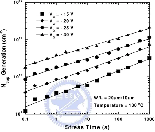
2.3.3 Analysis of the Grain-Boundary Trap-State Generation...……….….26
2.3.4 Analysis of the Interface-Trap-State Generation…...………...27
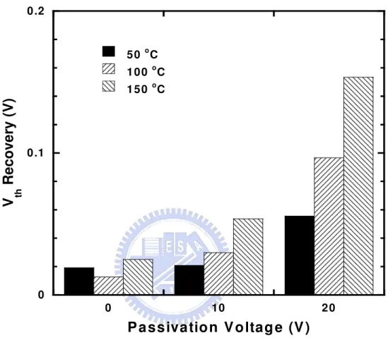
2.3.5 Recovery Behavior of NBTI………...28
2.3.6 Physical Model of NBTI……….………..……...29
2.4 Summary ……….………...…31
Chapter 3
Analysis of Negative Bias Temperature Instability in Body-Tied
Low-Temperature
Polycrystalline
Silicon
Thin-Film
Transistors...58
3.1 Introduction ……….……….………...……….58
3.2 Experiments ………...………..…………...……….60
3.3 Results and Discussion ………..………...……61
3.3.1 Basic Charge-Pumping-Current Characteristics……….……...61
3.3.2 Device Degradation Due to NBTI…..………...…62
3.3.3 Analysis of the Bulk Trap-State Generation…...……….……...63
3.3.4 Analysis of the Fixed-Oxide-Charge Generation.……..…...………...…….65
3.3.5 Physical Model of NBTI…...………...….66
3.4 Summary………..………...………...…..67
4.3.2 Fixed AR/Various Device Sizes……….………..……98
4.4 Summary ……….………...………...……….101
Chapter 5
Antenna Effect Enhanced Negative Bias Temperature Instability
in
Low-Temperature
Polycrystalline
Silicon
Thin-Film
Transistors...115
5.1 Introduction ……….………….……….……….115
5.2 Experiments …...….……….………..…………116
5.3 Results and Discussion ………...………116
5.4 Summary ...………..………...…………118
Chapter 6
Combined Negative Bias Temperature Instability and
Hot-Carrier Effect in Low-Temperature Polycrystalline Silicon
Thin-Film Transistors...130
6.1 Introduction ……….…………..….………...………130
6.2 Experiments …...………...………...….………….131
6.3 Results and Discussion..………...………131
6.4 Summary ...……….………...………136
Chapter 7
Conclusions and Further Recommendations...149
7.1 Conclusions...……….………….………...……149
7.2 Further Recommendations..……….……….………..151
References...154
Vita (Chinese)...177
Table Lists
Chapter 1
Table 1.1 Various types of material damage involved in the semiconductor fabrication…18 Table 1.2 Parameter variations and corresponding possible degradation mechanics……...19
Chapter 2
Table 2.1 Effect of different species on fractional time dependence of NBTI evolution for a diffusion-limited system………...56
Chapter 4
Table 4.1 Antenna patterns having a fixed gate area on the active region and various values of AR………..106 Table 4.2 Antenna patterns having a fixed AR of 1000 and various channel widths…....106
Chapter 5
Table 5.1 Comparison of parameter variation of the LTPS TFTs with an AR of 100, 500, and 1000 after 1000 s NBTI stress……….129
Figure Captions
Chapter 1
Fig. 1.1 Cross-sectional and top views of the first TFT in literature………...…15 Fig. 1.2 Energy band diagrams of a Si substrate showing the occupancy of interface traps and the various charge polarities: an (a) p-type substrate with positive interface trap charges at flatband condition and negative interface trap charges at inversion condition, and an (b) n-type substrate with negative interface trap charges at flatband condition and positive interface trap charges at inversion condition…...16 Fig. 1.3 Schematic two-dimensional representation of the Si-SiO2 interface, showing (a) the Si3≡Si-H defect, and (b) how this defect may be electrically activated during NBTI stress to form a surface trap , an oxide charge, and a hydroxyl group, that (c) may diffuse in the oxide and be the reaction-limiting factor……….17
Chapter 2
Fig. 2.1 Bias conditions of a CMOS inverter during circuit operations………..33 Fig. 2.2 Process flow of the p-channel LTPS TFT………..34 Fig. 2.3 Transfer characteristics in the linear scale of the LTPS TFTS before and after 1000
s (a) NBTI stress and (b) PBTI stress with stress voltages of ± 15V…………...37 Fig. 2.4 (a) Transfer characteristics and (b) output characteristics of the LTPS TFT both
before and after 1000 s NBTI stress at 100 oC with a stress voltage of -30 V....38 Fig. 2.5 Dependence of the threshold-voltage shift on the (a) stress time, (b) stress voltage, and (c) stress temperature under various stress conditions………39 Fig. 2.6 (a) Positive ion drift causes a reduction in the net amount of positive charge near
the poly-Si/SiO2 interface, resulting in a positive shift of the threshold voltage. (b) Injection of electrons or holes in to the gate dielectric leads to the threshold-voltage shift………42 Fig. 2.7 Gate current of the LTPS TFT. Fowler-Nordheim current is not prominent at the maximum stress bias of -30 V. Therefore, the extra trap-state generation and device instability caused by small currents can be neglected……….43 Fig. 2.8 Dependence of the lifetime on the stress voltage with various stress temperatures. The lifetime is defined as the time taken to reach a threshold-voltage shift of 100 mV………..44 Fig. 2.9 Grain-boundary trap-state density extraction of the LTPS TFT before and after 1000 s NBTI stress at 100 oC with a stress voltage of -30 V………..45 Fig. 2.10 Dependence of the grain-boundary trap-state generation on the (a) stress time, (b) stress voltage, and (c) stress temperature under various stress conditions……….46 Fig. 2.11 Comparison of the parameters extracted from the grain-boundary trap-state generation and the threshold-voltage shift……….49 Fig. 2.12 Correlation between the grain-boundary trap-state generation and the
threshold-voltage shift of the LTPS TFTs after NBTI stress………..50 Fig. 2.13 Correlation between the degradation of the (a) subthreshold swing, (b) maximum transconductance, and the threshold-voltage shift of the LTPS TFTs after 1000 s NBTI stress……….51 Fig. 2.14 Correlation between the generation of interface trap states and grain- boundary
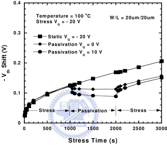
Fig. 2.17 Time dependence of the (a) threshold-voltage shift and (b) threshold- voltage recovery of the devices during the stressing-passivation process………..55 Fig. 2.18 Schematic illustration of the poly-Si/SiO2 interface showing (a) the ≡Si-H defects at the poly-Si/SiO2 interface and in the grain boundaries, (b) generation of the interface trap states, grain-boundary trap states, and fixed oxide charges, and (c) diffusion of the hydrogen species in the gate oxide………..57
Chapter 3
Fig. 3.1 Schematic diagrams illustrating (a) the pulse waveform and (b) the charge- pumping-current curve of a p-channel transistor………69 Fig. 3.2 (a) Schematic cross-sectional view of the critical poly-Si/SiO2 interface showing interface trap states and grain-boundary trap states, and (b) cross-sectional and (c) top views of the LTPS TFT used in this study………70 Fig. 3.3 (a) Charge-pumping current measured with different frequencies, and (b) dependence of the maximum charge-pumping current and the bulk trap-state density on the frequency……….71 Fig. 3.4 (a) Charge-pumping current measured with different pulse amplitudes, and (b) dependence of the maximum charge-pumping current and the bulk trap-state density on the pulse amplitude………...72 Fig. 3.5 Schematic diagrams of the pulse waveform with (a) a small and (b) a large pulse
amplitude. The emission times of both electrons (tem,e) and holes (tem,h) decrease as
the pulse amplitude increases……….73 Fig. 3.6 Schematic diagram illustrating the effect of (a) a large and (b) a small pulse amplitude on the junction region that contributes to the charge-pumping current……….74
Fig. 3.7 (a) Charge-pumping current measured with different rising times, and (b) dependence of the maximum charge-pumping current and the bulk trap-state density on the rising time………...75 Fig. 3.8 (a) Charge-pumping current measured with different falling times, and (b)
dependence of the maximum charge-pumping current and the bulk trap-state density on the falling time………..76 Fig. 3.9 Schematic diagrams of the pulse waveform with (a) a small and (b) a large rising/falling time. The emission times of electrons (tem,e) and holes (tem,h) increase
with the rising time and falling time………..77 Fig. 3.10 (a) Charge-pumping current measured with different source/drain biases, and (b)
dependence of the maximum charge-pumping current and the bulk trap-state density on the source/drain bias……….78 Fig. 3.11 (a) Charge-pumping current measured with different duty ratios, and (b)
dependence of the maximum charge-pumping current and the bulk trap-state density on the duty ratio……….79 Fig. 3.12 Transfer characteristics in the (a) linear and (b) logarithmic scale of the LTPS TFT before and after 1000 s NBTI stress at 150 oC………...80 Fig. 3.13 Charge-pumping current before and after 1000 s NBTI stress under the stress conditions of (a) VG = -15 V at 100 oC, (b) VG = -20 V at 100 oC, and (c) VG
= -15 V at 150 oC………81
Fig. 3.16 Time dependence of the variation of fixed-oxide-charge density under various stress voltages at 100 oC, and dependences the variation of the fixed-oxide-charge density on the (b) stress voltage and (c) stress temperature of the LTPS TFTs under various stress conditions………...86 Fig. 3.17 Comparison of the parameters extracted from the bulk trap-state generation and the fixed-oxide-charge generation………..89 Fig. 3.18 Correlation between the increases of the fixed-oxide-charge density and the threshold-voltage shift………90 Fig. 3.19 Correlation between the increases of the fixed-oxide-charge density and the bulk trap-state density……….91 Fig. 3.20 Energy band diagram of the p-channel LTPS TFT under NBTI stress…………..92
Chapter 4
Fig. 4.1 Process flow of the n-channel LTPS TFT……….102 Fig. 4.2 Antenna geometry of the device structure used in this study. The AR is defined as the antenna area divided by the gate area on the active region………105 Fig. 4.3 Cumulative probability of the threshold voltages for the LTPS TFTs having
various ARs. The threshold voltage was measured at a constant drain current IDS of
10 nA × (W/L) at a value of VDS of 0.1 V……….107
Fig. 4.4 (a) Transfer characteristics and (b) time dependence of the threshold- voltage shift of the LTPS TFTs having various values of AR under a gate-bias stress. Stress condition: VD = VS = 0 V; VG = 30 V……….108
Fig. 4.5 (a) Transfer characteristics and (b) drive-current degradation of the LTPS TFTs having various values of AR under a hot-carrier stress. Stress condition: VGS = 10
Fig. 4.6 Cumulative probability of the threshold voltages for the LTPS TFTs having different channel widths and a fixed AR of 1000……….…………110 Fig. 4.7 Time dependence of the threshold-voltage shift for the LTPS TFTs having different channel widths and a fixed AR of 1000 under a gate-bias stress. Stress condition: VD = VS = 0 V; VG = 30 V……….111
Fig. 4.8 Time dependence of the threshold-voltage shifts for the LTPS TFTs having various channel widths and a fixed AR of 1000 under a hot-carrier stress………...112 Fig. 4.9 Output characteristics of the LTPS TFTs having different channel widths and a fixed AR of 1000 prior to hot-carrier stress. The small circles (Ο) mark the hot-carrier stress conditions used in this study……….113 Fig. 4.10 Transfer characteristics of the LTPS TFTs having channel widths of (a) 5 µm and (b) 30 µm and a fixed AR of 1000 at various hot-carrier stress times………...114
Chapter 5
Fig. 5.1 Schematic cross-sectional diagram of the device structure………..119 Fig. 5.2 Transfer characteristics in the (a) linear and (b) logarithmic scale of the LTPS TFTs with an AR of 100, 500, and 1000 before and after 1000 s NBTI stress…120 Fig. 5.3 Output characteristics of the LTPS TFTs with an AR of (a) 100, (b) 500, and (c)
1000 before and after 1000 s NBTI stress………121 Fig. 5.4 Dependence of the (a) threshold-voltage shift and (b) drive-current degradation on
TFTs with an AR of 100, 500, and 1000 under NBTI stress………128
Chapter 6
Fig. 6.1 Schematic cross-sectional diagram of the LTPS TFT and stress setup. The stress was performed at various stress temperatures with a stress gate voltage (VGS) of
-20 V, and a stress drain voltage (VDS) ranging from 0 to -20 V………137
Fig. 6.2 Transfer characteristics of the LTPS TFTs before and after stress. The stress was performed with a stress gate voltage of -20 V, and stress drain voltages of (a) 0 V and (b) -20 V……….138 Fig. 6.3 Threshold-voltage shift of the LTPS TFTs after various stress conditions. The stress was performed with a fixed stress gate voltage of -20 V, and a stress drain voltage ranging from 0 to -20 V; the temperature was fixed at 25, 75, and 100 o
C………..139 Fig. 6.4 Threshold-voltage shift of the LTPS TFTs after various stress conditions at 100 oC.
The stress was performed with a fixed stress gate voltage of -20 V, and VD = VS
ranging from 0 to -10 V………140 Fig. 6.5 (a) Substrate current of the LTPS TFT measured at 25 and 100 oC under a fixed
stress gate voltage of -20 V, and a stress drain voltage ranging from 0 to -20 V. (b) A simplified sketch of the carrier energy distribution near the drain-end at room temperature and an elevated temperature………141 Fig. 6.6 Schematic diagrams illustrating the vertical-electric field (a) when the stress drain voltage is grounded and (b) when a negative voltage is applied on the drain…..142 Fig. 6.7 Extraction of the parameter C from the fitting of the threshold-voltage shift and the stress voltage………...143 Fig. 6.8 (a) Correlation between the threshold-voltage shift and 1/VDS of the device (W/L =
20µm/20µm) stressed at 25 oC, and (b) comparison of the measured data with the predicted NBTI and HCS effects………..144 Fig. 6.9 (a) Correlation between the threshold-voltage shift and 1/VDS of the device (W/L =
20µm/20µm) stressed at 100 oC, and (b) comparison of the measured data with the predicted NBTI and HCS effects………..145 Fig. 6.10 (a) Correlation between the threshold-voltage shift and 1/VDS of the device (W/L =
20µm/10µm) stressed at 75 oC, and (b) comparison of the measured data with the predicted NBTI and HCS effects……….….146 Fig. 6.11 Degradation of the (a) subthreshold swing (S) and (b) maximum transconductance as a function of the stress drain voltage with a fixed stress gate voltage of -20 V………...147 Fig. 6.12 Degradation of the drive current as a function of the stress drain voltage with a fixed stress gate voltage of -20 V for the devices having a channel length of 20 µm……….148
Chapter 1
Introduction
1.1 Overview of Thin-Film Transistors
Although the concept of a thin-film field-effect transistor was presented as early as 1935 [1.1], the first functional thin-film transistor (TFT) was reported by P. K. Weimer in 1961 [1.2]. Fig. 1.1 shows the cross-sectional and top views of the first TFT in literature, which is composed of a microcrystalline cadmium sulfide (CdS) semiconductor layer, a gate dielectric layer, with gold (Au) source, drain, and gate electrode [1.3]. After that, TFTs have been intensively researched for possible electronic and display applications. The first active-matrix liquid-crystal display (AMLCD) was composed of CdSe TFTs and nematic liquid crystal [1.4]. Although there are many successful demonstrations of CdSe TFT LCDs, the industry did not fly until the report on the feasibility of doping amorphous Si (α-Si) by the glow discharge technique in 1975 was introduced [1.5].
Since then, α-Si TFT LCDs have become the standard for mass-produced AMLCDs for several reasons. First, the characteristics of α-Si TFTs are remarkably well matched to the requirements of liquid-crystal driving, since they have a low OFF current with good ON/OFF ratios. Second, both the gate insulator and the α-Si layers can be deposited in the same plasma-enhanced chemical vapor deposition (PECVD) system, so that contamination of the critical interface can be avoided. Finally, α-Si TFTs can be made at low temperatures (250- 350 oC), thus allowing the use of inexpensive glass substrates [1.6].
However, there are some drawbacks of the α-Si TFTs. The most serious drawback is the low carrier mobility of the α-Si TFT, which is in the range of 0.5-1.0 cm2/Vs. This makes
α-Si TFTs sufficient only for switching devices for each pixel in a display, and cannot meet the desired specifications for high-resolution panels. In addition, the α-Si TFT is not compatible with the CMOS process.
1.1.1 Advantages of Poly-Si TFTs
The problem of the low carrier mobility for the α-Si TFTs can be overcome by introducing polycrystalline silicon (poly-Si) instead of α-Si as a semiconductor layer of TFTs. In addition to a high carrier mobility, there are several advantages of poly-Si TFT LCD. First, the driver circuitry can be integrated on the display’s substrate to realize the system on panel (SOP). Therefore, the size of the total panel and cost, including drivers and related processes, is reduced compared to the α-Si TFT LCDs. Second, the driver contact number of the poly-Si TFT LCD is more than one order of magnitude smaller than that of the α-Si:H TFT LCD. Third, the poly-Si TFT plate has a smaller pixel size and larger aperture ratio in each pixel than that of the α-Si:H TFT plate. Higher mobility means that the pixel charging can be achieved by a smaller-sized TFT, so that it contributes more pixel area for light transmission. Finally, a TFT LCD with self-alignment and CMOS process compatibility can be achieved [1.7], [1.8].
According to the process temperature, there are high-temperature and low-temperature poly-Si TFTs. The process temperatures of low-temperature poly-Si TFTs are as high as 900 oC, thus, expensive quartz substrates are required. Due to the limited profitability of quartz substrate size, most typical applications for high-temperature poly-Si TFT-LCDs are panels
active-matrix liquid-crystal displays (AMLCDs) [1.10]-[1.14], and active-matrix organic light-emitting diode (AMOLED) displays [1.15]-[1.18].
1.1.2 Crystallization of α-Si Thin Films
Among the many barriers to the low-temperature process of LTPS TFTs, the formation of poly-Si films is the most important one. There are several ways to fabricate a low-temperature poly-Si film, described as follows:
(a) Solid-Phase Crystallization (SPC)
Solid-phase crystallization (SPC), focusing on low-temperature annealing, is usually performed at 600 oC [1.19]. The SPC occurs through the processes of nucleation and grain growth, and both processes are characterized by specific activation energies. For the SPC of α-Si by homogenous nucleation, the activation energy of grain growth is less than that of nucleation [1.20]. Therefore, the amount of the nucleation relative to grain growth decreases with decreasing temperature. To enlarge the grain size, it is desirable to minimize the nucleation/grain growth ratio. Therefore, SPC is typically done at a low temperature [1.21]. However, it is time-consuming (several hours) for the crystallization of the α-Si film to a poly-Si film by SPC. Besides, such poly-Si films have a high density of intra-grain defects which result in a decrease in the field-effect mobility and an increase in the threshold voltage of the TFT [1.22].
(b) Metal-Induced Lateral Crystallization (MILC)
With some metals added to the α-Si films, the crystallization temperature can be lowered to below 600 oC, and this phenomenon is known as metal-induced crystallization (MIC) [1.23]. Metals such as Au, Al, Sb, and In, which form eutectics with Si, or metals such as Pd, Ti, and Ni, which form silicides with Si, have been added to α-Si to enhance the
nucleation rate. During the MIC process, metal atoms dissolved in α-Si may weaken Si bonds, and enhance the nucleation of crystalline Si [1.24]. Some results were reported to be successful in lowering the crystallization temperature down to 500 °C. However, an undesirable metal contamination at the channel region results in the poor electrical properties of the devices. A new method which can reduce metal contamination, the so called
metal-induced lateral crystallization (MILC), has been reported for Pd, where large grains
over several tens of microns are obtained [1.25]. Besides, many groups have demonstrated TFTs to be successful in terms of device characteristics and mass productivity with MILC poly-Si, using pure Ni [1.26], [1.27], Ge [1.28] and Ni-Co alloys [1.29].
(c) Excimer Laser Annealing (ELA)
Excimer laser annealing (ELA) is thought to be the most preferable method for the fabrication of LTPS TFTs [1.30]-[1.32]. The ELA method is performed by melting α-Si with high-power pulsed laser irradiation. The irradiated α-Si film is then cooled and solidified as a crystal. During the melt-growth period, however, the solidification velocity is too high for the film to form nuclei and to grow sufficiently. The grain size of the poly-Si film is therefore not large enough. Besides, non-uniformity of grain size and narrow process window make it difficult to achieve uniform TFT performance.
To realize this, some techniques such as the bridge method [1.33], low-temperature substrate heating during laser irradiation [1.34], and two-step laser crystallization [1.35] have been proposed to reduce the solidification velocity. Additionally, for obtaining higher
1.2 Reliability Issues in LTPS TFTs
Research has shown that the instability of LTPS TFTs is more serious after electrical stress than that of single crystalline silicon metal-oxide-semiconductor field-effect transistors (MOSFETs) [1.37]-[1.39]. The poor stability of LTPS TFTs is due to the high density of grain-boundary defects and the poor properties of the poly-Si/SiO2 interface and the gate insulator. A considerable amount of research has focused on the stability of LTPS TFTs. The instabilities are basically associated with hot-carrier degradation, negative gate bias instability, and gate-induced carrier injection [1.40]. In the following, some reliability issues in LTPS TFTs will be roughly reviewed, including negative bias temperature instability, plasma-induced damage, and hot-carrier effects.
1.2.1 Negative Bias Temperature Instability
Negative bias temperature instability (NBTI), which has been known since the 1970s, has been recognized as a serious reliability concern for p-channel MOSFETs, because it can result in the failure of the integrated circuit (IC) [1.37]-[1.43]. Either negative gate voltages or an elevated temperature can produce NBTI, but a stronger and faster effect is produced by their combined action. It occurs primarily in p-channel MOSFETs with negative gate bias stress, but appears to be negligible for positive gate bias stress [1.44]. The NBTI stress is generally performed at an elevated temperature with oxide electric fields typically below 6 MV/cm, and this leads to the degradation of the transistor parameters (drive current, transconductance, and threshold voltage). The low electric fields suppress the carrier injection by Fowler - Nordheim (FN) electron tunneling through a gate oxide, and subsequently there was no direct observable current flow through the oxide [1.45].
In recent years, many fundamental studies have been devoted to NBTI, and it is found that the defects responsible for NBTI are either interface trap states or fixed oxide charges
[1.45]-[1.53]. It is believed that the interface defects responsible for NBTI are Pb centers,
which are depassivated when the negative bias is applied. Fixed oxide charges are created in the SiO2 as by-product trivalent silicon defects [1.45], [1.50]. The amount of generated interface trap states and fixed oxide charges are strongly dependent on fabrication processes such as oxidation and/or annealing. However, this charge-buildup phenomenon is reported to be universal, irrespective of the gate materials, such as Al or polycrystalline silicon, for all wet or dry oxide layers of the Si-SiO2 system [1.45].
Interface traps at the SiO2/Si interface are electrically active defects with an energy distribution throughout the Si band gap. They are acceptor-like in the upper half and donor-like in the lower half of the band gap [1.54]. Interface traps act as generation/recombination centers and contribute to leakage current and low-frequency noise; in addition, they reduce carrier mobility, drain current, and transconductance. Since electrons or holes occupy interface states, they also contribute to threshold-voltage shifts.
However, interfaces traps affect threshold-voltage shifts in n-channel and p-channel devices differently. Fig. 1.2 shows the energy band diagrams of an (a) p substrate and an (b)
n substrate at flatband and inversion conditions. At flatband conditions, the n channel has positive and the p channel has negative interface trap charges (Qit). At inversion conditions,
the n channel has negative and the p channel has positive interface trap charges. Since the fixed oxide charges (Qf) are positive, we have at inversion: Qf - Qit for the n channel and Qf + Qit for the p channel. Therefore, p-channel MOSFETs are more severely affected by
Si3≡Si-H (interface) + ≡Si-O-Si≡ (gate oxide)
Si3≡Si․(interface trap state)+O3≡Si+(fixed oxide charge)+O3≡Si-OH + e-, (Eq. 1.1) where Si3≡Si-H indicates a hydrogenated trivalent silicon, and O3≡Si+ is a trivalent
silicon defect in the oxide. They assume that the silicon interface contains a large number of defects which are electrically inactive, but may become electrically active upon stress. When the defect is activated, the hydrogen, which is weakly bonded to the Si atom, reacts with the SiO2 and forms an OH group bonded to an oxide silicon atom, leaving one trivalent O3≡Si+
in the oxide and one trivalent Si3≡Si․ at the silicon surface. The O3≡Si+
forms the fixed positive charge and the Si3≡Si․ forms the interface trap state. The essence of the diffusion-controlled electrochemical reaction model is that the rate at which the reaction causing the generation of interface trap states takes place is controlled by the diffusion of hydrogen that has been previously released from hydrogen-passivated defect sites. The reaction is schematically represented in Fig. 1.3.
Although the diffusion-controlled electrochemical reaction is generally accepted, there still remains some controversy and debate about the chemical species involved in this dissociation reaction. Some possible diffusing species have been proposed, such as interstitial atomic hydrogen[1.57] - [1.64], molecular hydrogen[1.65] - [1.67], and the hydroxyl (OH) group [1.68], including the hydronium (H3O+) and the dydroxide (OH-) ions. Furthermore, the involvement of ionic hydrogen transport in the reaction has been proposed [1.69]. To generalize the original diffusion-reaction concept to include the charged-diffusing species as well as the neutral-diffusing ones, Ogawa et al. proposed a generalized model which ignores details of the dissociation reaction [1.45], [1.46]. The model is constructed based on the trivalent silicon and its hydrogen compounds to explain the interfacial charge formation. They denote the diffusing state of released hydrogen by the symbol X (i.e., whether it is atomic or molecular/ionic or neutral). The reaction can be expressed as:
(interface defects) (fixed oxide charge)+
+ (interface trap state)
+ Xinterface + e- (to the silicon), (Eq. 1.2)
and
Xinterface Xbulk. (Eq. 1.3)
When the interface defect is electrically activated, the diffusing species leaves a defect site at the Si-SiO2 interface where an interface trap state and a positive fixed oxide charge are left. This model agrees with observations that equal numbers of interface trap states and fixed oxide charges are produced. The process has been considered as being both field dependent, since a transfer of charge takes place, and diffusion controlled, since the time dependence of such a process was found to be characterized by the fractional power-law temporal variation.
In addition to single crystalline silicon MOSFETs, some studies investigated the effects of bias temperature stress on amorphous silicon (α-Si) TFTs. Charge-trapping models [1.70] -[1.72] and meta-stable state creation models [1.73], [1.74] were proposed for positive and negative bias temperature stress. Charge-trapping models attributed the threshold-voltage shift to charge trapping into trap states in the gate insulator from the α-Si layer. Meta-stable state creation models interpreted the threshold-voltage shift as the increase of Si dangling bonds generated by breaking of weak-bonds in α-Si active layers. Meta-stable state creation models have interpreted the threshold-voltage shift as an increase of Si dangling-bonds generated by the breaking of weak-bonds in α-Si active layers. NBTI was also studied in
channels, the grain boundary in the poly-Si channel of TFTs plays an important role in the NBTI-degradation mechanism.
1.2.2 Plasma-Induced Damage
Plasma is a collection of charged and uncharged particles. Positively charged particles are ions; negatively charged particles are either electrons, negative ions or both. Electrons are light and mobile while ions are heavy and comparatively immobile. Plasma is quasi-neutral because it contains equal amount of positive and negative charges. In addition, plasma is not a system at thermal equilibrium; however, it is at a steady state very far from equilibrium.
In the fabrication of VLSI devices and circuitry, plasma processing is widely applied for material etching. Etching can be accomplished by physically displacing atoms or molecules, and this mechanism is called physical sputtering. In this process, ion bombardment can cause breakage of chemical bonds and damage to the dielectric and semiconductor materials. Alternatively, a chemical reaction can also be used to form a volatile product of the atoms or molecules to be removed, and this process is called chemical etching. In chemical etching, the plasma creates a reactive etchant species such as radicals or neutrals, and reactant species are produced through dissociation and reaction. Table 1.1 summarizes the various types of damage to the materials involved in semiconductor fabrication [1.78]. During the plasma etching process, plasma-induced damage affects the material properties and device parameters. One of the damages caused by plasma is charging damage, which is becoming a serious reliability problem for device fabrication and has been reported to cause degradation to the hot-carrier lifetime, transistor performance, and gate oxide quality [1.79]-[1.83].
The nature of charging damage in the gate oxide of a transistor is similar to that of FN stress. In the plasma ambient, plasma non-uniformities cause a charge collection by conducting layers such as metal or poly-Si electrodes [1.84]. If the conducting layer is
connected to the gate oxide, the collected charges cause an electrical stress on the gate oxide. When the non-uniformity is large enough and the potential across the gate oxide exceeds the critical value (corresponding to a field of 5-6 MV/cm), an FN tunneling current flows through the gate oxide. During plasma processing, the injection process could be either substrate injection or gate injection depending on potential distribution at the wafer surface [1.85]. Several processes responsible for oxide and transistor degradation take place simultaneously during the FN current flow. First, some of the injected electrons are trapped in existing electron traps. At the same time, holes generated by injected hot electrons are trapped in existing hole traps. Additionally, interface states are generated, resulting in a high density of interface states. Finally, new electron traps are generated, and fill in the oxide bulk. All of these phenomena occur during the charging stress due to plasma exposure of the conducting layers [1.86]. The net result is an accumulation of a net charge in the oxide, and hence it is referred to as the oxide charging effect. The charging effect additionally is found to be amplified by the ratio of the area of the conducting surface to the gate area, and this ratio is called the antenna area ratio (AR). This phenomenon is referred as the antenna effect. It is therefore customary to use a device with different antenna structures to study charging damage. For LTPS TFTs, because they have a high potential to be used in the driving circuit, the antenna structure will be very common in the circuit layout, and the antenna effect becomes an important reliability issue.
high drain field has been widely studied in many articles [1.87]-[1.89]. Carriers obtain energy from a high electric field and break weak bonds easily, creating lots of oxide charges and trap states in the channel film and at poly-Si/SiO2 interface. Hot-carrier stress degrades devices by decreasing the maximum transconductance and causing a variation of the threshold voltage. In addition, the power dissipation increases and the reliability of digital circuit degrades. Therefore, the hot-carrier effect restricts the design of flat-panel displays.
In LTPS TFTFs, unlike the fundamental MOSFETs theory, electrical parameters such as the threshold voltage, maximum transconductance, and subthreshold swing could depend on the properties of grain, grain boundaries, and poly-Si/SiO2 interface. Farmakis et al. have investigated electrical parameters in TFTs, as shown in Table 1.2, to clarify which mechanisms modify device electrical parameters during hot-carrier stress [1.90]. The deep trap states in the grain boundaries or poly-Si/SiO2 interface mainly affect the threshold voltage. In addition, hot-carrier injection into the gate oxide also causes a threshold-voltage shift. The generations of tail trap states in the grain boundaries or poly-Si/SiO2 interface degrades the maximum transconductance. Furthermore, the subthreshold swing mainly depends on both intra-grain trap states in the poly-Si film and deep interface trap states.
1.3 Motivation
Since the reliability of LTPS TFTs is important for the application of high-performance displays with integrated circuits, the degradation mechanism of LTPS TFTs must be investigated carefully. For driving circuit operation, LTPS TFTs must be designed using the CMOS inverter configuration and operate with a relatively high duty cycle. Therefore, NBTI becomes a reliability issue for p-channel LTPS TFTs since they are subjected to negative bias stress during circuit operation. In LTPS TFTs, because of the poor thermal conductivity of the glass substrate and high operation voltage, NBTI can be further accelerated because it
can be thermally and electrically accelerated. Besides, due to the grain boundaries in the channel regions, the NBTI-degradation mechanism of LTPS TFTs may be different from that of MOSFETs. However, the NBTI degradation has not been thoroughly studied in LTPS TFTs, and the mechanism is not well known. Therefore, in Chapter 2, the NBTI-degradation mechanism of p-channel LTPS TFTs will be studied.
It is important to investigate the degradation of the bulk channel region in LTPS TFTs under NBTI stress because the characteristics of LTPS TFTs are generally influenced by the bulk trap states (including grain-boundary and poly-Si/SiO2 interface trap states). In traditional studies, the bulk trap-state evaluation methods were based on the current-voltage characteristics. However, the channel current is affected only through the potential barrier formed by the trap states and hence is not directly related to the bulk trap properties. To directly characterize the bulk trap properties of LTPS TFTs, a charge-pumping technique will be used in Chapter 3, because carriers are observed as the generation-recombination current, and hence the charge-pumping current directly indicates the trap properties. Besides, in previous NBTI studies of LTPS TFTs, the correlation between the fixed-oxide-charge generation and NBTI degradation has not been clearly identified. Therefore, the role of fixed-oxide-charge generation will also be analyzed in Chapter 3.
In addition to the NBTI degradation, plasma-induced damage is an important reliability issue for LTPS TFTs, because plasma-etching processes are widely adopted during the fabrication procedure to achieve good process repeatability and precise control over the feature sizes in the insulators, semiconductors, and metals. Plasma non-uniformity causes
performance and reliability of LTPS TFTs have not been explored to an appropriate degree. Therefore, in Chapter 4, n-channel LTPS TFTs designed with various antenna structures will be used to investigate the impacts of the antenna effect.
Both the NBTI and the antenna effect are serious reliability issues for LTPS TFTs. An antenna effect mainly occurs during the fabrication process and degrades the oxide quality, while NBTI primarily occurs during circuit operation and degrades the performance. Pagaduan et al. have pointed out that devices suffering plasma damage exhibit an aggravated threshold-voltage shift after NBTI stress [1.91]. However, the correlation between the antenna effect and NBTI in LTPS TFTs has not been explored. Therefore, in Chapter 5, effects of NBTI stress will be analyzed on p-channel LTPS TFTs designed with various antenna structures to verify the impact of the antenna effect on the NBTI behaviors in LTPS TFTs.
Hot-carrier effects, which originate from the high electric field near the drain junction, have been commonly used for reliability assurance, and widely studied in LTPS TFTs. Because the LTPS TFT driving circuit is designed using the CMOSFET structure, hot-carrier stress (HCS) becomes a transient phenomenon that mixes with the effect of NBTI. However, the mixed effects of NBTI and HCS are rarely explored for LTPS TFTs. Therefore, in Chapter 6, the combined effect of NBTI and HCS will be investigated, in which the LTPS TFTs will be stressed with a fixed gate bias and variable drain bias to identify the drain bias dependence of the threshold voltage shift.
1.4 Thesis Organization
This thesis is organized as follow:
In Chapter 1, the overview of LTPS TFTs and some reliability issues are illustrated. The motivation of this thesis is also described.
In Chapter 2, NBTI of p-channel LTPS TFTs is thoroughly studied. In addition to the threshold-voltage shift, the generation of grain-boundary trap states and interface trap states are analyzed. A stressing-passivation-stressing procedure is also used to study the effect of threshold-voltage recovery. From the experimental results, the NBTI-degradation mechanism of LTPS TFTs is identified.
In Chapter 3, a charge-pumping technique is utilized to analyze the NBTI degradation of LTPS TFTs. In addition to the increase of bulk trap states (including interface and grain-boundary trap states), the increase of fixed oxide charges is also extracted. By using this technique, the NBTI-degradation mechanism of LTPS TFTs can be further confirmed
In Chapter 4, n-channel LTPS TFTs designed with different antenna area ratios are used to study the impacts of an antenna effect on the device performance and reliability. Electrical characteristics of the devices were measured to identify the influence of the antenna effect. Finally, gate-bias stress and hot-carrier stress were used to analyze the degradation of device reliability.
In Chapter 5, the impacts of the antenna effect on the NBTI behaviors are investigated. NBTI stress was performed on the LTPS TFTs having different antenna area ratios. By extracting the related device parameters, the antenna effect can be demonstrated to enhance the NBTI degradation in LTPS TFTs.
In Chapter 6, a reliability model is proposed which successfully introduces the physical mechanisms of both the NBTI and HCS for p-channel LTPS TFTs. The stress drain bias voltage is introduced into the conventional NBTI degradation model to develop a
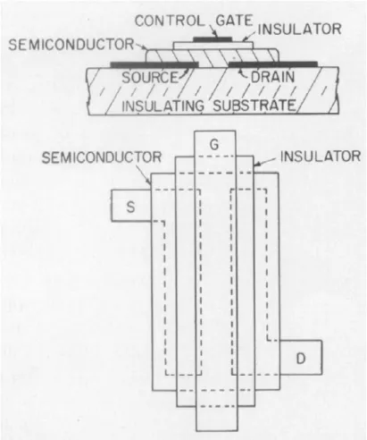
Fig. 1.1 Cross-sectional and top views of the first TFT in literature. (Ref. Weimer, IRE-AICE Device Research Conference, 1961)
Fig. 1.2 Energy band diagrams of the Si substrate showing the occupancy of interface traps and the various charge polarities: an (a) p-type substrate with positive interface trap charges at flatband condition and negative interface trap charges at inversion
Fig. 1.3 Schematic two-dimensional representation of the Si-SiO2 interface, showing (a) the Si3≡Si-H defect, and (b) how this defect may be electrically activated during NBTI stress to form a surface trap , an oxide charge, and a hydroxyl group, that (c) may diffuse in the oxide and be the reaction-limiting factor.
(Ref. Jeppson and Svensson, J. Appl. Phys., 1977)
Si
3≡
≡
≡
≡Si-
-
-
-H defect
Si
3≡
≡Si
≡
≡
․ ․ ․ ․+
+
+
+O
3≡
≡
≡
≡Si
+ + + ++
+
+
+≡
≡
≡
≡Si-
-
-OH
-
Diffusing OH-group
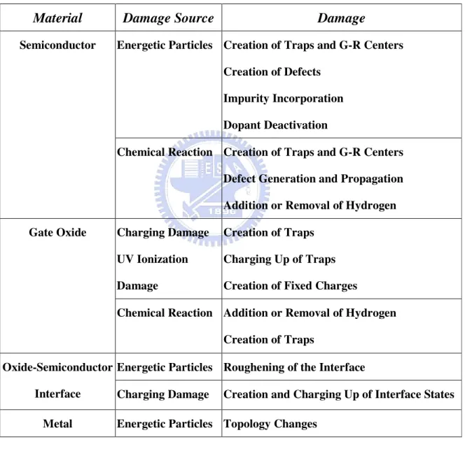
Table 1.1 Various types of material damage involved in the semiconductor fabrication. (Ref. Rakkhit et al., in Proc. IEEE Int. Reliab. Phys. Symp., 1993.)
Material
Damage Source
Damage
Energetic Particles Creation of Traps and G-R Centers Creation of Defects
Impurity Incorporation Dopant Deactivation Semiconductor
Chemical Reaction Creation of Traps and G-R Centers Defect Generation and Propagation Addition or Removal of Hydrogen Charging Damage
UV Ionization Damage
Creation of Traps Charging Up of Traps Creation of Fixed Charges Gate Oxide
Chemical Reaction Addition or Removal of Hydrogen Creation of Traps
Energetic Particles Roughening of the Interface Oxide-Semiconductor
Table 1.2 Parameter variations and corresponding possible degradation mechanics. (Ref. Farmakis et al., IEEE Electron Device Lett., 2001.)
Chapter 2
Negative Bias Temperature Instability in
Low-Temperature Polycrystalline Silicon
Thin-Film Transistors
2.1 Introduction
LTPS TFTs are attracting much research interest for their various applications, such as driver circuits of active matrix liquid crystal displays (AM-LCDs) and active matrix organic light emitting diode displays (AM-OLED). Moreover, due to the high carrier mobility of LTPS TFTs, they have high potential of realizing system on panel (SOP), in which the peripheral drivers can be integrated on the glass substrates to minimize the panel size, improve the reliability and resolution of the displays, yield a light and thin display having a reduced number of connection pins, and reduce the fabrication cost [2.1], [2.2]. For the driving circuit operation, LTPS TFTs must be designed using the CMOS inverter configuration. Unlike the functionality for pixel switching, the peripheral driving circuits operate with a relatively high duty cycle. Accordingly, the p-channel and n-channel TFTs are subjected to negative and positive bias stress, respectively. Fig. 2.1 gives a more detailed picture of the correlated information. It presents the bias conditions of a CMOS inverter for
In p-channel MOSFETs, NBTI has been found to be an important reliability problem which has been widely investigated. The NBTI-degradation in MOSFETs is mainly attributed to the generation of interface trap states and fixed oxide charges, and it can be thermally and electrically activated [2.4]-[2.7]. Besides, it is accepted that degradation partially recovers once stress is removed [2.8], [2.9]. The recovery of the NBTI degradation comes from the reduction of interface trap states and fixed oxide charges. In LTPS TFTs, due to the poor thermal conductivity of the glass substrate and high operation voltage, we suppose that NBTI is important to the reliability of LTPS TFTs. Okuyama et al. have pointed out that the NBTI stress causes a performance degradation in poly-Si TFTs as well as in MOSFETs [2.10], [2.11]. However, the NBTI degradation and the recovery effect have not been thoroughly studied in LTPS TFTs, and the mechanisms are not well known. In addition, we speculate that the NBTI-degradation mechanism in LTPS TFTs, due to grain boundaries in the channel regions, may be different from those in MOSFETs. Some studies have indicated that the NBTI stress on poly-Si TFTs may generate trap states in the grain boundaries [2.11]; however, the correlation between the grain-boundary trap-state generation and the device degradation during NBTI stress in LTPS TFTs has not been well explored.
In this chapter, the instability and mechanism of p-channel LTPS TFTs under NBTI stress have been studied. Positive bias temperature instability (PBTI) is also measured to be compared with the NBTI effect. By measuring and analyzing the transfer and output characteristics before and after NBTI stress under different stress gate voltages and stress temperatures, the NBTI degradation and recovery mechanisms of LTPS TFTs were studied and a new model is proposed to explain the experimental results.
2.2 Experiments
flow of the p-channel LTPS TFT is shown in Figs. 2.2(a) - 2.2(g). First, a 400-Å amorphous-Si layer was deposited by a plasma-enhanced chemical-vapor deposition (PECVD) system on a buffer layer and crystallized into a poly-Si film through excimer laser annealing. After defining the active region, the gate dielectric of the 1000-Å SiO2 layer was deposited at 300 oC. Mo was then deposited at a thickness of 3000 Å and patterned as the gate electrode. Self-aligned source and drain were formed through plasma doping. Following that, hydrogenation was performed with an NH3 plasma treatment at 300 oC to passivate the dangling bonds at the poly-Si/SiO2 interface and in the grain boundaries. A 5000-Å inter-layer dielectric of SiO2 was then deposited and densified through rapid thermal annealing (RTA) at 700 oC for 30 s. The dopants were activated during the densification of the inter-layer dielectric. Finally, after a contact-hole opening, 5000-Å Al was deposited and patterned as the interconnection metal. The channel length (L) and width (W) of the device used in this study were 10 µm and 20 µm, respectively.
During stress, the glass substrate was heated to stress temperatures ranging from 25 oC to 150 oC. Stress gate biases were +15 V as PBTI stress, and ranging from -15 to -30 V as NBTI stress. Source and drain were electrically grounded. The stress was periodically stopped to measure the basic device characteristics, including transfer and output characteristics, to characterize the NBTI effect. All the measurements were taken at stress temperatures.
indicates that PBTI is an important issue for p-channel LTPS TFTs. Besides, during inverter operation, p-channel LTPS TFTs will be subjected to NBTI stress instead of PBTI stress. Therefore, only NBTI degradation will be discussed below.
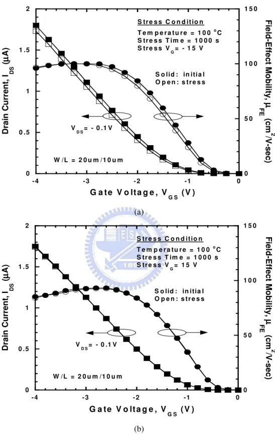
2.3.1 Device Degradation Due to NBTI
Figs. 2.4(a) and 2.4(b) show the transfer characteristics and output characteristics of the LTPS TFT under NBTI stress, respectively. The stress was performed at 100 oC with a stress gate voltage of -30 V for 1000 s. In Fig. 2.4(a), it is observed that the threshold voltage shifts to the negative direction after the NBTI stress. In addition, the NBTI stress also leads to the performance degradation in the subthreshold swing, field-effect mobility, and drive current. The degradation of the subthreshold swing and field-effect mobility is attributed to the interface-trap-state generation. The drive current of LTPS TFTs can be given in the simple form: DS th GS ox FE ON
V
V
V
L
W
C
I
=
µ
(
−
)
. (Eq. 2.1) The two parameters leading to the degradation of the drive current (ION) are thethreshold-voltage (Vth) shift and field-effect mobility (µFE) decrease. Therefore, the reduction
of the drive current after NBTI stress can be attributed to the threshold-voltage shift and field-effect mobility degradation. Furthermore, the leakage current also increases after stress which leads to the increase of standby current.
In MOSFETs, the threshold-voltage shift caused by the NBTI stress is generally attributed to the generation of fixed oxide charges and interface trap states [2.4]-[2.7]. In poly-Si TFTs, however, there are many grain boundaries in the channel regions, and the grain boundaries may be degraded under NBTI stress. Therefore, in addition to the generation of fixed oxide charges and interface trap states, we suggest that the threshold-voltage shift in poly-Si TFTs is also attributed to the grain-boundary trap-state creation. The detailed
analysis of the correlation between the grain-boundary trap-state generation and the threshold-voltage shift under NBTI stress will be discussed in the latter section.
2.3.2 Analysis of the Threshold-Voltage Shift
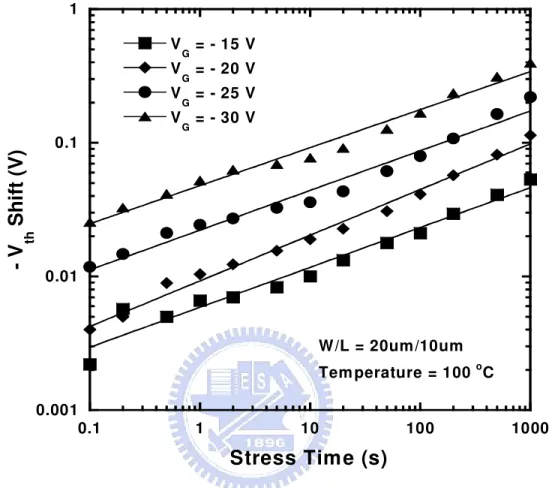
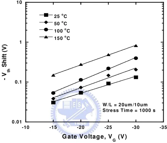
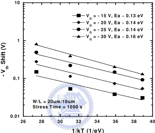
Figs. 2.5(a)-2.5(c) show the dependence of the threshold-voltage shift on the stress time, stress voltage, and stress temperature, respectively. The gate voltage at a specified threshold drain-current (IDS), (W/L) × 10 nA for VDS = -0.1 V, is taken as the threshold
voltage. In Fig. 2.5(a), the threshold-voltage shift increases upon increasing the stress time, and it shows a power law dependence on the stress time. It is observed that the threshold-voltage shift slightly fluctuates as a function of the stress time; this is because the magnitude of the threshold-voltage shift under NBTI stress is very small (< 0.1 V for short stress time). Actually, the correlation coefficients of the four fitting curves in Fig. 2.5(a) are all above 0.98, which means that the measured data and the fitting curves almost fit together. In Figs. 2.5(b) and 2.5(c), it is found that the NBTI degradation is enhanced at a higher stress voltage or stress temperature, indicating that the NBTI can be electrically and thermally activated.
The behavior of the threshold-voltage shift can be empirically modeled as [2.12]
G a kT CV E n th
t
e
e
V
∝
(− / )∆
, (Eq. 2.2) where the exponent n approximates from 0.28 to 0.34 in our experimental results, which is similar to the results previously reported for poly-Si TFTs [2.10], [2.11], and bulk MOSFETsNBTI-degradation mechanism is related to the ionic drift, as shown in Fig. 2.6(a), the threshold voltage should shift to the positive direction, however, this clashed with the experimental results. On the other hand, in some models of charge trapping in gate dielectric [2.14], it is revealed that when the device is under gate bias stress, charges may inject into the gate dielectric and generate extra trap states, leading to the threshold-voltage shift, as shown in Fig. 2.6(b). In our experiments, there are several reasons to explain why the device degradation under NBTI stress was not due to the charge trapping in the gate dielectric. First, if the threshold-voltage shift is caused by the electron injection from the gate into the gate dielectric, the threshold voltage should shift to the positive direction. However, this clashed with the experimental results. Second, if the degradation is caused by the hole injection from the channel to the gate dielectric, the threshold voltage will shift to the positive direction. This seems consistent with the experimental results. However, the electric field across the gate dielectric (below 3 MV/cm) was not high enough to cause hole injection, and the Fowler -Nordheim current was undetectable at these bias conditions, as shown in Fig. 2.7. Therefore, the extra trap-state generation and device instability caused by small currents can be neglected [2.16]. Third,previous studies showed that the threshold-voltage shift caused by the charge-trapping process exhibits exponential dependence on 1/VG and is virtually temperature independent [2.14], [2.15]. If the threshold-voltage shift is caused by charge trapping, it should have the same dependence on the stress gate voltage and stress temperature as in the charge-trapping model. However, the charge-trapping model can’t explain the exponential dependence of the threshold-voltage shift on VGand 1/T as shown in
Figs. 2.5(b) and 2.5(c), respectively. Finally, the charge-trapping models [2.14] cannot explain the linear fit of the log-log plot of the threshold-voltage shift versus the stress time as shown in Fig. 2.5(a). Therefore, instead of ionic drift or charge trapping in the gate dielectric, we suggest that the threshold-voltage shift caused by NBTI stress is due to the charge defect creation in the gate oxide, and trap-state generation at the poly-Si/SiO2 interface and in the