國立交通大學
電信工程學系
碩士論文
應用於超寬頻與 802.11a 無線射頻接收機之
CMOS 低功率低電壓及改善閃爍雜訊技術之混
頻器與超低功率混頻器之設計與研究
Design of CMOS Low Power Low Voltage Mixer with Flicker
Noise Improved Technique and Ultra Low Power Mixer for
UWB and 802.11a Wireless RF Receiver
研究生:陳志豪
指導教授:周復芳 博士
應用於超寬頻與
802.11a 無線射頻接收機之 CMOS 低功率低電壓
及改善閃爍雜訊技術之混頻器與超低功率混頻器之設計與研究
Design of CMOS Low Power Low Voltage Mixer with Flicker Noise
Improved Technique and Ultra Low Power Mixer for UWB and
802.11a Wireless RF Receiver
研究生:陳志豪 Student: Chih Hao Chen
指導教授:周復芳 博士 Advisor: Dr. Christina F. Jou
國 立 交 通 大 學
電 信 工 程 學 系 碩 士 班
碩 士 論 文
A thesis
Submitted to Department of Communication Engineering College of Electrical and Computer Engineering
National Chiao Tung University In Partial Fulfillment of the Requirements
for the Degree of Master of Science in Communication Engineering
June 2008
Hsinchu, Taiwan, Republic of China
中華民國九十七年六月
I
應用於超寬頻與
802.11a 無線射頻接收機之 CMOS 低功率低電壓
及改善閃爍雜訊技術之混頻器與超低功率混頻器之設計與研究
研究生:陳志豪 指導教授:周復芳 博士
國立交通大學電信工程學系碩士班
摘 要
本論文探討應用於超寬頻與 802.11a 機收機的高頻混頻器之設計,其中分成兩個 主題來探討。第一主題是混頻器之低功率低電壓以及改善閃爍雜訊之設計與分析。首 先設計應用在超寬頻系統之低電壓低功率混頻器,利用 PMOS 與 NMOS 折疊式轉導 級混頻器來達到低電壓的效果,再利用電容來各自偏壓來降低供應電壓,此供應電壓 為1V。量測結果顯示,在供應電壓 1V 下,混頻器僅消耗 2.9 毫瓦,並且擁有 3.1~10.6 GHz 的頻寬,並且轉換增益在 3.1~9.6 GHz 中僅 1 dB 之變動,達到既平坦又寬頻之低 功率低電壓混頻器。針對上述混頻器發現,應用在直接降頻混頻器下閃爍雜訊影響甚 大,所以接著探討閃爍雜訊在混頻器中扮演的腳色。進一步將改善閃爍雜訊的技巧應 用在上述混頻器中,量測結果顯示,在5.2 GHz (802.11a) 工作頻率下雜訊指數降低 4 dB 且轉換增益提升 4.8 dB。 第二主題為超低功率混頻器之實現。模擬結果顯示在供應電壓為 0.6V 下,功率 僅消耗0.57 毫瓦,但增益為 1.7 dB,雜訊指數為 11.25 dB。經過適當的修改之後,一 樣在0.6V 供應電壓下,功率消耗 0.42 毫瓦,並且擁有 5.2 dB 之增益且雜訊指數為 9.5 dB。 最後對於閃爍雜訊在混頻器中的影響提出新解決方案,電路架構也已完成初步構 想,將作為此論文將來專題之研究。II
Design of CMOS Low Power Low Voltage Mixer with Flicker Noise
Improved Technique and Ultra Low Power Mixer for UWB and
802.11a Wireless RF Receiver
Student: Chih Hao Chen Advisor: Dr. Christina F. Jou
Department of Communication Engineering
National Chiao Tung University
ABSTRACT
This thesis discusses high frequency mixer for UWB and 802.11a receivers and it mainly includes two parts. One is the analysis and design of low power low voltage mixer with flicker noise improved technique. First, the low power and low voltage mixer which utilizes folded transconductance stage including PMOS stacked on the top of NMOS is implemented for UWB system. Then the capacitor is used for NMOS and PMOS biasing by oneself to implement low supply voltage with 1V. The measured results reveal that this mixer consumes only 2.9 mW with 1V supply voltage and its bandwidth is 3.1~10.6 GHz. In 3.1~9.6 GHz, the variation of conversion gain is only 1 dB and the mixer achieves flat gain and broadband performance. In described above, flicker noise is strongly influenced and play an important role in direct conversion receivers. Flicker noise improved technique is adopted in above mixer. The measured results reveal noise figure is reduced 4 dB and conversion gain is increased 4.8 dB at 5.2 GHz (802.11a).
In part two, the Ultra low power mixer is implemented. The simulated results reveal power consumption is only 0.57 mW, conversion gain is 1.7 dB, and noise figure is 11.25
III
dB with 0.6V supply voltage. After moderate modifying, power consumption is 0.42 mW, conversion gain is 5.2 dB, and noise figure is 9.5 dB.
At the last, we propose the solution to solve the influence in mixers. The construct is completed and is treated as future work in our thesis.
IV
誌謝
研究所兩年的生活,首先我要感謝周復芳博士細心指導,讓我在射頻積體電路領 域中獲益良多,並且培養了正確的研究態度與精神,以及解決問題的能力。同時要感 謝郭建男博士及胡樹博士對於論文的不吝指導,寶貴意見與建議使得整體觀念更加 完備,論文更加完善。 感謝實驗室的博班學長匯儀、俊緯、智鵬、宜星等的指導,同學沛遠、智元、昭 竹、昱舜、廉昇的指教,以及學弟昭維、子哲、玠瑝、奕霖、宗廷的幫忙,讓碩士兩 年來多采多姿。另外要感謝已畢業的學長子豪,對於專業領域方面的指導,還要感謝 小碰在碩士生涯的陪伴,讓我充滿動力努力研究。 最後要感謝我的爹娘與兄長,在我求學生涯中尊重我的選擇與支持我的決定,能 讓我順利碩士畢業。在這裡將我的研究獻給我的親人,沒有你們就沒有現在的我。陳志豪
于 新竹交大
2008 年 夏
V
CONTENTS
Chinese Abstract I
English Abstract II
Acknowledgement IV
Contents V
List of Tables VII
List of Figures VIII
Chapter 1
Introduction ... - 1 -
1.1 Background and motivation ... - 1 -
1.2 Thesis organization ... - 2 -
Chapter 2
Section I
Low Power and Low Voltage UWB Mixer ... - 3 -
I. 2.1 Introduction ... - 3 -
I. 2.2 Low power and low voltage folded mixer ... - 4 -
I. 2.3 Chip implementation and measured consideration ... - 8 -
I. 2.4 Measurement results and discussion ... - 12 -
Chapter 2
Section II
Low Power Mixer with Flicker Noise Improved Technique 25
-II. 2.1 Introduction ... - 25 -II. 2.2 Flicker noise in mixers ... - 25 -
II. 2.3 Low power mixer with flicker noise improved technique ... - 32 -
II. 2.4 Chip implementation and measured considerations ... - 35 -
II. 2.5 Measurement results and discussion ... - 38 -
II. 2.6 Comparison ... - 43 -
-VI
3.1 Introduction ... - 44 -
3.2 Ultra low power mixer ... - 46 -
3.3 Chip implementation and measured considerations ... - 49 -
3.4 Simulation results and discussion ... - 51 -
3.5 Comparison ... - 62 -
Chapter 4
Future Work ... 63
-4.1 Future Work ... - 63 -
-VII
LIST
OF
TABLE
Table 2.1 Simulated and measured performance of the folded low power mixer .... 24
Table 2.2 Simulated and measured performance of the folded low power mixer with improving flicker noise ... 42
Table 2.3 Measured results with and without inductor ...43
Table 3.1 Simulated performance of the Ultra low power mixer ...61
VIII
L
IST
O
F
F
IGURE
Figure 2.1 Down conversion receiver ... 4
Figure 2.2 Proposed UWB low power low voltage mixer ... 4
Figure 2.3 RF matching network ... 5
Figure 2.4 Transconductance stage (a) with resistor stacked on the top of the NMOS (b) with PMOS stacked on the top of the NMOS and bias by oneself ... 6
Figure 2.5 Layout of the proposed UWB low power mixer ... 8
Figure 2.6 Die photograph of the proposed UWB low power mixer ... 8
Figure 2.7 on wafer circuit measurement with PCB bias network ... 9
Figure 2.8 Measurement setup of the proposed UWB low power mixer for (a) input return loss (b) conversion gain and P1dB (c) IIP3 (d) noise figure ... 10
Figure 2.9 (a) (b) The whole measurement environment in CIC ... 11
Figure 2.10 The measured and simulated RF return loss ... 13
Figure 2.11 The measured and simulated IF return loss ... 13
Figure 2.12 The measured and simulated conversion gain versus LO power (a) RF frequency at 3.1 GHz (b) RF frequency at 5.1 GHz (c) RF frequency at 7.1 GHz (d) RF frequency at 9.1 GHz (e) RF frequency at 10.6 GHz ... 14
Figure 2.13 The measured and simulated P1dB (a) RF frequency at 3.1 GHz (b) RF frequency at 4.1 GHz (c) RF frequency at 5.1 GHz (d) RF frequency at 6.1 GHz (e) RF frequency at 7.1 GHz (f) RF frequency at 8.1 GHz (g) RF frequency at 9.1 GHz (h) RF frequency at 10.6 GHz ... 16
Figure 2.14 The measured and simulated conversion gain versus frequenc ... 16
Figure 2.15 The measured and simulated input third order intercept point (IIP3) ... 18
Figure 2.16 The measured and simulated isolation LO_IF versus frequency ... 19
Figure 2.17 The measured and simulated isolation LO_RF versus frequency ... 19
Figure 2.18 The measured and simulated isolation RF_IF versus frequency ... 20
Figure 2.19 The measured and simulated noise figure versus frequency ... 20
Figure 2.20 Simulated gm, gm2, and gm3 characteristic versus gate-to-source voltage (a) NMOS (M1) (b) PMOS (M3) ... 22
Figure 2.21 CMOS input voltage versus output voltage... 23
Figure 2.22 CMOS input voltage versus output voltage with capacitor C ... 23
Figure 2.23 Noise pulses resulting in flicker noise at mixer output ... 26
Figure 2.24 Conventional Gilbert cell with current bleeding ... 28
Figure 2.25 Conventional Gilbert cell with dynamic current bleeding ... 28
Figure 2.26 (a) Dynamic current injection (b) Nodes waveform ... 29
Figure 2.27 Current bleeding technique with inductor ... 30 Figure 2.28 Equivalent model of double-balanced mixer with current bleeding
IX
circuit and one resonating inductor ... 31
Figure 2.29 The proposed low power mixer with low flicker noise ... 32
Figure 2.30 The simulated conversion gain with and without resonant inductor L . 34 Figure 2.31 The simulated noise figure with and without resonant inductor L ... 34
Figure 2.32 Layout of the proposed low power mixer with improving flicker noise ... 35
Figure 2.33 Die photograph of the proposed UWB low power mixer ... 36
Figure 2.34 On wafer circuit measurement ... 36
Figure 2.35 Measurement setup of the proposed folded mixer with improving flicker noise for (a) input return loss (b) conversion gain and P1dB (c) IIP3 (d) noise figure ... 37
Figure 2.36 The simulated RF return loss ... 39
Figure 3.37 The simulated and measured LO Power versus conversion gain ... 39
Figure 2.38 The simulated and measured P1dB ... 40
Figure 2.39 The simulated and measured input third order intercept point (IIP3) ... 40
Figure 2.40 The simulated and measured noise figure versus IF Frequency ... 41
Figure 3.1 Single balance mixer ... 45
Figure 3.2 Complementary current reused mixer ... 45
Figure 3.3 Complementary current reused mixer with current bleeding technology45 Figure 3.4 the proposed Ultra low power mixer ... 46
Figure 3.5 Conversion gain versus Ratio of current bleeding ... 47
Figure 3.6 Noise figure versus Ratio of current bleeding ... 48
Figure 3.7 Layout of the proposed mixer ... 49
Figure 3.8 On wafer measurement for ultra low power Mixer ... 49
Figure 3.9 Measurement setup of the proposed UWB low power mixer for (a) input return loss (b) conversion gain and P1dB (c) IIP3 (d) noise figure ... 51
Figure 3.10 The simulated RF return loss ... 52
Figure 3.11 The simulated LO Power versus conversion gain ... 52
Figure 3.12 The simulated P1dB ... 53
Figure 3.13 The simulated input third order intercept point (IIP3) ... 53
Figure 3.14 The simulated noise figure versus Frequency ... 54
Figure 3.15 (a) Ultra low power mixer with current bleeding R (b) Ultra low power mixer with current bleeding M2 ... 55
Figure 3.16 The simulated conversion gain versus LO power ... 56
Figure 3.17 The simulated RF and IF return loss ... 57
Figure 3.18 The simulated P1dB at 5.2 GHz ... 57
Figure 3.19 The simulated IIP3 at 5.2 GHz ... 58
X
Figure 3.21 The simulated isolation (a) LO to IF isolation (b) LO to RF isolation
(c) RF to IF isolation ... 59
Figure 3.22 layout of the proposed mixer ... 60
Figure 3.23 Differential in single out output buffer ... 60
Figure 4.1 Conventional Gilbert cell mixer ... 64
Figure 4.2 Dynamic current bleeding with resonant inductor ... 64
Figure 4.3 Equivalent circuit of resonant inductor ... 65
Figure 4.4 The proposed mixer to reduce flicker noise ... 66
Figure 4.5 The equivalent model of double balance mixer with current bleeding circuit and two resonating inductors ... 67
- 1 -
Chapter 1
Introduction
1.1 Background and motivation
With the development of science and technology, a large number of communicated products which include mobile phone, GPS, Bluetooth, and wireless local area network (WLAN) are presented to satisfy people’s demand. Due to the progress of integrated circuit technique, communicated equipment is more and more diversified. For different area, different specification is developed. Each system for data transmission, modulation, bandwidths has different demands. For many different requirements, the designers should have different field knowledge just like RF system, microwave engineering, impedance matching, inter-stage matching network, and understanding of the parameter. The balance between parameters like gain, noise, and linearity is the relation of trade-off. The designer should know well to achieve the optimum for the specification. In this thesis, circuits are designed for UWB and 802.11a system.
In 2002, the Federal Communications Commission (FCC) has allocated 7500-MHz bandwidth for ultra-wideband (UWB) applications in the 3.1–10.6 GHz frequency range [1] [2]. UWB is a radio frequency. It is defined as any signal whose fractional bandwidth is equal to or greater than 20% of the center frequency or that occupies a bandwidth equal to or greater than 500MHz. The large occupied bandwidth (7500MHz) provides high data rates up to several hundred Mbps. A difference between traditional and UWB radio transmission is that traditional systems transmit signal by modulate the power, frequency, and phase. UWB systems transmit signal by generating energy and occupying broad bandwidth for time modulation. The
- 2 -
power spectral density emission limit in the UWB band is -43 dBm/MHz.
In 1997, IEEE 802.11 is defined. In 1999, 802.11a is defined at 5 GHz for ISM band. The 802.11a standard has three U-NII (Unlicensed National Information infrastructure) bands. They includes the lower band (5.15-GHz ~ 5.25-GHz), the middle band (5.25-GHz ~ 5.35-GHz) and the upper band (5.725-GHz ~ 5.825GHz). The lower and middle sub-bands have rooms for eight channels in the total bandwidth of 200-MHz. The upper band has rooms for four channels in a bandwidth of 100-MHz. The centers of the outermost channel shall be at a spacing of 30-MHz from the edge of band for the lower and middle bands, and 20-MHz for the upper band. The maximum transmission rate is 54 Mb/s.
1.2 Thesis organization
In this thesis, the chips are implemented by TSMC 0.18um CMOS technology. There are four chips designed in this thesis, which included UWB low power low voltage folded mixer, research of flicker noise in low power mixer, and Ultra low voltage mixer. In chapter 2, we discuss UWB low power and low voltage folded mixer, measured result, and design conception from 3.1 GHz to 10.6 GHz. This mixer is used folded topology to reduce supply voltage and achieves wide bandwidth by proper input matching network. Then we introduce flicker noise in mixer first. As follow, many different ways to decrease the influence of the mixer is explained. At last, improving flicker noise technique in low power mixer is proposed. In chapter 3, we discuss Ultra low voltage mixer at 5.2 GHz (802.11a). It utilizes source degeneration to match at 5.2 GHz, and complementary current reusing to lower the supply voltage to 0.6V. In chapter 4, we propose the future work which includes new flicker noise improved techniques.
- 3 -
Chapter 2
Section I
Low Power and Low Voltage UWB Mixer
I. 2.1 Introduction
In 2002, the FCC opened 3.1 GHz – 10.6 GHz available for UWB applications. UWB system designs are focused on providing low power, low consumption, low cost, and wideband performance. Compared to UWB mixer, traditional narrow band system and high power mixer should be modified.
One of the important elements in UWB receiver is the down conversion mixer. Fig. 2.1 [1] shows the receiver skeleton. It provides frequency translation from RF to IF. Many kinds of mixers had proposed in past years in different topologies and technologies. The most popular topology of mixer is the Gilbert cell mixer which had been proposed in 1968 [2]. There are many different technologies with impressive performance for broadband. For example, SiGe-based HBT Gilbert-cell mixers were proposed from dc to 30.5 GHz [3] and from 10 to 42 GHz [4]. Gilbert cell mixers also demonstrated good performances from 9–50 GHz in [5], and 0.3–25 GHz in [6]. Distributed mixer is also proposed for UWB system from 3.1 to 10.6 GHz in [7].
In this section, the low power dissipation, low voltage and broadband mixer is presented. The mixer is based on Gilbert cell mixer and changes the transconductance stage for low power application. And the mixer achieves moderate conversion gain, linearity, noise, and operation at low supply voltage.
- 4 -
Fig. 2.1 Down conversion receiver [1]
I. 2.2 Low power and low voltage folded mixer
Fig. 2.2 The proposed UWB low power low voltage mixer
Fig. 2.2 shows the schematic of the proposed UWB low power and low supply voltage folded mixer circuit. The mixer is composed of five parts, matching network,
- 5 -
RF transconductance stage, LO switch stage, loaded resistor, and IF buffer.
Fig. 2.3 shows RF matching network. It composes of C1, L1, R1, L2, and C2 to achieve wide band matching. The LC ladder network can be equivalent to filter to reach broad band frequency response from 3.1 GHz to 10.6 GHz.
Fig. 2.3 RF matching network
In the conventional Gilbert cell mixer, the transistors in the switch stage are stacked on the top of the transistors in the transconductance stage and the load resistor is stacked on the top of the switch stage. In order to achieve low power and low supply voltage, folded type mixer is a good choice. Fig. 2.4 shows the two different transconductors for the folded mixer. Fig. 2.4 (a) is used R stacked on the top of the NMOS to be the transconductance. This type shows some drawbacks. In DC analysis, the current of the NMOS is the sum of flowing through the resistor R and flowing through the switch stage. Then the current through the switch stage can be reduced and the current flowing through the transconductance stage keeps appropriate amount. The folded mixer releases the headroom of the supply voltage. In AC analysis, the current of the NMOS (In) splits to the currents flowing through resistor (Ir) and flowing through the switch (Is). Because that the current flowing through the resistor R is as small as possible to keep sufficient current flowing through loaded stage. In order to reduce the current Ir, the resistor R should be as large as possible. As a result the headroom will be
- 6 -
limit and the operation region of the transistor M1 should be considered. Fig. 2.4(b) represents the solution of solving the headroom and keeping transistor M1 in the saturation region. The situation that ac current flows into ground through the resistor can be avoided. In DC analysis, it is the same as Fig. 2.4 (a), but the capacitor C can make NMOS and PMOS biasing by oneself, and then reduce the stress of the headroom. In AC analysis, the currents flowing through the NMOS (In) and flowing through PMOS (Ip) combine to flow through the switch stage (Is). It is a kind of current reuse topologies [8]. The circuit analysis is presented as followed.
(a) (b)
Fig. 2.4 Transconductance stage (a) with resistor stacked on the top of the NMOS (b) with PMOS stacked on the top of the NMOS and bias by oneself
In the biasing of transconductance stage, the supply voltage Vdd must be higher than 1V without capacitor C. The capacitor C can let the NMOS and PMOS biasing in different voltage and reduce the supply voltage Vdd. The supply voltage Vddmin can be
expressed as
min ov1 ov3 2 t pdc ndc
Vdd =V +V + V +V −V (1) Vov1 is the overdrive voltage of the transistor M1, Vov3 is the overdrive voltage of
the transistor M3, Vt is the threshold voltage of the MOS, Vpdc is the bias voltage of the Ir
In
Is Is
In Ip
- 7 -
PMOS, and Vndc is the bias voltage of the NMOS. The threshold voltage of 0.18µm
CMOS technology is approximately 500mV. The cautious choice of the Vpdc and Vndc
can obtain the Vddmin. The key is the capacitor C.
In transconductance stage, the advantage of using PMOS instead of resistor can be amplified RF signal. The PMOS is used as current reuse. It can not only supply high gain but also provide a low power. The capacitor C affords ac-coupled in RF signal and to be isolated of PMOS and NMOS in DC. In RF signal, the total gm is equal to gmn +
gmp (gmn is the transconductor of NMOS M1 and M2, and gmp is the transconductor of
PMOS M3 and M4). Because assuming the switch stage turning on and off is ideal, switch stage can be expressed as Taylor as follows
4 1 [sin( ) sin(3 ) ...] 3 LOt LOt ω ω π + + (2). Therefore, the conversion gain shown at IF port can be expressed as follows
4 1
( ) [ ( ) cos( )] [sin( ) sin(3 ) ...]
3
4 1
( ) cos( )[sin( ) sin(3 ) ...]
3 IF L DC mn mp RF RF LO LO L mn mp RF RF LO LO V t R I g g v t t t R g g v t t t ω ω ω π ω ω ω π = + + ⋅ + + = + + + (3).
The voltage conversion gain of the mixer is shown in [8]
(
)
2 20 log mn mp L CG g g R π ⎛ ⎞ = ⎜ + ⎟ ⎝ ⎠. (4). If the LO voltage assumes an ideal square wave. The R is the loaded resistor. Because of the folded type mixer, the DC current flowing through the load R can be reduced. And the resistor can be as large as possible to achieve higher conversion gain. Hence, the conversion gain will be increased.Linearity in the mixers is very important. The transistors in switching stage will be cutting off by the large voltage swing at the drain of the M1 and M2 in Fig. 2.2. Linearity almost completely decides by the input signal dynamic range. In the folded switching mixer with current reuse, the linearity can be improved by decreasing the DC
- 8 - drain voltages of the M1 and M3 as Fig. 2.2 [8].
I. 2.3 Chip implementation and measured consideration
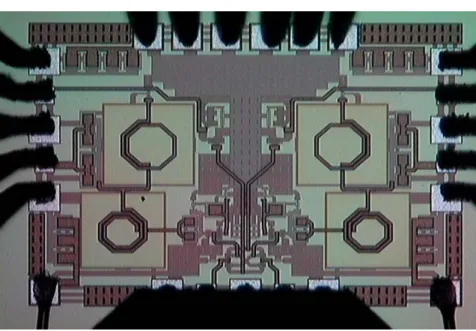
Fig. 2.5 shows the layout of the proposed UWB low power mixer. In order to decrease the degree of mismatches, the layout is as symmetrical as possible. Fig. 2.6 is the die photograph of the proposed UWB low power mixer.
Fig. 2.5 Layout of the proposed UWB low power mixer
- 9 -
The UWB low power mixer is designed for on wafer circuit measurement with PCB bias network. So the layout must follow the rule of CIC’s (Chip Implementation Center’s) probe station testing rules. Fig. 2.7 shows the UWB low power mixer for on wafer circuit measurement with PCB bias network with four probes.
Fig. 2.7 On wafer circuit measurement with PCB bias network
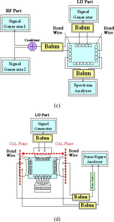
The simple measurement setups are shown in Fig. 2.8 (a-d). We use the RF IC measurement system powered by LabView to measure the linearity and conversion power gain of the UWB low power mixer. The whole measurement environment in CIC is shown in Fig. 2.9.
(a) (b)
- 10 - (c)
(d)
Fig. 2.8 Measurement setup of the proposed UWB low power mixer for (a) input return loss (b) conversion gain and P1dB (c) IIP3 (d) noise figure
- 11 -
(a)
(b)
- 12 -
I. 2.4 Measurement results and discussion
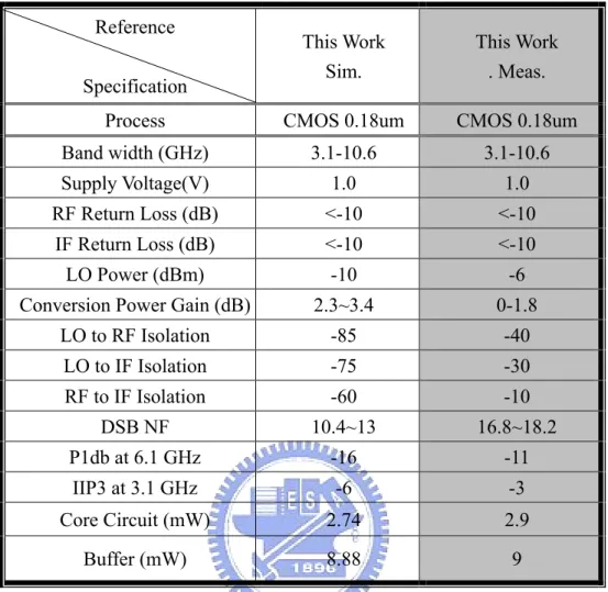
This chip size is 1.109*0.83 mm2. By the measured setups illustrated above, the measured results are listed below. The folded low power mixer consumes 2.9mA and the buffer consumes 9mA dc current with 1V supply voltage. Therefore this design dissipates only 2.9mW in core. As shown in Fig. 2.10, the measured RF port input return loss are lower than -10 dB through 3.1-10.6 GHz. As shown in Fig. 2.11, the measured IF port input return loss are lower than -10 dB through 100-528 MHz. Fig. 2.12 (a) ~ (e) shows the conversion power gain with LO power sweeping. It reveals that it only needs -6 dBm in this design to get the maximum gain. In simulation, the conversion power gain has maximum value when LO power is -10 dBm, but in measurement, the power gain has maximum value when LO power is -6 dBm. Fig. 2.13 (a) ~ (h) shows the input P1dB from 3.1 ~ 10.6 GHz with measured -11 dBm and simulated -16 ~ -18 dBm. Fig. 2.14 shows the conversion gain versus frequency from 3.1 ~ 10.6 GHz with LO power -6 dBm (measurement) and LO power -10 dBm (simulation). In measurement, the conversion gain variation in 1 dB from 3.1 ~ 9.5 GHz, and variation in 2 dB from 3.1 ~10.6 GHz. Fig. 2.15 (a) ~ (d) shows the input third order intercept point (IIP3) from 3.1 ~ 10.6 GHz with RF frequency 2 MHz separated in measurement. Because the measured setups are considered the noise of the measurement instrument, the reference level is selected lower and influenced the measured results. Fig. 2.16 shows the isolation from LO port to IF port. The LO_IF isolation is better than -30 dB from 3.1 ~ 10.6 GHz. Fig. 2.17 shows the isolation from LO port to RF port. The LO_RF isolation is better than -40 dB in UWB bandwidth. Fig. 2.18 shows the RF port to IF port isolation. The measured results are unexpected and strongly influenced by improper layout which RF port and IF port are closed.
- 13 - 0 2 4 6 8 10 12 14 16 Frequency (GHz) -30 -25 -20 -15 -10 -5 0 R F r e tu rn l o s s ( d B ) Simulation Measurement
Fig. 2.10 The measured and simulated RF return loss
0 2 4 6 8 10 12 14 16 Frequency (GHz) -26 -24 -22 -20 -18 -16 -14 -12 -10 -8 -6 -4 IF r e tu rn l o s s ( d B ) Simulation Measurement
- 14 - -25 -20 -15 -10 -5 0 5 LO Power (dBm) -12 -10 -8 -6 -4 -2 0 2 4 C o n v e rs io n G a in ( d B ) Simulation Measurement -25 -20 -15 -10 -5 0 5 LO Power (dBm) -14 -12 -10 -8 -6 -4 -2 0 2 4 C o n v e rs io n G a in ( d B ) Simulation Measurement
(a) RF frequency at 3.1 GHz (b) RF frequency at 5.1 GHz
-25 -20 -15 -10 -5 0 5 LO Power (dBm) -12 -10 -8 -6 -4 -2 0 2 4 C o n v e rs io n G a in ( d B ) Simulation Measurement -25 -20 -15 -10 -5 0 5 LO Power (dBm) -14 -12 -10 -8 -6 -4 -2 0 2 4 C o n v e rs io n G a in ( d B ) Simulation Measurement (c) RF frequency at 7.1 GHz (d) RF frequency at 9.1 GHz -25 -20 -15 -10 -5 0 5 LO Power (dBm) -14 -12 -10 -8 -6 -4 -2 0 2 4 C o n v e rs io n G a in ( d B ) Simulation Measurement (e) RF frequency at 10.6 GHz
Fig.2.12 The measured and simulated conversion gain versus LO power (a) RF frequency at 3.1 GHz (b) RF frequency at 5.1 GHz (c) RF frequency at 7.1 GHz
- 15 - -40 -35 -30 -25 -20 -15 -10 -5 0 RF Power (dBm) -25 -20 -15 -10 -5 0 5 C o n v e rs io n G a in ( d B ) Simulation Measurement -40 -35 -30 -25 -20 -15 -10 -5 0 RF Power (dBm) -20 -15 -10 -5 0 5 C o n v e rs io n G a in ( d B ) Simulation Measurement
(a) RF frequency at 3.1 GHz (b) RF frequency at 4.1 GHz
-40 -35 -30 -25 -20 -15 -10 -5 0 RF Power (dBm) -20 -15 -10 -5 0 5 C o n v e rs io n G a in ( d B ) Simulation Measurement -40 -35 -30 -25 -20 -15 -10 -5 0 RF Power (dBm) -20 -15 -10 -5 0 5 C o n v e rs io n G a in ( d B ) Simulation Measurement (c) RF frequency at 5.1 GHz (d) RF frequency at 6.1 GHz -40 -35 -30 -25 -20 -15 -10 -5 0 RF Power (dBm) -25 -20 -15 -10 -5 0 5 C o n v e rs io n G a in ( d B ) Simulation Measurement -40 -35 -30 -25 -20 -15 -10 -5 0 RF Power (dBm) -25 -20 -15 -10 -5 0 5 C o n v e rs io n G a in ( d B ) Simulation Measurement
- 16 - -40 -35 -30 -25 -20 -15 -10 -5 0 RF Power (dBm) -30 -25 -20 -15 -10 -5 0 5 C o n v e rs io n G a in ( d B ) Simulation Measurement -40 -35 -30 -25 -20 -15 -10 -5 0 RF Power (dBm) -30 -25 -20 -15 -10 -5 0 5 C o n v e rs io n G a in ( d B ) Simulation Measurement (g) RF frequency at 9.1 GHz (h) RF frequency at 10.6 GHz Fig. 2.13 The measured and simulated P1dB
(a) RF frequency at 3.1 GHz (b) RF frequency at 4.1 GHz (c) RF frequency at 5.1 GHz (d) RF frequency at 6.1 GHz (e) RF frequency at 7.1 GHz (f) RF frequency at 8.1
GHz (g) RF frequency at 9.1 GHz (h) RF frequency at 10.6 GHz 3 4 5 6 7 8 9 10 11 RF Frequency (GHz) -1 0 1 2 3 4 5 C o n v e rs io n G a in ( d B ) Simulation Measurement
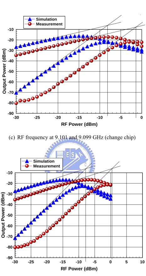
- 17 - -30 -25 -20 -15 -10 -5 0 RF Power (dBm) -80 -70 -60 -50 -40 -30 -20 -10 O u tp u t P o w e r (d B m ) Simulation Measurement
(a) RF frequency at 3.101 and 3.099 GHz
-30 -25 -20 -15 -10 -5 0 RF Power (dBm) -80 -70 -60 -50 -40 -30 -20 -10 O u tp u t P o w e r (d B m ) Simulation Measurement (b) RF frequency at 6.101 and 6.099 GHz
- 18 - -30 -25 -20 -15 -10 -5 0 RF Power (dBm) -90 -80 -70 -60 -50 -40 -30 -20 -10 O u tp u t P o w e r (d B m ) Simulation Measurement
(c) RF frequency at 9.101 and 9.099 GHz (change chip)
-30 -25 -20 -15 -10 -5 0 5 10 RF Power (dBm) -90 -80 -70 -60 -50 -40 -30 -20 -10 O u tp u t P o w e r (d B m ) Simulation Measurement
(d) RF frequency at 10.601 and 10.599 GHz (change chip)
- 19 - 3 4 5 6 7 8 9 10 11 Frequency (GHz) -50 -45 -40 -35 -30 I s o la ti o n L O _ IF Measurement
Fig. 2.16 The measured isolation LO_IF versus frequency
3 4 5 6 7 8 9 10 11 Frequency (GHz) -56 -54 -52 -50 -48 -46 -44 -42 -40 Is o la ti o n L O _ R F Measurement
- 20 - 3 4 5 6 7 8 9 10 11 Frequency (GHz) -26 -24 -22 -20 -18 -16 -14 -12 -10 -8 Is o la ti o n RF _ IF Measurement
Fig. 2.18 The measured isolation RF_IF versus frequency
3 4 5 6 7 8 9 10 11 12 13 Frequency (dB) 10 12 14 16 18 20 22 24 N o is e F ig u re ( d B ) Simulation Measurement
Fig. 2.19 The measured and simulated noise figure versus frequency
The measured results shown above reveal the good flatness from 3.1 ~ 10.6 GHz. The RF and IF port has good matching network and matches to 50 Ω. The measured conversion gain is lower than simulation 2 dB, because the post-simulation is not taking
- 21 -
all circuit into EM simulation. The measured linearity performances are better than simulation, and it is related to lower conversion gain. Linearity in mixer is dominant by the transconductance of the transconductance stage. CMOS topology as transconductance stage should be biased in moderate region to achieve maximum swing. In this design, gate bias is 0.68V in NMOS and 0.3 in PMOS. However, the linearity is bad in this bias. In mixers, transconductance dominate the linearity. Transconductance can be expressed as followed
1 2
1 2 3 ...
m m m gs m gs
g =g +g v +g v + (5),
which gm1 is the differential of the ID, gm2 is the differential of the gm1, and gm3 is the
differential of the gm2. In (5), gm1 dominates the conversion gain and gm3 dominates the
linearity. Therefore, the maximum in gm1 and minimum in gm3 can get perfect
performance. Fig. 2.20 shows gm1, gm2, and gm3 characteristic versus gate bias with
NMOS and PMOS. In Fig. 2.20 (a), the gate bias in this design (0.68V) with fixed PMOS bias at 0.3V is almost the maximum gm3 and not maximum gm1. In Fig. 2.20 (b),
the gate bias is 0.7V (1V-0.3V) with fixed NMOS bias at 0.68V, the situation is similar to Fig. 2.20 (a). Linearity and conversion gain is not the optimum value in this bias.
0 0.1 0.2 0.3 0.4 0.5 0.6 0.7 0.8 0.9 1
NMOS Gate-to-Source Voltage (V)
-0.3 -0.2 -0.1 0 0.1 0.2 0.3 0.4 gm 1 ( A /V ) gm 2 ( A /V 2) gm 3 ( A /V 3) gm3 gm2 gm1 (a)
- 22 -
0 0.1 0.2 0.3 0.4 0.5 0.6 0.7 0.8 0.9 1 PMOS Gate-to-Source Voltage (V)
-0.15 -0.1 -0.05 0 0.05 0.1 0.15 0.2 0.25 0.3 gm 1 ( A /V ) gm 2 ( A /V 2) gm 3 ( A /V 3) gm3 gm2 gm1 (b)
Fig. 2.20 Simulated gm1, gm2, and gm3 characteristic versus gate-to-source voltage
(a) NMOS (M1) (b) PMOS (M3)
The most significant influences is isolation which is worst than simulation. Because the improper layout resulted in RF to IF isolation feed-through. The RF signal can easily appear at IF port and the layout should be moderate modified. The measured noise figure is higher than simulation, and some problems happened in here. When measuring the noise figure, the measured results in conversion gain are mismatched to the other measured results which are measured in different ways. Therefore, this data should be measured again to make sure what happened. In mixer stability, this topology should be considered. Assuming the variation of Vpdc and Vndc are small, the variation
in V1 which is the drain voltage of the M1 and M3 can be expressed as following
equation [8] 1 1 1 2 mp ndc mn pdc ms op on g V g V V g R R ∆ + ∆ ∆ = − + + (6). ∆V1 is the variation drain voltage of M1 and M2, Rop and Ron are the output impedance
- 23 -
The gms dominates the equation if its value is large enough. And CMOS topology is no
need for common mode feedback. However, in practice measurement, the mixer is sensitive in variation of Vpdc and Vndc. Because CMOS transconductance stage input
versus output characteristic is as following if Vdd is 1V without capacitor.
0 0.2 0.4 0.6 0.8 1 Vi (V) 0 0.1 0.2 0.3 0.4 0.5 0.6 0.7 0.8 0.9 1 V o ( V ) Vi_Vo Curve
Fig. 2.21 CMOS input voltage versus output voltage
The moderate operation is only at 0.48V for two transistors. In the abnormal operating region in CMOS, the performance will be limited. In this design, Fig. 2.22 is shown with fixed Vpdc at 0.3V. In measured biasing voltage, the 10% variation of Vndc let
CMOS operating out of saturation region. The moderate bias is important in mixer design.
0 0.2 0.4 0.6 0.8 1
Gate bias of NMOS (V)
0 0.1 0.2 0.3 0.4 0.5 0.6 0.7 0.8 0.9 1 V 1 ( V ) Vi_Vo_PMOS_0.3V
Fig. 2.22 CMOS input voltage versus output voltage with capacitor C
- 24 -
Table 2.1 Simulated and measured performance of the folded low power mixer Reference Specification This Work Sim. This Work . Meas.
Process CMOS 0.18um CMOS 0.18um
Band width (GHz) 3.1-10.6 3.1-10.6
Supply Voltage(V) 1.0 1.0
RF Return Loss (dB) <-10 <-10
IF Return Loss (dB) <-10 <-10
LO Power (dBm) -10 -6
Conversion Power Gain (dB) 2.3~3.4 0-1.8
LO to RF Isolation -85 -40 LO to IF Isolation -75 -30 RF to IF Isolation -60 -10 DSB NF 10.4~13 16.8~18.2 P1db at 6.1 GHz -16 -11 IIP3 at 3.1 GHz -6 -3 Core Circuit (mW) 2.74 2.9 Buffer (mW) 8.88 9
- 25 -
Section II
Low Power Mixer with Flicker Noise Improved
Technique
II. 2.1 Introduction
Rapid development of wireless communication, the target is low power and low cost system. For receivers of communication system, direct conversion receiver (DCR) is most popular type. In the direct conversion system, flicker noise is strong influenced on noise figure and sensitivity. Some problems are presented for DCR with CMOS technology. The critical problem is the noise influence [1]. And there are important repercussions in DCRs [2]. The flicker noise (1/f) of the mixer degrades SNR (signal-to-noise ratio) at the output baseband.
Because of good isolation, Gilbert cell is the most popular topology for using. Gilbert cell has good isolation for LO-IF and LO-RF and symmetric balance [3]. For application in Gilbert cell mixer of DCR, the noise is influence in flicker noise. The flicker noise in active mixer is discussed as followed.
II. 2.2 Flicker Noise in Mixers
CMOS transistors suffer from high flicker noise which is inversely proportional to the device area [4]. This is produced from CMOS process and unable avoided. So the size of CMOS transistor is influenced in flicker noise.
Double balanced mixer in DCRs comprises transconductance stage, switch stage with local oscillator, and IF loaded stage. Because flicker noise in RF stage is low frequency noise, it will be up-converted to vicinity of LO frequency. And it will not contribute any flicker noise in DCR systems. Load stage is used of polysilicon resistors which are free of flicker noise. Mismatches in the switch pairs will also
- 26 -
generate a small amount of flicker noise at the output. Therefore, switch stage is significant contributed flicker noise at baseband [5].
Flicker noise in DCRs is determined in switch pair devices. There are two different mechanisms that generate flicker noise. The first one is direct mechanism, which is generated in the switching transitions. When LO stage commutating motion, it will generate noise pulse trains. Because noise transfer function is linear from each device, the superposition theory holds. The low frequency in switching pairs should be calculated as the voltage source Vn(t). Fig. 2.23 shows the noise pulses resulting in
flicker noise at mixer output [6]. Because mixer needs sine wave of local oscillator to drive switching quad, the large sine-wave LO signal accompanies noise. The noise advances or retards the time of zero crossing by ∆t=Vn(t)/S. So the noise pulse trains
of random widths ∆t and amplitude of 2I at a frequency of 2ωLO represent at the
output.
Fig. 2.23 Noise pulses resulting in flicker noise at mixer output [6]
( )
n V t t S ∆ = (7)Over one period, the average of output current is [5]
, 2 2 4 2 2 n o n n V I i I t I V T T S ST = × × ∆ = × × = (8)
- 27 - 2 f n eff eff ox K V W L C f = × (9),
where I is the bias current of RF transconductance stage, T is the LO period, Vn is the
flicker noise of switch pairs, and S is the slope of the LO signal. Weff and Leff are the
effective width and length, Cox is the oxide capacitance, f is frequency, and Kf is a
process parameter [5]. In the indirect mechanism, capacitance Cp is main determined
flicker noise. It can describe as following equation
(
)
(
)
2 , 2 2 2 p p LO o n n ms p LO C C i V T g C ω ω = × + (10),where Cp is the tail capacitance between LO switch stage and RF transconductance
stage with all parasitic capacitance. T is the LO period, gms is the transconductance of
LO switches, ωLO is the frequency of local oscillator, and Vn is equivalent flicker
noise of LO switches [5].
So, there are some topologies to reduce flicker noise from above equation. From (8), increasing the slope of the LO signal and reducing the equivalent flicker noise of switching transistors can alleviate the influence. It needs to increase sizes of the switch transistors. However, it has some drawbacks. The large sizes of switching transistors increase the parasitic capacitance at common source of switch stage and increase the flicker noise indirectly.
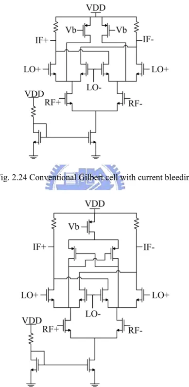
Reduction of bias current of the switch stage can lower the noise pulses and improve flicker noise. Conventional Gilbert cell with current bleeding is proposed in Fig. 2.24. However, this technique has some important drawbacks. When reducing the biasing current of the switch pairs, the impendence as seen from RF transconductance stage into switch stage (1/gms) will be increased. It allows more RF
leakage current flowing into the bleeding circuit. The leakage current will also be shunt by the parasitic capacitance at the node between RF stage and switch stage.
- 28 -
This decreases the gain and reduces the mixer linearity. The dynamic current bleeding circuit is proposed to solve the problems [6]. Fig. 2.25 is presented the conventional Gilbert cell mixer with dynamic current bleeding.
Fig. 2.24 Conventional Gilbert cell with current bleeding
- 29 -
Since the noise pulse trains is only present at the switching instant of LO switch quads. A dynamic current bleeding is injected to the core through a switch control circuit at the switching instant of switch pairs. Fig. 2.26 shows the theory and idea for dynamic current bleeding [6]. The switching event controls by the nodes at common source of switch pairs (Fig. 2.26 nodes A and B). The waveform of nodes A and B is shown in Fig. 2.26 (b). Because the LO provides large signal, the voltage waveforms at nodes A and B are just like full wave rectifiers. The injection of dynamic current ID
occurs when voltage is small. This way reduces the height of noise pulse directly, and noise pulse at the output is close to zero as shown in Fig. 2.26 (b). On the other time, the switch is close and generates no current to circuit.
Fig. 2.26 (a) Dynamic current injection (b) Nodes waveform [6]
There are a few drawbacks in this topology. It needs high power of LO to drive switch stage and its conversion gain is low. It is just like a passive mixer. In spite of the imperfect of switching, this technique is still improved significant.
- 30 -
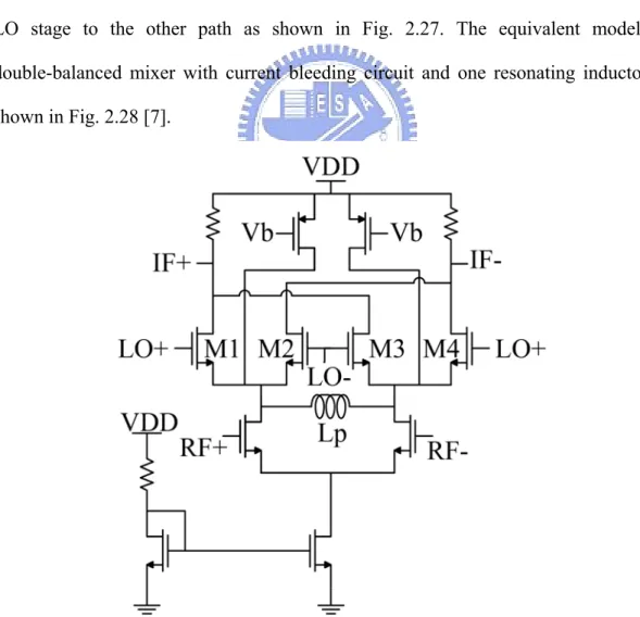
stage and tuning out the tail capacitance from (8) and (10). Current bleeding technique is decreased the bias current of the switch stage, and has a few drawbacks described above. Fig. 2.27 shows the conventional Gilbert cell mixer with current bleeding and one resonating inductor. Even though the current bleeding can reduce to LO bias current to improve flicker noise, it is generated the flicker noise from tail capacitance in indirectly mechanism. In order to diminish the tail capacitance, the choice of small size device in RF and LO stage is an idea. Nevertheless, CMOS transistors suffer from high flicker noise which is inversely proportional to the device area [4]. So the other way is using one inductor to tune out the tail capacitance instead of changing the size of MOS. The inductor is connected from one path at the nodes between RF and LO stage to the other path as shown in Fig. 2.27. The equivalent model of double-balanced mixer with current bleeding circuit and one resonating inductor is shown in Fig. 2.28 [7].
- 31 -
Fig. 2.28 Equivalent model of double-balanced mixer with current bleeding circuit and one resonating inductor [7]
The gm1 is the transconductance of the switch transistor M1, and gm2, gm3, gm4 are the
same as gm1. Cp is the parasitic capacitance at the node of transconductance stage and
switch stage. RB is the load of the transistor as current bleeding. Lp is the resonating
inductor. As shown in Fig. 2.28, the resonating inductor tunes out the tail capacitance and protects RF signal current from flowing into shunt path. This technique improves conversion gain and flicker noise simultaneously. So this technique is adopted in our design. The significant improvement is presented.
- 32 -
II. 2.3 Low Power Mixer with Flicker Noise Improved
Technique
Fig. 2.29 the proposed low power mixer with low flicker noise
Fig. 2.29 shows the proposed mixer with improved flicker noise. Low power mixer is described in Section I. Improving flicker noise, understanding the physic mechanism in active mixer is first important. From equation (8) and (10), reducing the bias current of LO switch stage and reducing the influence from tail capacitance is the direction. In this request, we use one resonating inductor technique in low power mixer, which is proposed in Section I. As shown in Fig. 2.29, the current reusing in
- 33 -
RF transconductance stage can reduce the LO bias current and enhance the transconductance of RF stage simultaneously. We would not repeat this part of low power mixer here. In this topology, the low DC current in LO switch stage by current reused in RF stage is achievable. First, lowering the bias current of LO stage is natural by this topology. However, the tail capacitance effect is still existence and generated flicker noise indirectly. Therefore second, tuning out the parasitic capacitance is the best way to improve flicker noise. The parasitic capacitances at the nodes between LO switch stage and RF transconductance stage can be tuned out by resonant inductor at 2fo. We choose small size of LO switch transistors to switch quickly, though the LO
switching device suffers from intrinsic flicker noise which inversely to proportional device area. The load is used polysilicon resistor which is free of flicker noise. RF transconductance stage is contributed no flicker noise at output as described before. The improvement of flicker noise in active low power mixer is significant. This design achieves low power, low cost, moderate gain, linearity, and improving flicker noise in DCR systems. Fig. 2.30 and Fig. 2.31 show the improvement with and without the inductor. Fig. 2.30 is presented the conversion gain is improved by 4 dB. Fig. 2.31 is shown the flicker noise is reduced and noise figure is decreased 3 dB at 10 MHz.
- 34 - -25 -20 -15 -10 -5 0 5 LO Power (dBm) -8 -6 -4 -2 0 2 4 6 8 C o n v e rs io n G a in ( d B ) With inductor L Without inductor L
Fig. 2.30 The simulated conversion gain with and without resonant inductor L
1000 10000 100000 1E+006 1E+007 Frequency (Hz) 10 15 20 25 30 35 40 45 N o is e F ig u re ( d B ) With inductor L Without inductor L
Fig. 2.31 The simulated noise figure with and without resonant inductor L
The important index in flicker noise improvement is the flicker noise corner frequency. The 1/f flicker noise corner frequency is defined as the frequency where the flicker noise and thermal noise components intersect. The corner is reduced as shown in Fig. 2.31.
- 35 -
II. 2.4 Chip implementation and measured consideration
Fig. 2.32 shows the layout of the proposed low power mixer with flicker noise improved technique. In order to decrease the degree of mismatches, the layout is as symmetrical as possible. Fig. 2.33 is the die photograph of the proposed low power mixer with improving flicker noise.
- 36 -
Fig. 2.33 Die photograph of the proposed UWB low power mixer
The low power mixer is designed for on wafer circuit measurement. So the layout must follow the rule of CIC’s (Chip Implementation Center’s) probe station testing rules. Fig. 2.34 shows the low power mixer for on wafer circuit measurement with four probes.
Fig. 2.34 On wafer circuit measurement
The simple measurement setups are shown in Fig. 2.35 (a-d). We use the RF IC measurement system powered by LabView to measure the linearity and conversion
- 37 -
power gain of the low power mixer with improving flicker noise.
(a) (b)
(c)
(d)
Fig. 2.35 Measurement setup of the proposed folded mixer with improving flicker noise for (a) input return loss (b) conversion gain and P1dB (c) IIP3 (d) noise figure
- 38 -
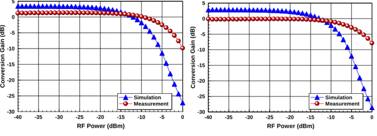
II. 2.5 Measurement results and discussion
This chip size is 1.042*1.102 mm2. In this section, the simulated and measured results are shown below. The low flicker noise and low power mixer consumes 3.8mA and buffer consumes 8.8 mA dc current with 1V supply voltage. Therefore this design dissipates only 3.8 mW in core. This design operating frequency is at 5.2 GHz. Fig. 2.36 shows RF port return loss. RF return loss is below -15 dB at 5.2 GHz. Fig. 2.37 shows LO power versus conversion gain. When LO power is -10 dBm in simulation and -6 dBm in measurement, the conversion gain can obtain the maximum gain. Fig. 2.38 shows P1dB at 5.2 GHz and Fig. 2.39 shows the input third order intercept point (IIP3) with RF frequency 2 MHz separated in measurement. The P1dB is -16 dBm in measurement and -18 in simulation. The IIP3 is -6 dBm in measurement and -8 in simulation. The two illustrations reveal linearity of this mixer. The double sideband (DSB) noise figure is close to 10 dB at 100 MHz in simulation, and in practice, the DSB noise figure is close to 13 dB at 100 MHz. The DSB NF at 10 MHz is 17 dB in measurement and 11.4 dB in simulation as shown in Fig. 2.40. Isolation including LO-to-IF, LO-to-RF, and RF-to-IF are also measured. In LO power is -6 dBm, LO-to-IF isolation is -57 dB, LO-to-RF isolation is -61 dB, and RF-to-IF isolation is -39 dB.
- 39 - 0 2 4 6 8 10 12 Frequency (GHz) -30 -25 -20 -15 -10 -5 0 R F R e tu rn L o s s ( d B ) Simulation Measurement
Fig. 2.36 The simulated and measured RF return loss
-15 -10 -5 0 5 LO Power (dBm) -2 0 2 4 6 8 10 C o n v e rs io n G a in ( d B ) Measurement Simulation
- 40 - -40 -35 -30 -25 -20 -15 -10 -5 0 RF Power (dBm) -25 -20 -15 -10 -5 0 5 10 C o n v e rs io n G a in ( d B ) Measurement Simulation
Fig. 2.38 The simulated and measured P1dB
-40 -35 -30 -25 -20 -15 -10 -5 0 RF Power (dBm) -100 -90 -80 -70 -60 -50 -40 -30 -20 -10 0 O u tp u t P o w e r (d B m ) Measurement Simulation
- 41 - 0 2 4 6 8 10 12 IF Frequency (10 MHz) 10 11 12 13 14 15 16 17 18 D S B N o is e F ig u re ( d B ) Measurement Simulation
Fig. 2.40 The simulated and measured noise figure versus IF Frequency
Because of the moderate layout, the isolation is improved by a wide margin, especially in RF-to-IF. The technique variation is influence in this design. The measured dc in mixer core is higher than simulation, and the measured dc in buffer is lower than simulation. The incomplete EM post-simulation is the reason why the conversion gain is lower than simulation. The target improving flicker noise is achieved in this design. The simulated and measured results are in Table 2.2. Because the flicker noise is not lower enough to mixer, the improvement is presented in Chapter 4 future work in this thesis.
- 42 -
Table 2.2 Simulated and measured performance of the folded low power mixer with improving flicker noise
Reference Specification This Work Sim. This Work . Meas.
Process CMOS 0.18um CMOS 0.18um
Operating Frequency (GHz) 5.2 5.2
Supply Voltage(V) 1.0 1.0
RF Return Loss (dB) <-10 <-10
IF Return Loss (dB) <-10 <-10
LO Power (dBm) -10 -6
Conversion Power Gain (dB) 7.8 5.8
LO to RF Isolation -41 -61 LO to IF Isolation -70 -57 RF to IF Isolation -75 -39 DSB NF(at 10 MHz) 11.4 17 P1dB -18 -16 IIP3 -8 -6 Core Circuit (mW) 3.46 3.8 Buffer (mW) 9.18 8.8
- 43 -
II. 2.6 Comparison
Section I and Section II are proposed two mixers. Section II utilizes Section I low voltage mixer to improve its flicker noise. From the measured results, the conversion gain enhances 4.5 dB and noise figure reduces 4 dB. The goal is implemented in this design. Table 2.3 shows this two mixer performance at 5.2 GHz.
Table 2.3 Measured results with and without inductor Reference
Specification
Low Power Mixer Low Power Mixer with Inductor
Process CMOS 0.18um CMOS 0.18um
Operating Frequency (GHz) 5.2 5.2
Supply Voltage(V) 1.0 1.0
RF Return Loss (dB) <-10 <-10
IF Return Loss (dB) <-10 <-10
LO Power (dBm) -6 -6
Conversion Power Gain (dB) 1.2 5.8
LO to RF Isolation -45 -61 LO to IF Isolation -42 -57 RF to IF Isolation -12 -39 DSB NF(at 100 MHz) 17 13 P1dB -10 -16 IIP3 -3 -6 Core Circuit (mW) 2.9 3.8 Buffer (mW) 9 8.8
- 44 -
Chapter 3
Ultra Low power mixer
3.1 Introduction
As the progressing of the times, the MOS scaling is reduction speedy. With the down scaling of the transistors, it is severe with supply voltage. In the RF receiver, low cost and low consumption is first consideration. The demands for low power wireless transceivers operating GHz band are more critical. In order to achieve low power consumption, circuit topologies combine LNA with mixer for current reuse [1] or combine oscillator with mixer [2]. Transformer-based mixer [3] is presented for low power consumption. By subthreshold biasing of MOS transistor, subthreshold mixer is proposed for Ultra low power [4].
Fig. 3.1 shows a single balance mixer. It is often used in RF receivers and frontends. The transistor M1 as a transconductance converts RF signal into current and commutates at M2 and M3 for frequency translating. The signal current converts to voltage through load resistor at IF. With this topology, it is not suitable for low supply voltage and power application. Folded mixer is presented for solving the problem [5]. Although folded mixer can reduce the supply voltage, it does not reuse DC current and may increase power consumption. Fig. 3.2 shows a complementary current reused mixer [6]. This topology comprises DC current reused and low supply voltage at the same time. In order to enhance conversion gain, current bleeding technology is adopted [7]. Fig. 3.3 is presented complementary current reused mixer with current bleeding technique.
- 45 -
Fig. 3.1 Single balance mixer
Fig. 3.2 Complementary current reused mixer
- 46 -
3.2 Ultra low power mixer
Fig. 3.4 The proposed Ultra low power mixer
Fig. 3.4 shows the proposed circuit. The complementary current reused topology technique is adopted for this single balance mixer. The RF voltage signal converts to current through transistor M1 and M2 (transconductance stage), and then the current coupled to the sources of M3 and M4 (switch stage) through capacitor C2. The resistors R2 and R3 are used to load resistors. The load resistors are as large as possible to achieve high conversion gain. After translating frequency to IF band, the common drain output buffer is connected to switch stage and load resistors. In DC analysis, the complementary current reused topology provides low power consumption and low supply voltage. Transconductance stage utilizes PMOS stacked on the top of the NMOS just like an inverter. The inverter can not only provide current bleeding technique and enhance the transconductor of the transconductance stage. Therefore in the AC analysis,
- 47 -
the RF signal is converted through M1 and coupled to M2 and then commutating at M3 and M4 through capacitor C2. RF input network employs source degeneration with inductors L1 and L2 to reach input matching network and signal amplification.
Transconductance of the switch stage transistors M3 and M4 is influenced with conversion gain [6]. If gm3 is large enough, the conversion gain is independent of switch
stage. On the contrary, gm3 is not sufficient and conversion gain will be decreased. The
bleeding current affects transconductance of the switch stage and gain. The choice of the ratio is important for current bleeding technology. Fig. 3.5 shows conversion gain versus ratio of current bleeding. The gain can be achieved maximum at the vicinity of 60 to 70 percent of the ratio. Fig. 3.6 shows noise figure versus ratio of current bleeding. Noise figure can be achieved minimum at the vicinity of 65 to 70 percent. Hence, the moderate selection of the ratio of current bleeding can achieve ideal performance in conversion gain and noise figure.
0.5 0.55 0.6 0.65 0.7 0.75 0.8 Ratio of current bleeding (%)
0 0.5 1 1.5 2 2.5 C in v e rs io n g a in ( d B )
- 48 -
0.55 0.6 0.65 0.7 0.75 0.8 Ratio of current bleeding (%)
12.15 12.2 12.25 12.3 12.35 12.4 12.45 12.5 12.55 12.6 N o is e f ig u re ( d B )
Fig. 3.6 Noise figure versus Ratio of current bleeding
Linearity in the RF receivers and front ends is influenced by the mixer. Linearity dominated with transconductance of the mixer for ideal switches. In the transconductance stage, the nonlinearity elements are generated from gm
(transconductance), gds (output conductance), and Cgs (gate-source capacitance).
Linearity of overall mixer is dominant from gm [8], [9]. Transconductance g can be m
expressed by Taylor series as follows
1 2
1 2 3 ...
m m m gs m gs
g =g +g v +g v + . (11)
And the drain current can be expressed by Taylor series as follows
( )
( )
2( )
3( )
1 2 3 ...
d m gs m gs m gs
i t =g v t +g v t +g v t + (12)
The harmonic elements should be decreased or canceled out. In addition to nonlinearity elements, the gate bias of transistors M1 and M2 are strongly influenced for linearity. The choice of appropriate gate bias can reduce harmonic effects [6], especially the “sweet spot” [10]. The moderate bias at the vicinity of sweet spot enhances the linearity. Therefore, the trade-off between conversion gain, noise figure, and linearity should be considered.
- 49 -
3.3 Chip implementation and measured consideration
Fig. 3.7 shows layout of the proposed mixer. The proposed circuit is designed for on-wafer measurement. It follows the rules of CIC’s (Chip Implementation Center’s) probe station testing rules.
Fig. 3.7 Layout of the proposed mixer
The Ultra low power mixer is designed for on wafer circuit measurement. So the layout must follow the rule of CIC’s (Chip Implementation Center’s) probe station testing rules. Fig. 3.8 shows the Ultra low power mixer for on wafer circuit measurement with four probes.
- 50 -
The simple measurement setups are shown in Fig. 3.9 (a-d). We use the RF IC measurement system powered by LabView to measure the linearity and conversion power gain of the Ultra low power mixer.
(a) (b)
- 51 - (d)
Fig. 3.9 Measurement setup of the proposed UWB low power mixer for (a) input return loss (b) conversion gain and P1dB (c) IIP3 (d) noise figure
3.4 Simulation result and discussion
In this section, the simulated results are shown below. We set operating frequency at 5.2 GHz. Fig. 3.10 shows RF return loss. RF return loss is below -20 dB at 5.2 GHz. Fig. 3.11 shows LO power versus conversion gain. When LO power is -9 dBm, the conversion gain can obtain the maximum gain. Fig. 3.12 shows P1dB and Fig. 3.13 shows the input third order intercept point (IIP3). The two illustrations reveal linearity of this mixer. This mixer has simulation P1dB of -19 dBm, and IIP3 of -8 dBm. The double sideband noise figure is close to 11.25 dB at 5.2 GHz as shown in Fig. 3.14.
- 52 - 0 2 4 6 8 10 12 14 RF Frequency (GHz) -25 -20 -15 -10 -5 0 R F R e tu rn L o s s ( d B ) Simulation
Fig. 3.10 The simulated RF return loss
-16 -14 -12 -10 -8 -6 -4 -2 LO Power (dBm) -3 -2.5 -2 -1.5 -1 -0.5 0 0.5 1 1.5 2 C o n v e rs io n G a in ( d B ) Simulation
![Fig. 2.23 Noise pulses resulting in flicker noise at mixer output [6]](https://thumb-ap.123doks.com/thumbv2/9libinfo/8471460.183556/38.892.135.765.487.1088/fig-noise-pulses-resulting-flicker-noise-mixer-output.webp)