Impact of the strained SiGe source/drain on hot carrier reliability for 45 nm
p-type metal-oxide-semiconductor field-effect transistors
C. Y. Cheng,1Y. K. Fang,1,a兲J. C. Hsieh,2H. Hsia,2W. M. Chen,2S. S. Lin,2and C. S. Hou21
VLSI Technology Laboratory, Institute of Microelectronics, Department of Electrical Engineering and Advanced Optoelectronic Technology Center, National Cheng Kung University, Tainan, Taiwan 701, Taiwan, Republic of China
2
Taiwan Semiconductor Manufacturing Company, 8 Li-Hsin Rd 6, Hsinchu Science Park, Hsinchu, Taiwan 300, Taiwan, Republic of China
共Received 13 December 2007; accepted 11 March 2008; published online 1 April 2008兲
In this letter, the impact of the uniaxial strain SiGe source/drain共S/D兲 on hot carrier reliability in 45 nm p-type metal-oxide-semiconductor field-effect transistor is investigated in detail. We find that the extra mechanical stress deteriorates the gate oxide and/or generates interface states significantly, resulting in the hot carrier degradation dominantly driven by the drain avalanche hot carrier stress 共Vg= 1/2Vd兲, as opposed to the channel hot electron stress 共Vg= Vd兲, the well-known dominant mechanism for hot carrier degradation in the conventional deep submicron devices. A model to explain the mechanism of these observations is proposed. © 2008 American Institute of Physics. 关DOI:10.1063/1.2904647兴
As the gate-oxide thickness in the complementary metal-oxide-semiconductor共CMOS兲 technology continues to scale down, it becomes inevitably more vulnerable under a high electric field. Consequently, the gate oxide and oxide-silicon interface are deteriorated significantly after hot carrier stress 共HCS兲. For conventional deep submicron devices, the domi-nant mechanism of device degradation under HCS changes from the drain avalanche hot carriers 共DAHC兲 injection at the maximum substrate current Isub共Vg= 1/2Vd兲 共Ref. 1兲 to the channel hot electron injection共CHE兲 under the maximum gate voltage共Vg= Vd兲.
2–5
On the other hand, the strain engi-neering such as the embedded SiGe source/drain 共S/D兲 has been extensively utilized to improve p-type MOS field-effect transistor共p-MOSFET兲 carrier mobility6–8and implemented widely in today’s state-of-the-art p-MOSFET fabrication. For the deep nanodevices, it is highly suspected that the extra mechanical stress from strain engineering would further de-teriorate gate oxide and/or interface and the strain effect would intensify the HCS degradations. However, so far, no clear studies about the influence of the mechanical stress on HCS reliability characterization have been reported. In the past, for p-MOSFETs, most of studies have been focused on the negative bias temperature instability,9,10 and been ne-glected for the HCS reliability because the mean free path of holes in silicon is shorter than that of the electrons and holes scatter more frequently and fewer holes could gain enough energy 共about 4 eV兲 to deteriorate the interface and/or gate dielectric. Nevertheless, as p-MOSFET device is scaled down to deep nanoregime, both HCS reliability and the in-fluence of a mechanical stress could not be ignored for its very small dimension.
In this letter, we report the impact of the uniaxial strain SiGe S/D on the HCS reliability in 45 nm p-MOSFETs. Ex-perimental results show that the extra mechanical stress from the SiGe S/D would cause more serious degradations after the DAHC type stress than that after CHE type stress, a fact
that is contrary to the conventional deep submicron device without strained SiGe S/D.
The p-MOSFET devices with width/length ratio of 10/0.1 were fabricated by a state-of-the-art 45 nm CMOS foundry technology on共100兲 silicon substrates.11After shal-low trench isolation and gate formation, the in situ boron doped p+ Si
0.8Ge0.2 S/D with boron concentration of 1018– 1019cm−3 is selectively deposited under ultravacuum at 600 ° C. The gate is boron doped p+ polysilicon with a 1.6– 1.7 nm nitride oxide grown by a decoupled plasma ni-tridation. In order to protect the gate damages from the SiGe S/D recess etching, before etching, we deposit a tetraethy-lorthosilicate film and a nitride film as the hard mask共HM兲. Then the HM is removed after SiGe deposition. The trans-mission electron microscopy examination shows intact S/D junction and no damages induced by the S/D recess etching. Subsequently, processes of lightly-doped drain implant, spacer formation, postimplantation rapid thermal annealing 共RTA兲 共at 900 °C for 30 s兲, and back-end process were implemented to complete the devices. With the RTA, the damages induced by the recessing S/D etching can be re-duced to a minimum. For comparison purposes, devices without SiGe S/D are also fabricated under the same process-ing conditions.
The HCS degradations were investigated by the widely used charge pumping 共CP兲 method.12–15 Both DAHC and CHE stress modes are investigated. The devices were stressed under Vg= Vd= −2 V and Vg= 1/2Vd= −1 V for the CHE and the DAHC modes, respectively. In both stress modes, the source/substrate was grounded and the drain was connected to Vd. The stress time was set to 500 and 5000 s. The CP measurements were performed using a pulse genera-tor共Agilent-8110兲 and a precision semiconductor parameter analyzer共Agilent-4156C兲 under the conditions of 1.5 V gate pulse, 1 MHz frequency, −0.1 V reversely biased S/D, and 80 ns of pulse rise /fall time, respectively.
Figure 1 illustrates the schematic cross section of our 45 nm p-MOSFET device with strained SiGe S/D. In gen-eral, there are some sources to deteriorate the ultrathin gate
a兲Electronic mail: [email protected].
APPLIED PHYSICS LETTERS 92, 133504共2008兲
0003-6951/2008/92共13兲/133504/3/$23.00 92, 133504-1 © 2008 American Institute of Physics
dielectric and interface for the interface states 共Nit兲 genera-tion. One is the compressively mechanical stress resulted from the lattice mismatch between Si and SiGe 共aSi = 5.430 95 Å, aSiGe= 5.4806 Å兲. The mechanical stress in the channel decreases with the distance from the SiGe drain and has a maximum value located at the drain side, as shown in Fig.2, theT-CAD共Technology Computer Aided Design
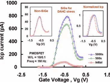
pack-age兲 simulated stress distribution in our p-MOSFET device. The maximum mechanical stress will cause the maximum damages of the channel located at the drain side关i.e., region III in Figs.1 and 2共b兲兴. Another source is the high electric field resulted from the HCS. Under the CHE mode stress, the largest field occurs between the gate and the channel 共Vg− Vsub= −2 V兲. As a result, most of damages take place at regions I and II, as illustrated in Fig.1. For the DAHC mode stress, the field in the channel is lower共Vg− Vsub= −1 V兲 and hence the hot carries should be accelerated continuously un-til arriving the drain side to gain enough energy for ava-lanche impact ionization. The impact ionization creates a substrate current and injection of hot carrier into the gate dielectric共Vg− Vd= 1 V兲, resulting in the maximum damages presented at the drain side 共region III兲. These damages can be evaluated by the measurements of CP current共ICP兲. Figure
3gives the measured ICPunder DAHC stress mode for vari-ous stress time in both SiGe and non-SiGe devices, respec-tively. In the non-SiGe devices, the ICP current with 500 or 5000 s stress is almost identical. This means that when the channel is scaled, only the DAHC electric field stress alone does not induce serious HCS degradation. However, in the SiGe S/D devices, the initial ICPis 76.6 pA, larger than the 51 pA in the non-SiGe devices, implying that the gate and interface indeed have been damaged by the SiGe S/D me-chanical stress. In addition, with increasing stress time, the ICP current of SiGe device significantly increases as com-pared to the slight increase of ICP current in the non-SiGe S/D counterpart. Our data clearly manifest that the strained SiGe S/D enhances the DAHC stress mode HCS degrada-tion. In addition, the inset on the right of Fig.3 shows that the normalized ICP bell-like curves after 500 and 5000 s stress are shifted toward the positive Vgvoltage. The positive
Vg shift can be attributed to the hot electrons trapped in the gate dielectric. In the contrary, as shown in Fig. 4, in the CHE stress mode, the ICPcurrents for various stress time are less than that under DAHC stress mode, although the initial ICP current of the SiGe devices is larger than that of non-SiGe counterparts. This is reasonable because most of the damages caused by the strained SiGe S/D are located near FIG. 1. 共Color online兲 The schematic cross section of a p-MOSFET with
strained SiGe S/D illustrates the different mechanisms between DAHC and CHE stress modes and the defects generated by the SiGe S/D compressive stress. The defects are marked by “XX,” where I is lightly damaged region, II is averagely damaged region, and III is heavily damaged region. The bottom left inset lists the table for comparison of the Vtshift, Idsat degrada-tion and generated Nitafter various stress modes with a stress time of
5000 s. The⫹ and ⫺ means an increasing or decreasing for the amount after the stress from the initial one. The top left inset illustrates the mecha-nism of the enhanced ICPin the higher Vgregion after the CHE stress.
FIG. 2. 共Color online兲 T-CAD simulated compressive stress contour of a
45 nm p-MOSFET with strained SiGe S/D共a兲 the cross section and 共b兲 lateral distribution in channel.
FIG. 3. 共Color online兲 The charge pumping current 共ICP兲 of p-MOSFETs
with and without strained SiGe S/D as a function of gate voltage共Vg兲 with different stress times under the DAHC stress mode. The inset on the right compares the normalized ICPof the p-MOSFETs with strained SiGe S/D
after various DAHC stress time. The shift in positive Vgafter the DAHC stress is proportional to the stress time.
133504-2 Cheng et al. Appl. Phys. Lett. 92, 133504共2008兲
drain side. Moreover, even the field direction in the strained SiGe S/D is preferable for hot holes injection, the barrier height of SiO2/Si for holes is too high 共larger than 4 eV兲 to inject carriers and, hence, no ICP-Vgcurve shift is found共the inset on the right of Fig. 4兲. Furthermore, the ICP current increases in the positive Vg region with the stress time, clearly indicating that the ICPin region II is enhanced by the SiGe mechanical stress, as illustrated in the inset of top left Fig.1. In other words, the behaviors of hot carriers are dif-ferent for two HCS modes in the presence of strained SiGe S/D. Furthermore, other source such as the recessing S/D etching-induced damages may contribute to the hot carrier degradations. Conventionally, this etching-induced damage will induce S/D leakage; however, in this work, due to the addition of hard mask and RTA, the damages are dramati-cally reduced. Thus, its effect on hot carrier degradation be-comes minor, as compared to the SiGe mechanical stress and high electric field resulted from the HCS.
We also compare the threshold voltage shifts共⌬Vt兲, satu-ration current degradations共⌬Idsat兲, and number of interface states共Nit兲 in both SiGe and non-SiGe devices after 5000 s for DAHC and CHE stress modes, respectively.共Please see the table inserted in Fig.1, where the “⫹” and “⫺” means
the “increasing” and “decreasing” for the amount after the stress from the initial value, respectively.兲 In the non-SiGe devices, the increasing of Nit number after CHE mode stress 共44.54%兲 is larger than that after DAHC stress 共5.53%兲, sug-gesting that the CHE mode dominates the HCS degradation, a well-known phenomena in the deep submicron devices.2,3 However, in the SiGe devices, Nit after DAHC stress mode increases substantially to 945.12%, much larger than 57.8% after CHE stress mode. Similar observation is found on the ⌬Vt and Idsat degradations as well. Clearly, the dominant
mechanism of HCS degradation is the DAHC stress mode in the presence of strained SiGe S/D.
In summary, the HCS degradations in 45 nm p-MOSFETs with and without uniaxial strain SiGe S/D have been investigated and compared. The strained SiGe S/D sig-nificantly enhances the hot carrier damages at the interface and gate oxide, especially near to the drain. Consequently, the dominant mechanism of HCS degradation in the strained SiGe S/D devices is found to be different from that in non-strained devices. Thus, it is suggested the influence of me-chanical stress on HCS degradation could be more severe in the advanced deep nano devices for the further dimension scaling.
This work was supported by the National Science Coun-cil under Contract No. NSC96-2221-E-006-284-MY3, and by TSMC, under Contract No. E041510. The authors would also like to thank TSMC for their continuous support and Dr. K. C. Ku for his critical reading of the manuscript.
1E. Takeda, A. Shimizu, and T. Hagiwara, IEEE Electron Device Lett. EDL-4, 329共1983兲.
2S.-G. Lee, J.-M. Hwang, and H.-D. Lee,IEEE Trans. Electron Devices 49, 1876共2002兲.
3L. Su, S. Subbanna, E. Crabbe, P. Agnello, E. Nowak, R. Schulz, S.
Rauch, H. Ng, T. Newman, A. Ray, M. Hargrove, A. Acovic, J. Snare, S. Crowder, B. Chen, J. Sun, and B. Davari, Tech Dig. VLSI Symp 1996, 12.
4K. Takeuchi, T. Yamamoto, A. Tanabe, T. Matsuki, T. Kunio, M. Fukuma,
K. Nakajima, H. Aizaki, H. Miyamoto, and E. Ikawa, Tech. Dig. - Int. Electron Devices Meet. 1993, 883.
5E. Li, E. Rosenbaum, J. Tao, G. C.-F. Yeap, M.-R. Lin, and P. Fang, IEEE
37th Annual International Reliability Physics Symposium, San Diego, California, 1999共unpublished兲, p. 253.
6T. Ghani, M. Armstrong, C. Auth, M. Bost, P. Charvat, G. Glass, T.
Hoffmann, K. Johnson, C. Kenyon, J. Klaus, B. Mclntyre, K. Mistry, A. Murthy, J. Sandford, M. Silberstein, S. Sivakumar, P. Smith, K. Zawadzki, S. Thompson, and M. Bohr, Tech. Dig. - Int. Electron Devices Meet.
2003, 678.
7K. Mistry, M. Armstrong, C. Auth, S. Cea, T. Coan, T. Ghani, T.
Hoffmann, A. Murthy, J. Sandford, R. Shaheed, K. Zawadzki, K. Zhang, S. Thompson, and M. Bohr, Tech Dig. VLSI Symp. 2004, 50.
8S. E. Thompson, M. Armstrong, C. Auth, M. Alavi, M. Buehler, R. Chau,
S. Cea, T. Ghani, G. Glass, T. Hoffman, C.-H. Jan, C. Kenyon, J. Klaus, K. Kuhn, Z. Ma, B. Mcintyre, K. Mistry, A. Murthy, B. Obradovic, R. Nagisetty, P. Nguyen, S. Sivakumar, R. Shahheed, L. Shifren, B. Tufts, S. Tyagi, M. Bohr, and Y. El-Mansy,IEEE Trans. Electron Devices 51, 1790
共2004兲.
9T. Yamamoto, K. Uwasawa, and T. Mogami, IEEE Trans. Electron
Devices 46, 921共1999兲.
10D. K. Schroder and J. A. Babcock,J. Appl. Phys. 94, 1共2003兲. 11C. Y. Cheng, Y. K. Fang, J. C. Hsieh, Y. M. Sheu, W. T. Lu, W. M. Chen,
and S. S. Lin,IEEE Electron Device Lett. 28, 408共2007兲.
12Y. H. Goh and C. H. Ling, IEEE ICSE’96 Proceedings, Penang, Malaysia,
1996共unpublished兲, p. 23.
13S. S. Chung, Y. R. Liu, C. F. Yeh, S. R. Wu, C. S. Lai, T. Y. Chang, J. H.
Ho, C. Y. Liu, C. T. Huang, C. T. Tsai, W. T. Shiau, and S. W. Sun, in Symp. Tech. Dig. VLSI Symp. 2005, 86.
14I. Polishchuk, Y.-C. Yeo, Q. Lu, T.-J. King, and C. Hu, IEEE Trans.
De-vice Mater. Reliab. 1, 158共2001兲.
15T. Tsuchiya, M. Sakuraba, and J. Murota, IEEE 42nd Annual International
Reliability Physics Symposium, Phoenix, 2004 共unpublished兲, pp. 449–454.
FIG. 4.共Color online兲 The charge pumping current 共ICP兲 of the p-MOSFETs
with and without strained SiGe S/D as a function of gate voltage共Vg兲 with different stress time under the CHE stress mode. The inset on the right compares the normalized ICPof the p-MOSFETs with strained SiGe S/D
after various CHE stress time. The increase of ICPin the positive Vgregion
after the CHE stress is proportional to the stress time.
133504-3 Cheng et al. Appl. Phys. Lett. 92, 133504共2008兲