國立臺灣大學電機資訊學院電子工程學研究所 博士論文
Graduate Institute of Electronics Engineering College of Electrical Engineering and Computer Science
National Taiwan University Doctoral Dissertation
適用於類比與混合訊號電路系統 之時間延遲電路設計與製作
The Design and Realization of Time Delay Circuitry for Analog and Mixed-Signal Systems
林有銓 Yu-Chuan Lin
指導教授:曹恆偉 博士 Advisor: Hen-Wai Tsao, Ph.D.
中華民國 109 年 8 月 August, 2020
誌謝
畢業十年後又再次回到學校拾起書本,靠的是堅持以及不斷的挑戰自我。由 入學前的口試準備,入學後與一些比自己年輕十來歲的同學一同修課,以及準備 資格考試、論文投稿到最後的口試。關關難過,但我還是秉持著挑戰自我的精神,
一步一腳印堅持不放棄,這是對我自己的試鍊。
首先要感謝指導教授曹恆偉博士,給了我再一次挑戰自己的機會。並於學術 研究上提供我諸多寶貴的意見。再來感謝我的口試委員,包括本校的盧奕璋教授、
台灣科大的陳伯奇教授以及台北科大的黃育賢教授、雲林科大的黃崇禧教授與立 積電子副總紀翔峰博士。在口試時給予我的指正與建議,使我的論文能夠更加完 善,在未來的研究道路上也能秉持著更加專注與精實的態度來面對。
此外感謝 330 實驗室的學長以及學弟妹們於在學期間給予我的協助與鼓勵。
博班宋大成、楊學炎、王聖賢、黃建嘉、賴木聰、陳家偉、林哲毅、黃婷筠、何 杰睿以及碩班陳基孝、黃子軒、邱仲哲、楊家俊、施泓仰、江建宏、張仲宇、廖 宇強、方玟蓁、金延濤、邱士恆、錢宥達、魏啟豪、陳宜武、林文一、王建中、
陳玠偉、黃立揚、黃儷雅等諸多同學,感謝你們。
最後感謝父母用心的栽培,老婆細心的照顧兩個寶貝小孩以及工作上主管與 同事的包容。由衷的感謝身邊的每個貴人的協助,讓我完成這個艱鉅的任務。
有銓 2020-08-13
摘要
由於 CMOS 製程不斷的演進以及操作電壓越來越低,使用傳統類比電路設計 方式,要製作出低功耗以及小面積的電路變得越來越具挑戰性。因此,在一些高 速但解析度要求適中的類比電路中,改用在時域中做信號處理的方式變得越來越 廣泛。近年來,時間數位轉換器電路已經被廣泛應用在全數位式鎖相迴路以及時 間模式的類比數位轉換器當中。在低電壓,低功率以及小面積的設計要求下,在 時域中的信號處理電路在類比∕混合模式電路系統中佔有著極大的優勢。
在本論文中,希望研發一些時域的信號轉換以及信號處理電路,以便應用在 純類比或類比數位混合模式系統當中。首先,我們提出一種新型高速高解析度電 壓對時間差轉換器電路,用以結合快閃式時間數位轉換器來實現高速類比數位轉 換器。使用 0.18-μm CMOS 製程,所提出的類比數位轉換器在使用 1.8-V 操作電 壓下,功耗為 16-mW。此外,在 400-MHz 的取樣頻率下量測 100-MHz 的弦波輸 入信號,其信噪失真比以及無雜散動態範圍分別為 26.1 dB 以及 31.5 dB。
其次,我們提出一種新型的多相位時脈輸出電路及其在一維眼圖觀測電路的 應用。使用 65nm CMOS 製程,所提出的一維眼圖觀測電路能忠實反映出接收信號 眼開程度,用以協助串列接收器前端等化器作信號調適。在 10 Gbps 的資料傳輸速
率下,使用 1-V 的操作電壓,量測到的功耗為 1.5-mW。佈局面積僅佔 0.027mm2。
關鍵詞:電壓對時間轉換器,時間數位轉換器,時間模式類比數位轉換器,眼圖 觀測,多相位產生器。
Abstract
Owing to the advanced CMOS technology and downscaling supply voltage, analog circuit design in traditional voltage and current domains is becoming more and more of a challenge for both power reduction and area minimization. Time-domain signal processing is becoming increasingly prevalent in high-speed and moderate-accuracy analog circuitries. Recently, time-to-digital converters (TDCs) have been widely used in all digital PLL and time domain ADCs. An analog-type signal has to be converted to a time mode signal first and then time mode circuit TDC convert the time mode signal to digital code. The time domain processing circuits in analog circuitries will be greatly beneficial to a low-supply voltage, low power consumption and small area required design.
In this dissertation, several important time converting and processing circuits are proposed and implemented in some analog or mixed-mode circuits. First, a novel high-speed, high accuracy voltage-to-time difference converter (VTC) is presented and integrated with a flash type time-to-digital converter (TDC) to realize a high speed time-based ADC (TADC). Fabricated in a 0.18-μm CMOS technology, the proposed ADC consumes 16-mW at a 1.8-V supply voltage. Moreover, the measured signal to
and 31.5 dB, respectively, at a 400-MHz sampling frequency for a 100-MHz input signal.
Next, an on-chip one-dimensional eye-opening monitor (1D-EOM) with a novel multi-phase clock generator circuit is proposed. Fabricated in a 65nm CMOS technology, the proposed 1D-EOM circuit can faithfully reflect the eye opening of the received data and assist the adaptations of equalizer in the front-end of a serial link receiver. The EOM circuit works at 10 Gbps data rate and its power consumption is only 1.5-mW at a 1-V supply voltage. The occupied layout area is 0.027mm2.
Keywords: voltage-to-time difference converter (VTC), time-to-digital converter (TDC), time domain ADC, eye monitor, multi-phase generator.
Contents
誌謝 ... i
摘要 ... ii
Abstract ... iii
List of Figures ... ix
List of Tables ... xv
Chapter 1 ... 1
Introduction ... 1
1.1 Background ... 1
1.2 Motivation and Research Goals ... 8
1.2.1 Time-Base ADC System ... 9
1.2.2 Eye-Opening Monitor Circuit in Serial Link System ... 10
1.3 Dissertation Organizations ... 11
Chapter 2 ... 12
Time Mode Circuit in Analog and Mixed-Signal Systems ... 12
2.1 Introduction ... 12
2.2.1 Linearization of VTC circuit ... 15
2.2.2 VTC in time-based ADC ... 19
2.3 Time Difference Amplifier (TA) ... 23
2.3.1 SR-Latch-type Time-Difference Amplifiers [23] ... 24
2.3.2 Dependent Discharge Time-Difference Amplifier [2] ... 25
2.3.3 Pulse-Train Based Time-Difference Amplifier [26] ... 27
2.3.4 Closed Loop Controlled Time-Difference Amplifier [27] ... 28
2.4 Summary ... 30
Chapter 3 ... 31
A Time-Based Flash ADC ... 31
3.1 Introduction ... 31
3.2 Proposed Time Domain Flash ADC [37] ... 34
3.3 Implementations of VTC ... 36
3.3.1 VTC design [35] ... 37
3.3.2 VTC Simulation Results ... 49
3.4 Implementations of Flash TDC [37] ... 57
3.5 Conclusions ... 69
Chapter 4 ... 71
One Dimensional Eye-Opening Monitor (1D-EOM) ... 71
4.1 Introduction ... 71
4.2 Proposed 1D-Horizontal EOM ... 74
4.3 Voltage-to-Tim Difference Converter (VTC) ... 84
4.3.1 VTC operation ... 86
4.3.2 Circuit Design Considerations ... 89
4.3.3 VTC Linearity ... 92
4.3.4 VTC Offset and gain Error ... 93
4.3.5 VTC jitter ... 94
4.3.6 VTC Mismatch ... 97
4.4 VTC Gain Calibration ... 98
4.5 Experimental Results ... 105
4.6 Conclusions ... 111
Chapter 5 ... 113
5.1 Summary ... 113
5.2 Future Works ... 114
Bibliography ... 116
Publication List ... 126
List of Figures
Figure 1-1 Time-Mode-Signal-Processing (TMSP) for processing analog and digital signals. (a) Voltage-in-voltage-out. (b) Digital-in-digital-out………..3 Figure 1-2 VCO employed as a quantizer [7] ……….…5 Figure 1-3 The proposed CT-sigma delta ADC [7] ……….…5
Figure 1-4 All-digital phase-locked loop. (a) Block diagram. (b) A P2D converter. [9]
…..………....7
Figure 1-5 A coarse-fine TDC structure in all-digital phase-locked loop. [1]…………..8 Figure 2-1 Time mode circuit in some mixed-signal systems. (a) VTC in the front-end of time-based ADC. (b) TA between two TDCs. Time mode circuit in mixed-mode system. (a) VTC in the front-end of time-based ADC. (b) TA between two TDCs………...13 Figure 2-2 Illustrations of a voltage-to-time difference conversion. (a) Block diagram (b) Timing iagram………...…..14 Figure 2-3 The delay-line based data converter [10]. (a) Delay-line based A/D converter implementation.(b) Sample and hold circuit followed by a voltage to current converter.
(c) Controllable delay cells. (P-Cells and N-Cells)……….……17 Figure 2-4 A current starved inverter with a degeneration cell and parallel bias devices
Figure 2-5 Time based pipelined ADC [13]. (a) Time based pipelined ADC implementation. (b) Conventional voltage-to-time conversion. (c) Proposed
voltage-to-time conversion………..21
Figure 2-6 Linearity simulation of the proposed V-T conversion [13]………22
Figure 2-7 Time amplification relaxes resolution on TDC. [22]……….23
Figure 2-8 SR-latch-type TA schematic diagram………25
Figure 2-9 Operating principles if input signals with (a) a small time difference (TD<<TOS) and (b) a large time difference (TD≈TOS) ……….25
Figure 2-10 2X cross-coupled TA [2]………..26
Figure 2-11 Pulse-train based TA [26]……….27
Figure 2-12 Basic idea of the proposed TA in [27]. (a) Cross coupled chains. (b) Variable delay cell (c) Timing diagram………...29
Figure 2-13 TA using DLL-like closed-loop control. [27]………..30
Figure 3-1 Basic structure of a delay-line-based ADC……….……..…33
Figure 3-2 Block diagram of the proposed TADC and the relevant timing diagram…..36
Figure 3-3 (a) Proposed VTC block diagram. (b) VTC output waveform………..38
Figure 3-4 (a) Load tuning circuit. (b) VREF generator……….43
Figure 3-5 Illustrations of the (a) uncompensated process VTC and (b) compensated process VTC………43
Figure 3-6 (a) Symmetric delay cell circuit (b) Replica biasing circuit of the delay cell.
(c) A modified replica biasing circuit of the delay cell………46
Figure 3-7 A voltage slicer circuit………...47
Figure 3-8 VTC layout in whole chip. (Area is 400µm by 100µm)………47
Figure 3-9 Monte-Carlo simulation results of VTC at zero analog input………...49
Figure 3-10 The delay transfer characteristic of compensated denoted by ―−― and uncompensated VTC denoted by ―x‖………..51
Figure 3-11 The simulated DNL and INL of compensated denoted by ―−― and uncompensated VTC denoted by ―x‖………..52
Figure 3-12 Simulated VTC transfer characteristic at different MOS corners and temperature. (―□‖ : TT corner, ―△‖ :FF corner, ―X‖: SS corner), ((a)(d):temp=-10℃, (b)(e): temp=25℃, (c)(f):temp=120℃) (a)(b)(c) without VREF Gen. and (d)(e)(f) with VREF Gen………..……53
Figure 3-13 Simulated VTC output time difference variations versus temperature variation at different MOS corners with and without IB offset current compensation. (a) IB current with and without offset. (b) The maximum delay difference. @ TT,SS,FF corner………...54
Figure 3-14 Simulated maximum allowed sampling frequency and output time difference versus input signal amplitude…...………..55
Figure 3-15 Simulated VTC output spectrum. (@Vin,diff=0.8Vpp, Fin=124MHz,
Fs=500MHz)………55
Figure 3-15 Frequency response of VTC……….……...56 Figure 3-16 Proposed Flash TDC architecture……...59 Figure 3-17 (a) Voltage domain flash ADC. (b)(c) Time domain flash TDC………….59 Figure 3-18 A complete time comparator units. It is composed of RC delay-lines, D-flip-flops and active interpolation inverters………..……….…….60
Figure 3-19 The simulated delay difference characteristics of RC inverter delay-lines.
……….61
Figure 3-20 Test Chip Die Photograph………...63
Figure 3-21 ADC chip test plan………..64
Figure 3-22 Measured (a) DNL and (b) INL results at fs=400 MHz, fin=1 MHz……...65 Figure 3-23 The measured output spectrum at fs=400 MHz, fin=100 MHz…………...65 Figure 3-24 The measured SFDR and SNDR V.S. input frequency at (a) fs=100 MHz (b) fs=400MHz………..66 Figure 3-25 Power breakdown of the prototype ADC……….66 Figure 4-1 (a) The proposed 1D-EOM architecture. (b) The proposed 1D-EOM circuit block diagram………..77 Figure 4-2 Comparator circuit……….80 Figure 4-3. Differential-to-single end circuit………...………81
Figure 4-4 (a) EOM input eye diagram. (b) 1D-EOM related waveform.VTC output clock (for EOM sampling). (2) VTC DAC output. (3) Counter 1 output. (4) Counter 2 output. (5) XOR gate output. (6) HEOM<5:0> counter output results………...82 Figure 4-5 Input eye diagram VS. Different channel loss. (1) Loss=5.4dB. (2) Loss=7.6dB. (3) Loss=9.5dB. (4)Loss=11.1dB. (5) Loss=12.5dB. (6) Loss=13.7dB………....83 Figure 4-6 64 pixels PDF calculation results VS. Different channel model………83 Figure 4-7 (a) Detail schematic of proposed VTC. (b) The corresponding timing
diagram of proposed VTC……….………..85 Figure 4-8 (a) VTC transfer gain simulation results based on inverter based comparator.
(b) VTC transfer gain simulation results based on the proposed comparator………….88 Figure 4-9 Simulated eye diagram of VTC output…..………89 Figure 4-10 Sampling clock variations due to the offset and gain error of the VTC…..94 Figure 4-11 Sampling clock jitter due to discharge current source MN5………95 Figure 4-12 The hand-calculated VTC RMS jitter versus ∆V……….96 Figure 4-13 The simulated horizontal eye-opening versus VTC output with different RMS period jitter (PJ) at (a) PJ=0, HEOM=50, (b) PJ=50fs, HEOM=46, and (c) PJ=100fs, HEOM=39………..………...97
the VTC output phase difference………..98
Figure 4-15 VTC gain error calibration circuit. (a) Minimum delay extraction scheme. (b) Gain calibration scheme. (c) DLL delay buffer circuit………102
Figure 4-16 The delay mismatch of VTC1 and VTC2 at minimum VIN………..103
Figure 4-17 Phase comparator. (a) Schematic. (b) Accuracy………104
Figure 4-18 Simulated eye diagram during VTC calibration. (a) Before calibration. (b) During calibration. (c) After Calibration………...………105
Figure 4-19 Test chip die photograph………...……….106
Figure 4-20 Power consumption breakdown……….106
Figure 4-21 Measurement setup………...………….107
Figure 4-22 (a) Test buffer output eye diagram. (b) 1D-EOM output results……….109
Figure 4-23 HEOM results VS. Input with Different Random Jitter (RJ)……….109
Figure 4-24 Eye diagram VS. HEOM results during equalizer adaptations. (a) Before equalization. (b) During equalization. (c) After equalization………110
List of Tables
Table 3-1 The DNL and INL of compensated VTC while DC inputs are quantized into 6,7 and 8 bits……….………..………52
Table3-2 Performance Summary..………..………...68 Table3-3 Performance Comparision (4-7 bits High-Speed ADC in 0.18 μm CMOS)...69 Table3-4 Performance Comparision (4-8 bits High-Speed Time–Based ADC)……….69 Table 4.1 Strength and weakness comparisons of different type EOMs……….73 Table 4.2 Performance comparisons of EOMs………..……....111
Chapter 1 Introduction
1.1 Background
Due to the increasing demand of low power consumption, high operation speed, mixed-type circuit integration and small-die-area for integrated circuit, scaling down using CMOS technology is increasingly becoming dominant. Along with this trend, the speed and power consumption of digital circuits have shown significant improvement.
However, designing analog circuits becomes difficult because of the drop in MOS intrinsic gain, increase in MOS leakage due to the thinning of the gate-oxide thickness, and decrease in the signal SNR, linearity, and device matching due to the reduction of supply voltage and MOS over-drive voltage. In order to overcome the above-mentioned problems, time-based or time-mode signal processing approach has been proposed [1].
By converting the voltage or current variables into corresponding time difference variables, signal processing in the analog domain is then transferred to processing in the
digital domain, where circuit design is more robust to PVT variations.
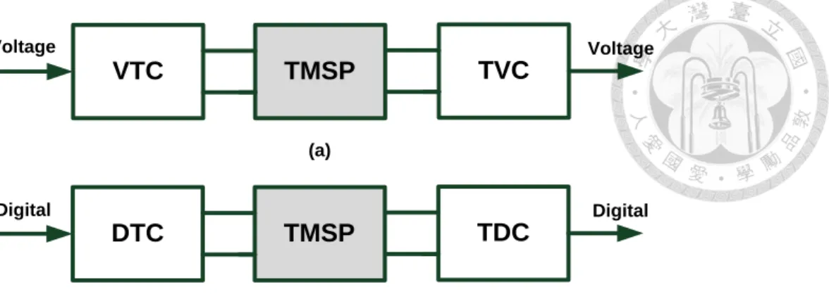
Roberts and Ali-Bakhshian [1] present a short review of time-to-digital and digital-to-time converters (TDCs and DTCs, respectively) adopting a time-mode signal processing perspective. Moreover, some mixed-mode circuits are used to convert non-time-domain signals to time-domain signals like input signals or output signals. In Fig. 1-1 (a), if the input is an analog voltage, it can be converted into a time-difference variable by a voltage-to-time converter (VTC). After the time-mode signal processing (TMSP) in the digital domain, the time-mode signal can be converted back to a voltage signal by a time-to-voltage converter (TVC). Here, the VTC and TVC are bridging circuits and the conversion process is very critical to ensure that the converted signal is reliable. Conversely, in Fig. 1-1 (b), if the input is a digital signal, it can be converted into a time difference variable as well by a DTC circuit. After some time-mode processing, it can be converted back into the original form using a TDC circuit. Similar to VTC and TVC, the TDC and DTC design are crucial to the whole system’s performance.
VTC TMSP
Voltage
TVC
Voltage
DTC TMSP TDC
Digital Digital
(a)
(b) VTC:Voltag-to-time converter TVC:Time-to-voltage converter DTC:Digital-to-time converter TDC:Time-to-digital converter
Figure 1-1 Time-Mode-Signal-Processing (TMSP) for processing analog and digital signals. (a) Voltage-in-voltage-out. (b) Digital-in-digital-out.
Due to the reasons described above, TMSP is becoming increasingly popular in several high-speed and moderate-accuracy analog circuits. For example, TDCs were used in all-digital phase-locked loops (ADPLLs) [2] and time-based analog-to-digital converters(ADCs) [3]-[6]. Again, a voltage-controlled oscillator (VCO) has been merged as a time-based quantizer in sigma-delta ADCs [7],[8]. It is a trend to convert an analog type signal to a time difference or a frequency difference signal, and then process the time domain signals using digital circuits. A growing number of published papers reporting such design in the time domain have demonstrated excellent performance compared to conventional designs in the voltage or current domain. Fig. 1-2 [7] shows a
VCO-based quantizer circuit and the relevant signal waveforms. The operation can be understood as follows. First, a ring oscillator converts a voltage signal Vtune to multi-phase clock outputs continuously. Next, the multi-phase clock signals are employed to trigger counters to start counting within a fixed clock period. After that, the counter outputs are summed and the results are saved to registers. The conversion is completed within a clock cycle and the counter is then reset before starting next conversion. If the output frequency of the ring oscillator is proportional to the input voltage Vtune, the analog voltage is successfully quantized to the relevant digital code in nature. A ring oscillator plus some digital counters and adders perform a
voltage-to-frequency conversion. The speed and accuracy of this quantizer take full advantage of modern CMOS processes since the ring oscillator’s gate delay and clock
phase spacing are reduced simultaneously with the process of scaling down. In addition, VCO-based quantizers can achieve first-order noise shaping of the quantization error.
Although the nonlinearity in the VCO’s transfer characteristic might seriously limit the resolution of VCO-based ADCs, sigma-delta feedback can be used to suppress the nonlinearity of the VCO quantizer. Consequently, VCO type quantizer has been widely adopted in continuous-time ΣΔ analog-to-digital converters. Fig. 1-3 is a proposed CT- sigma delta ADC. [7]
Figure 1-2 VCO employed as a quantizer [7]
Figure 1-3 The proposed CT-sigma delta ADC [7]
Another popular example of TMSP application is the all-digital PLL circuits employing TDC. Fig. 1-4 (a) shows a simplified block diagram of a charge pump based all-digital phase-locked loop (ADPLL) [9]. It consists of a phase-to-digital converter
(P2D), a digital loop filter, a digital controlled oscillator (DCO), and a feedback divider.
The P2D compares the phase difference between the reference clock FREF and the feedback clock FCKV, and converts it to a digital code. This digital code is filtered by the first-order digital low-pass filter (LF) and is then used to adjust the DCO’s phase or frequency. The P2D can be implemented as shown in Fig. 1-4 (b). It consists of a conventional phase/frequency detector (PFD) followed by a TDC. The PFD produces UP and DN pulses and the edge difference of UP and DN pulses is proportional to the phase error between the reference clock FREF and feedback clock FCKV. An L-bit TDC then digitizes the edge timing difference. The sign-bit of the TDC can also be generated according to the sampling results of the bottom D-flip flop. The operation of an ADPLL largely depends on the TDC resolution because it defines the resolution of PFD. A high-speed, high-accuracy TDC circuit (sub-gate delay resolution) design is often necessary in an ADPLL.
In Fig. 1-5, Lee et al. proposed a coarse-fine TDC design using an ADPLL [1]. It consists of an integer TDC and a sub-exponent TDC. The integer TDC is a conventional 5-bit TDC with one-bit resolution of two inverter delays. For the fractional time difference, a sub-exponent TDC to generate 1-of-n encoded 7b output with each bit representing a fraction 2-1,2-2,…,2-6,2-7 of the two inverter delay is used. The output of a
cascade of six stages of 2x time amplifiers (TAs) is tested by an integer checker. The
integer checker is a one-bit TDC and outputs ONE if the input time difference is larger than τ, which is equal to one bit resolution of the integer TDC.
(a)
(b)
Figure 1-4 All-digital phase-locked loop. (a) Block diagram. (b) A P2D converter. [9]
Figure 1-5 A coarse-fine TDC structure in all-digital phase-locked loop. [1]
1.2 Motivation and Research Goals
In this thesis, time mode circuits employed in two mixed-signal systems are presented and discussed. One is a high-speed time-based analog-to-digital converter system [37] and the other is an on-chip eye-opening measurement circuit for serial-link
receiver equalizer adaptations [47]. Our research goal is to move more analog circuits to digital domain for not only power and area saving but also more robust circuit design over PVT variations.
1.2.1 Time-Base ADC System
High speed and low-to-medium resolution analog-to-digital converters (ADCs) have been widely employed in all kinds of receiver front-end such as disk drive read channel, ultra-wideband, serial links or optical communication. In these applications, power efficiency and area occupancy are often critical issues since usually there are multiple channels on the same die. Flash type ADCs have the advantage due to their simplest and fastest property. However, in conventional designs, the voltage comparators and reference circuit like resistors ladders and voltage buffers always dominate the power consumption of the whole ADC system. Folding architectures have a merit of low power dissipation but suffers from is growing load capacitance of the folder circuits which is proportional to the required resolution. Time-interleaved multi-channel ADCs are often a doable structure when speed and power are trade-off but this architecture needs more precise clock phases for sampling.
In this thesis, a time-based ADC design is proposed. An analog input voltage-type
signal is converted to a time delay signal by a novel VTC circuit and the following flash TDC circuit then transfers this time delay to the corresponding digital code. Unlike conventional flash ADC designs, the comparator in the flash TDC is a time mode circuit like D-flip flops instead of voltage comparators. Voltage comparators often require a powerful preamplifier at its front end for amplifying a small analog signal to a logic level. The power consumption is always considerable to the whole ADC system.
1.2.2 Eye-Opening Monitor Circuit in Serial Link System
The purpose of an on-chip eye-opening monitor is to measure the eye quality information such as eye-height and eye-width of the received data before and after equalization in a serial link system. Due to the imperfect channel properties such as ISI, cross-talk, and reflection, continuous-time linear equalizer and decision feedback equalizer have widely been adopted in receiver front-end for signal equalizations.
In this thesis, a one-dimensional eye-opening monitor (1D-EOM) scheme with a novel multi-phase clock generator circuit is designed for wireline receiver front-end equalizer adaptations. The proposed multi-phase clock generator employs a simple VTC circuit without active or passive phase interpolation elements. It can provide 64 uniformly separated clock phases for sampling. For a Super Speed Universal Serial Bus
(SuperSpeed USB) (USB3.1 Generation 2, data rate is 10Gb/s) application, the sampling phase resolution is 1.5626ps. The presented 1D-EOM consumes less power and occupies a small layout area compared to those of a traditional EOM circuit.
Moreover, the measurement results show that the reported horizontal eye-opening value is proportional to the value from a real eye diagram monitor from the off-chip test buffer.
1.3 Dissertation Organizations
This dissertation is organized as follows. In chapter 2, several time mode circuits for analog and mixed-mode systems are introduced. In chapter 3, a time-domain ADC (TADC) is proposed. It consists of a delay-line-based VTC and a flash type TDC. The circuit implementation and chip measurements are also presented in this chapter. In chapter 4, an eye-opening monitor (EOM) circuit with a multi-phase clock generator is presented. A novel VTC circuit is included in this proposed EOM circuit. The VTC circuit can provide multi-phase clock outputs for EOM data sampling. The EOM circuit implementation and experimental results are also provided in this chapter. Finally, conclusion and discussions are given in chapter 5.
Chapter 2
Time Mode Circuit in Analog and Mixed-Signal Systems
2.1 Introduction
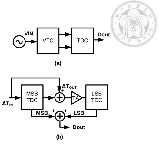
In chapter 1, several time mode signal processing circuits in time-based ADCs (TADCs) and all-digital PLLs (ADPLLs) are introduced. In this chapter, two critical building blocks in common TADCs, a voltage to time-difference converter (VTC) and a time difference amplifier (TA) are introduced and discussed, respectively. The VTC is used for voltage to time difference conversion and TA is used for time difference amplification. Figure 2-1 (a)(b) show their the application in mixed signal systems. In Fig. 2-1 (a), a VTC is employed in the front- end of a time-based ADC. In Fig. 2-1 (b), a TA is used in a two-step TDC for amplifying MSB’s residue. They are usually designed in pure analog circuits or some mixed-mode circuits. The performance of these two blocks will limit the speed and accuracy whole system. Due to this, some circuit design techniques and linearization methods in prior publications are also addressed in this
chapter.
VTC TDC
VIN Dout
MSBTDC - +
TA LSB
ΔTIN TDC
ΔTOUT
Dout LSB MSB
(a)
(b) + +
Figure 2-1 Time mode circuit in some mixed-signal systems. (a) VTC in the front-end of time-based ADC. (b) TA between two TDCs. Time mode circuit in mixed-mode system. (a) VTC in the front-end of time-based ADC. (b) TA between two TDCs.
2.2 Voltage-to-Time Difference Converter (VTC)
The voltage-to-time difference converter (VTC) is an interface circuit, transfer voltage information into time domain signals for time mode signal processing. The VTC operation is illustrated in Figs. 2-2 (a) and (b). It consists of two voltage-controlled delay units (VCDUs) and their inputs are differential voltage signals VIP and VIN. A test clock CKI input into two VCDUs and their output are delayed with respect to the
differential voltage, resulting in the rising edge difference between two VCDU’s output CKP and CKN. Assuming the two VCDUs are matched, we can write the edge difference as
∆T = (G × VIP + d0) − (G × VIN + d0) = G(VIP − VIN). (2.1)
Eq. (2.1) shows the output time variable ∆T of VTC that is linearly proportional to
the differential voltage input VIP minus VIN if the transfer gain of VCDUs is independent of input. G and d0 are the transfer gain and the intrinsic delay of VCDU.
The output time signals can be processed by some time mode circuits like TDC, TA…etc.
VCDU VIP
VCDU
VIN CKI
CKP
CKN CKP
CKN CKI
GVIP+d0
GVIN+d0
(a) (b)
∆T
Figure 2-2 Illustrations of voltage-to-time difference conversion. (a) Block diagram (b) Timing diagram
2.2.1 Linearization of VTC circuit
The linearity of VTC circuit will limit the input dynamic range of whole system.
For example, if it is employed in the front-end of time-based ADC, its nonlinear behavior will degrade the overall ADC’s performance. Due to this, several linearization methods have been proposed with an aim to enhance the linearity of the conversion. In [10] and [11], a delay-line-based ADC is proposed. Figure 2-3 (a) shows the circuit structure. It consists of a sample and hold circuit (S/H), a delay adjustment (DA) circuit and a delay-line based TDC.
A front-end S/H circuit samples the voltage input and then holds and converts it to a corresponding current signal by a degenerated differential pair amplifier DA as shown in Figure 2-3 (b) right side. The DA will output two current signals to discharge an initially pulled up capacitance in delay cells. The discharge rate is proportional to the current I over the capacitance C shown in Fig. 2.3 (c). To ensure linear conversion, the transconductance of the input NMOS differential pair M1 and M2 should be designed sufficiently large.
The sample and hold circuit is shown in the left side of Fig. 2-3 (b). Its operation is described as follow. In the sampling phase (S1~S4 are closed and S5~S8 are open), the
differential input Vin+ and Vin- are sampled on the top of the capacitances Cs and their bottom of the capacitances are connected to Vcm. The voltage across the top capacitor Cs is Vin+ minus Vcm and the bottom one is Vin- minus Vcm. In the converting phase (S1~S4 are open and S5~S8 are closed), the differential holding voltages (Vin+—
Vcm and Vin-—
Vcm) are then converted to corresponding currents (generated by diode-connected NMOS M9 and PMOS M10) to control the discharge current in delay cells (both P-cells and N-cells). Fig. 2-3 (c) is the scheme of the complete delay cell.
The delay-line-based ADC is fabricated in 65nm CMOS. The measured INL and DNL are +0.78LSB/-0.83LSB and +0.54LSB/-0.38LSB and it achieves an SNDR of 20.4dB at 1.2GS/s. The reported FOM is 196fJ/conversion step without using any calibration.
(a)
(b)
(c)
Figure 2-3 The delay-line based data converter [10].
(a) Delay-line based A/D converter implementation.
(b) Sample and hold circuit followed by a voltage to current converter.
(c) Controllable delay cells. (P-Cells and N-Cells).
In [12], Pekau et al. proposed a current starved delay cell for voltage-to-time delay conversion. The detailed schematic is shown in Figure 2-4. Degeneration MOS (M7 and M8) and parallel staggered bias MOS (M9~M14) are combined in the discharge path of the delay cell in order to adjust its linearity. The presented VTC circuit can operate at high conversion speed but fine-tune of the staggered MOS device size is needed to obtain better linearity. This VTC is designed in a 0.13µm CMOS process and the simulation result shows the gain error is less than 2% over an input voltage range of 200mV. Input signals at frequencies up to 1GHz can be applied to the VTC without using a sample-and-hold circuit.
Figure 2-4 A current starved inverter with a degeneration cell and parallel bias devices [12].
2.2.2 VTC in time-based ADC
In [13], Taehwan et al. proposed a hybrid pipelined ADC which uses both voltage and time domain information. The proposed new VTC scheme employs a scalable, power-efficient, residue voltage amplifier with minimum dc gain in its first stage while maintaining high linearity. This scheme not only reduces the power consumption of the ADC but also relaxes the design trade-off of the amplifier in a low supply voltage deep sub-micron process without sacrificing bandwidth. Figure 2-5 (a) is the proposed time-based pipelined ADC and Fig. 2-5 (b) and (c) are the conventional V-T conversion and the proposed new V-T conversion [13].
A conventional V-T conversion employed in noise-shaped two-step integration quantizer is shown in Fig. 2-5(b). The two-phase conversion results in the residue output in voltage domain after the amplification phase and is given by
𝑉𝑜= 𝐶𝑆
𝐶𝐹(𝑉𝐼𝑁− 𝑉𝑅) 𝐴
1 + 𝐴𝛽−𝐼𝐷𝐼𝑆𝑇𝑜
𝐶𝐹 . (2.2)
Where A is the open loop dc gain of the amplifier and β is the feedback factor
which is equal to 𝐶𝐹⁄(𝐶𝑆+ 𝐶𝐹). The amplifier gain is not a constant and is affected by
the output swing. Solving Eq. (2.2) , the time-domain output TO at zero crossing is
𝑇𝑜= 𝐶𝑆
𝐼𝐷𝐼𝑆(𝑉𝐼𝑁− 𝑉𝑅) 𝐴
1 + 𝐴𝛽 . (2.3)
(a)
(b)
(c)
Figure 2-5 Time based pipelined ADC [13]. (a) Time based pipelined ADC implementation. (b) Conventional voltage-to-time conversion. (c) Proposed voltage-to-time conversion.
According to Eq. (2.3), a nonlinear error from the amplifier directly affects the time-domain output. Fig. 2-5 (c) shows the proposed three-phase V-to-T conversion.
The charge stored in both sampling and feedback capacitors is discharged together.
There is no charge loss on both capacitors and discharged together to measure the time of zero crossing. The residue output after the amplification phase is
𝑉𝑜= [𝐶𝑆
𝐶𝐹(𝑉𝐼𝑁− 𝑉𝑅) −𝐼𝐷𝐼𝑆𝑇𝑜 𝐶𝐹 ] 𝐴
1 + 𝐴𝛽 . (2.4)
The residue output in voltage domain is still affected by the amplifier characteristics. However, the time-domain output at zero crossing in the discharge phase is independent of the amplifier dc gain A and given by
𝑇𝑜= 𝐶𝑆
𝐼𝐷𝐼𝑆(𝑉𝐼𝑁− 𝑉𝑅) . (2.5)
As a result, the time-domain output TO is regardless of the amplifier characteristics in the proposed V-T conversion. Therefore, a low gain nonlinear amplifier can be used. Fig. 2-6 shows the linearity simulation using a residue amplifier with 24 dB open loop gain.
Figure 2-6 Linearity simulation of the proposed V-T conversion [13].
2.3 Time Difference Amplifier (TA)
Low power and high resolution time-to-digital converters (TDCs) [14]-[16] have been widely used in mixed-signal circuits such as all-digital PLL (ADPLL) [17], time-domain analog-to-digital converters (ADCs) [18] - [21] and on-chip time measurement circuits [22]. To recognize a sub-gate delay time-difference signal, time-difference amplifier (TAMP) circuits have been developed in the front-ends of some TDCs to amplify a small time-difference signal. As shown in Figure 2-7, A TAMP can amplify a small time difference ∆Фin to ∆Фout, and ∆Фout is then fed into a LR-TDC (Low Resolution TDC) , it relaxes the resolution on TDC. Several type TAs are introduced in this section.
Figure 2-7 Time amplification relaxes resolution on TDC. [22]
2.3.1 SR-Latch-type Time-Difference Amplifiers [23]
Set/reset (SR)–latch-type time-difference amplifiers [23]-[25] operating in the metastable region can amplify a very small time-difference signal (of a picosecond or sub-picosecond scale) to a sufficiently large time-difference signal (of a scale of several picoseconds). The TA was designed to facilitate improvement of TDC resolution.
However, its linear range and metastable region are correlated.
The detailed circuit is presented in Figure 2-8 and relevant waveforms for inputs with small and large time-differences are presented in Figs. 2-9 (a) and (b), respectively.
As shown in Fig. 2-9 (a), for a small input time-difference of TD between INA and INB, the delay between A6 and B2 is TOS − TD and that between A2 and B6 is TOS + TD, where TOS is the time difference between INA and A6 (or INB and B6). The difference in the metastable time for LA1 and LB1 results in the doubling of the output delay between YP and YN. However, as shown in Fig. 2-9 (b), for input signals with a large time difference (TD–TOS), the delay between A6 and B2 is extremely small, resulting in a longer settling time for LA1. Consequently, the output time difference is over-amplified. As shown in Fig. 2-9 (b), the magnification ratio increases from 2 to 2.875.
INA
INB
YP
YN INA
A6
B2
A2 B6
LA1
LA2
LB1
LB2 C
C
C
C
...
x2 x6 INB
x2
...
x6
Figure 2-8 SR-latch-type TA schematic diagram.
INA INB A6 B2 A2 B6 LA1 LB1 LA2 LB2 YN YP
Tos+TD Tos-TD TD
2*TD TD
INA INB A6 B2 A2 B6 LA1 LB1 LA2 LB2 YN YP
TD
Tos-TD
Tos+TD
Td
2.875*TD
(a) (b)
Figure 2-9 Operating principles for input signals with (a) a small time difference (TD<<TOS) and (b) a large time difference (TD≈TOS) .
2.3.2 Dependent Discharge Time-Difference Amplifier [2]
In [2], a dependent discharge time-difference amplifier is proposed which uses a cross-coupled circuit structure to get a gain of two. A simplified schematic is shown in Figure 2-10. Initially, node A and B are precharged to VDD when IN+ and IN- are low.
OUT+ and OUT- are kept low and waiting for low to high transitions of IN+ and IN-.
When IN+ or IN- rising edge occur, node A or B start to be discharged and the discharging is performed by self-inverter path (M1 or M3) and a dependent path (M2 or M4). The strength of one dependent path is determined by the discharging status of the counterpart node (M2 gate is controlled by node B and M4 gate is controlled by node A).
The first transition makes the other transition slower by reducing the strength of the dependent path, resulting in an amplified time difference. Assume M1-M4 are identical, the first discharging is performed by two identical pull-down paths but the second discharging is performed by only one pull-down path. Therefore, the gain is roughly two when the IN+ and IN- rising edge are closed.
Figure 2-10 2X cross-coupled TA [2]
2.3.3 Pulse-Train Based Time-Difference Amplifier [26]
The principle of the pulse-train based TA is illustrated in Fig. 2-11[26]. The idea is to generate N copies of pulses with the same pulse-width of Tin. It can be equivalent to a wider pulse with a pulse-width N×Tin. Since the N input pulses of OR gate cannot be overlapping, the buffer delay time 𝜏𝑑 in the delay chain should be longer than pulse-width Tin. This results in limiting the TA speed. In addition, the balanced rise time and fall time of each buffer is necessary in order to maintain the same pulse-width on N inputs of OR gate. The input switches of OR gate determine the number of pulses that goes into the OR gate and thus controls the gain.
Figure 2-11 Pulse-train based TA [26]
2.3.4 Closed Loop Controlled Time-Difference Amplifier [27]
In [27], a time difference amplifier whose gain is controlled by a closed loop is proposed. The principle of the proposed TA is illustrated in Fig. 2-12. The delay time of each delay cell is variable and can be changed by a control pin. In Fig. 2-12 (b), the delay time is 4:1 when the control signal is H:L. The connection of two cross-coupled delay chains is shown in Fig. 2-12 (a). Every delay cell output is used to control the delay time in another cross-coupled delay chain. When the rising edge pass through a delay cell, then the output goes high and another cross-coupled cell’s delay time will become 4. For example, if the rising edge difference between in1 and in2 is 2 initially, they start to pass through the different delay chain respectively. In1 is from the left side to the right side and in2 is from the right side to the left side. Their rising edges will
meet in where the bold arrows point. Then the delay time of all delay cells are frozen.
The rising edge of in1 travel 5 delay cells and switch 5 delay cells to ―H‖ in the bottom
delay chain. The rising edge of in2 travel 3 delay cells and switch 3 delay cells to ―H‖ in the top delay chain. Eventually, the output rising edge difference between out1 and out2 is 8 which is amplified by 4.
Fig. 2-13 shows a block diagram of the proposed closed loop control TA. A
delay-locked loop (DLL) is employed to adjust the delay ratio of the variable delay cell with its delay switch of H/L to be 4. When the loop is locked, the delay ratio of the replica delay cell with its delay ratio H/L is adjusted to be 4, and the Vctrl is used to control the main delay cell of the cross-coupled delay chains.
Figure 2-12 Basic idea of the proposed TA in [27]. (a) Cross coupled chains. (b) Variable delay cell (c) Timing diagram.
Figure 2-13 TA using DLL-like closed-loop control. [27]
2.4 Summary
Delay-lined-based analog to digital converter is suitable for high speed and low power applications since the time mode circuit can usually be implemented in the digital domain and is of great benefit to the process migration. The most important time mode circuits, VTC and TA are introduced and some state-of-the-art designs are presented as
well in this section. VTC is usually used as the first stage of TADC. Its speed and accuracy directly limit the TADC’s performance. TA is a time domain amplifier. It is
often employed in a high-accuracy TDC for effectively amplifying the time residue. The amplifier gain linearity will affect the overall TDC’s resolution.
Chapter 3
A Time-Based Flash ADC
3.1 Introduction
Recently, picosecond or sub-picosecond resolution time-to-digital converters have been published [28]-[31]. These TDCs were developed using advances in processing technology and downscaling power supply voltages. Time-domain signal processing is becoming increasingly popular in high-speed and moderate-accuracy analog circuits.
High-speed and low-supply voltage demanding designs facilitate developing time mode circuit and processing time information.
In this chapter, time-based analog-to-digital converters (TADCs) are introduced.
These TADCs have achieved high performance, as reported in [10],[11] and [32],[33] . Among them, [10] and [11] are based on delay lines, whereas [32] and [33] are based on voltage-controlled oscillator. In addition, some voltage-domain ADCs also use auxiliary time-domain signal processing circuits to meet low supply voltage and low power consumption requirements; for example, in [34], Agnes et al. proposed a time-domain
comparator in a voltage-mode successive approximation register ADC, and in [13], Oh et al. proposed a mixed-mode ADC, in which the first stage was a voltage-type flash ADC. It converted the most significant bits and concurrently transferred the residue signal to the time domain through a three-step integration quantizer. The subsequent stage is a pipelined TDC, used to convert the time-domain residue to the least significant bits (LSBs).
Figure 3-1 depicts a delay-line-based ADC circuit approach. PH1 and PH2 are two out-of-phase clocks. At the sampling phase (PH1), the sample-and-hold circuit samples the voltage-mode signal and all delay cell outputs are reset to 0. At the evaluation phase (PH2), the sampled signal, Vc, is used to tune the delay time of the inverter chain, and a short-duration test pulse is injected into the delay chains and flip-flops simultaneously.
The test pulse travels down these inverters during PH2. The sampling flip-flops produce a thermometer code such as ―1….1100..0‖; the number of ones is the number of
inverters that have been visited, and should be proportional to the sampling voltage. The advantage of this structure is that it is simple and easy to implement. However, this ADC structure suffers from a tradeoff between speed and resolution. Higher resolution results in longer latency because of the intrinsic delay of the inverter chains. In addition, the linearity of the inverter chains is a bottleneck in these types of ADCs if no auxiliary
calibration circuit is included. Based on these considerations, such structure ADC is not suitable for high-speed and moderate-accuracy applications, unless more advanced processes are used. However, low supply voltage used in advanced processes may limit the dynamic range of traditional voltage-control delay cells.
This chapter is organized as follow. The operation principle of the proposed time-domain flash ADC is described in Section II. After that, the VTC implementations and simulation results are shown in Section III. Section IV is the flash TDC implementations. Then, the experimental results and summary are addressed in Section V and VI, respectively.
D(Vc)
D Q
Sample and Hold
PH1 PH2
D Q D Q
VDD
D Q D Q
IN OUT
Q[0] Q[1] Q[2] Q[N-3] Q[N-2] Q[N-1]
D(Vc) D(Vc) D(Vc)
PH1 PH2 Test pulse
D(Vc)
Vc Y=0
Figure 3-1 Basic structure of a delay-line-based ADC.
3.2 Proposed Time Domain Flash ADC [37]
In this Section, we will propose a time based ADC design example. The target ADC design is for high-speed (>100MHz), moderate-resolution (4~7 bits) and low power consumption (<10mA) applications. Moving amounts of analog circuits to digital domain is the target of high speed and low power dissipation.
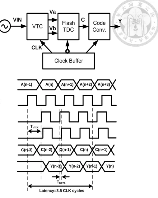
The proposed TADC performs a delay-based signal quantization [10]. That is, the sampling time is independent of input and the delay time is changed according to the analog input. Figure 3-2 shows the block diagram of our proposed TADC. The first stage is a voltage-to-time-difference converter (VTC). The voltage-domain input signal VIN is converted to two clocks Va and Vb outputs that are delayed signals with respect to a reference clock CLK. Their rising edge difference is proportional to VIN. The proposed VTC contains no sample-and-hold circuit because the overall intrinsic delay of the delay chain is much smaller than the sampling time. Therefore, the VIN change is a little bit when clock rising edge travels from the first stage to the last stage of the delay chain. It can be guaranteed by VTC dynamic simulation shown in Fig. 3-15.
The rising edge difference information is then transparent to the subsequent stage, a flash-type TDC. The flash type TDC output is 1-of-n code and can be periodically
sampled by an n-bits sampler with a constant sample time Ts. The last stage is a code conversion block. The purpose is to transfer 1-of-n code to binary code.
The TADC timing diagram is shown in Figure 3-2. VIN is an analog input. Va and Vb are defined as VTC clock outputs. The time skew between them is linearly proportional to VIN. The latency of the VTC should be shorter than a clock cycle. In this design, latency is 0.5 to 1 clock cycles. The flash TDC output C is a 32-bit 1-of-n code.
Y is a 5-bit binary output that is generated by the code conversion block. The clock signal is also used as a reference clock for VTC delay cell input. The falling edge of the clock is used to capture the flash TDC results simultaneously. Subsequently, the code conversion circuit transfers the 1-of-n code into Gray code synchronized by the clock rising edge. Finally, the Gray code outputs are converted to binary code and synchronized again by the clock rising edge. Thus, the total ADC latency is 3.5 clock cycles.
VTC Flash
TDC Code
Conv.
Clock Buffer VIN
Va
Vb
C Y
CLK
Va
Vb
CLK
VIN A(n-1) A(n) A(n+1)
C(n-2) C(n-1)
C C(n)
Y Y(n-3) Y(n-2) Y(n-1)
C(n-3)
A(n+2)
TVTDC
TDATA
A(n+3)
C(n+1)
Y(n)
Latency=3.5 CLK cycles
Figure 3-2 Block diagram of the proposed TADC and the relevant timing diagram.
3.3 Implementations of VTC
The principle and prior designs of VTC are also introduced in chapter 2. In this section, a delay-lined based VTC circuit is proposed for voltage-to-time conversion in the first stage of TADC [35][37]. In order to achieve high speed and high accuracy operation, the design and layout of some critical devices should be taken into account
carefully. In this section, the corresponding design equations and post-layout simulation results are provided to demonstrate its function. Section 3.3.1 addresses the VTC circuit operating principle and design considerations. Some non-ideal effects in an imperfect circuit are also discussed. The simulation results are described in section 3.3.2.
3.3.1 VTC design [35]
The proposed VTC consists of a load control circuit, VREF generator, dual path delay chains and a phase detector. The block diagram was depicted in Figure 3-3 (a).A load control circuit can be divided into a load tuning circuit and two delay replica-biasing circuits. The load tuning circuit converts the input signal VIN to a differential signals Vctrlp and Vctrln are the inputs of two delay replica bias. The delay replica bias circuit will control the output swing of the replica delay cell by a negative feedback and then generate two pairs bias voltages Vcsp(Vcsn) and Vbnp(Vbnn) for the real delay cells (DPx and DNx) biasing. Figure 3-3 (b) shows the corresponding waveforms of VTC.
Load Control
DP1 DP2 DP6
DN1 DN2 DN6
Slicer
Slicer
BUF Phase
Detector
Lead/Lag CKPd/CKNd Analog
Input
Sampling
clock CKP
CKN Vcsp Vbnp
VbnnVcsn
Load Tuning
Delay Replica
Bias Delay Replica
Bias Vctrlp
Vctrln
Vcsp
Vbnp Vcsn
Vbnn +
_ VIN
Vcsp Vbnp
Vcsn Vbnn VREF Gen.
CK
VIN
(a)
CKP CK
CKN VIN
t=n
t=n-1 t=n+1
-∆T ∆T
(b)
Figure 3-3 (a) Proposed VTC block diagram. (b) VTC output waveform.
The operation is described below. If Vctrlp is greater than Vctrln, the clock edge of CKP will lead CKN. In contrast, if Vctrln is greater than Vctrlnp, the result is inversed.
Since the transfer curve of the delay time versus the control voltage is nonlinear, a load
tuning circuit is needed for correcting this non-linearity. The delay replica bias circuit contains a replica of the delay cell, which controls the bias of the delay cell in order to force its output voltage to be clamped between 0 and Vctrlp,n. The dual path delay chain propagates the reference clock CK with a relevant delay time according to the delay control signals Vcsp,Vcsn,Vbnp and Vbnn. The delay chain output signals CKP and CKN have differential time difference properties and the waveforms shown in Figure 3-3 (b).
The purpose of the phase detector is to detect the VTC output signal in advance.
The lead (or lag) flag indicates the polarity of analog input. It facilitates preventing the VTC outputs from unnecessarily entering some comparator units of the subsequent flash TDC, thereby markedly reducing power consumption. Only two thirds of the comparator units are toggled during each code conversion. CKPd and CKNd are the delayed signals with respect to CKP and CKN for compensating the latency of the phase detector. The phase detector circuit was implemented using a D-Flip-Flop.
The proposed load tuning circuit is shown in Figure 3-4 (a).The NMOS input degenerated differential pair (MN3 and MN4) with a PMOS diode connected load (MP2~MP5) converts the input differential signals VP and VN into a differential delay control voltages Vctrlp and Vctrln. The PMOS diode connected load is used to match
the symmetric load of the delay cell in the dual path delay chain.
The delay cell with a symmetric load is proposed in [36]. It has a very broad delay range but the delay time is nonlinear with respect to the control voltage. In fact, the delay changes proportionally to 1/(VCTRL-VT), where VCTRL is control voltage of the symmetric delay cell and VT is the threshold voltage of the diode connected load (In our design is NMOS MNL1~MNL4 shown in Fig. 3-6 (a).). The transfer curve of delay time versus control voltage, VCTRL is shown in Figure 3-5 (a). Figure 3-5(a) also shows that the characteristic curve will shift due to different process corners. This offset will limit the input dynamic range and overload the following TDCs as well. In order to mitigate this effect, a VREF generator circuit has been added as shown in the Figure 3-4 (b). The purpose is to sense NMOS MN1 and PMOS MP1 threshold voltage and then amplify the summation of their threshold voltage (Vx) by (1+R2/R1). VREF serves as the supply voltage of the diode connected load (MP2~MP5) and the output source follower circuit (MP7 and MP8 are input transistors) which is shown in Figure 3-4 (b). At slow P and slow N corners, the PMOS and NMOS will have a higher threshold voltage. This implies that VX and VREF are also higher and will shift the delay control voltage Vctrlp and Vctrln to a higher level in order to compensate the lower speed of delay cell. Eq.
(3.3) is the design equation of VTC transfer gain. This compensation can be
demonstrated roughly using this equation. Figure 3-5 (a) and (b) show the illustrations of uncompensated and compensated VTC transfer curve. The output time variable is defined as the rising edge difference between the two delay chains output, CKP and CKN, and it can be derived as follows:
∵ ∆𝑇𝑃,𝑁∝ 𝐶
𝑔𝑚,𝑑𝑒𝑙𝑎𝑦 𝑓𝑜𝑟 𝑎𝑙𝑙 𝑑𝑒𝑙𝑎𝑦 𝑐𝑒𝑙𝑙𝑠,
∴ ∆𝑇 = 𝐾𝑁 × (∆𝑇𝑃 − ∆𝑇𝑁) = 𝐾 ( 𝐶 2𝐾⁄ 𝑁
𝑉𝐶𝑇𝑅𝐿𝑃− 𝑉𝑇𝑁𝐿− 𝐶 2𝐾⁄ 𝑁
𝑉𝐶𝑇𝑅𝐿𝑁− 𝑉𝑇𝑁𝐿) , and 𝑉𝐶𝑇𝑅𝐿𝑃 = 𝑉𝑅𝐸𝐹− 2𝑉𝑆𝐺𝑃 , + 𝑉𝑆𝐺𝑃 = 𝑉𝑅𝐸𝐹− 2 (|𝑉𝑇 , | + √(𝐼 + ∆𝐼) 𝐾⁄ ) + |𝑉𝑃 𝑇 | ,
𝑉𝐶𝑇𝑅𝐿𝑁= 𝑉𝑅𝐸𝐹− 2𝑉𝑆𝐺𝑃 , + 𝑉𝑆𝐺𝑃 = 𝑉𝑅𝐸𝐹− 2(|𝑉𝑇 , | + √(𝐼 − ∆𝐼) 𝐾⁄ ) + |𝑉𝑃 𝑇 | , 𝑉𝑅𝐸𝐹= (1 +𝑅 𝑅 ) (𝑉𝑆𝐺𝑃 + 𝑉𝐺𝑆𝑁 ) = (1 +𝑅 𝑅 ) (|𝑉𝑇𝑃 | + 𝑉𝑇𝑁 + √𝐼 ⁄𝐾𝑃 + √𝐼 ⁄𝐾𝑁 ),
(3.1)
∆T = KN(𝐶 2𝐾⁄ 𝑁)
(𝑉𝑅𝐸𝐹 − |𝑉𝑇|−𝑉𝑇𝑁𝐿) − √(𝐼 + ∆𝐼) 𝐾⁄ 𝑃− KN(𝐶 2𝐾⁄ 𝑁)
(𝑉𝑅𝐸𝐹− |𝑉𝑇|−𝑉𝑇𝑁𝐿) − √(𝐼 − ∆𝐼) 𝐾⁄ 𝑃
= KN(𝐶 2𝐾⁄ 𝑁)(√(𝐼 + ∆𝐼) 𝐾⁄ 𝑃− √(𝐼 − ∆𝐼) 𝐾⁄ )𝑃
*((𝑉𝑅𝐸𝐹 − |𝑉𝑇|−𝑉𝑇𝑁𝐿) − √(𝐼 + ∆𝐼) 𝐾⁄ ) ((𝑉𝑃 𝑅𝐸𝐹 − |𝑉𝑇|−𝑉𝑇𝑁𝐿) − √(𝐼 − ∆𝐼) 𝐾⁄ )+𝑃
≈ √ 𝐼 𝐾𝑃×
(KNC
2𝐾𝑁) *(1 +1 2 (ΔI
I ) −1 4 (ΔI
I ) ± ⋯ ) − (1 −1 2 (ΔI
I ) −1 4 (ΔI
I ) ± ⋯ )+
[(𝑉𝑅𝐸𝐹− |𝑉𝑇|−𝑉𝑇𝑁𝐿) − √𝐼 𝐾⁄ ]𝑃
≈ √ 1
𝐾𝑃𝐼× (KNC
2𝐾𝑁) ∆𝐼
[(𝑉𝑅𝐸𝐹 − |𝑉𝑇|−𝑉𝑇𝑁𝐿) − √𝐼 𝐾⁄ ]𝑃
≈ √ 1
𝐾𝑃𝐼× (KNC
2𝐾𝑁) (∆𝑉𝐼𝑁 R )
[(𝑉𝑅𝐸𝐹 − |𝑉𝑇|−𝑉𝑇𝑁𝐿) − √𝐼 𝐾⁄ ]𝑃 (3.2)
Where ΔTP and ΔTN are absolute delays of the two delay cells DPx and DNx,
respectively. VCTRLP and VCTRLN are the control voltage of P-side and N-side delay cells, N is the total number of delay cells in one delay chain, KP and KN are the current gain of PMOS diode connected load (MP2~MP5) in Figure 3-4 (b) and NMOS symmetrical load of delay cell (MNL1~MNL4) in Figure 3-6 (a). C is the output capacitance of all
delay cells and K is a constant. 𝑉𝑇𝑁𝐿 is the threshold voltage of the NMOS symmetric load. |𝑉𝑇𝑃 | and 𝑉𝑇𝑁 are the threshold voltage of MP1 and MN1 in VREF generator
circuit in Figure 3-4 (a) and IB is their bias current. |𝑉𝑇 , |, |𝑉𝑇 , |, |𝑉𝑇 |and |𝑉𝑇 | are the threshold voltage of PMOS devices MP2,MP3,MP4,MP5,MP7 and MP8 in load
tuning circuit. To simplify this derivation, assume they are identical, and the threshold voltage is defined as|𝑉𝑇|. By Eq. (3.1) and (3.2), the overall gain of VTC can be
expressed as G, and
G = ( ∆T
∆𝑉𝐼𝑁)
![Figure 1-5 A coarse-fine TDC structure in all-digital phase-locked loop. [1]](https://thumb-ap.123doks.com/thumbv2/9libinfo/9604121.630357/24.892.191.771.124.700/figure-coarse-fine-tdc-structure-digital-phase-locked.webp)
![Figure 2-3 The delay-line based data converter [10].](https://thumb-ap.123doks.com/thumbv2/9libinfo/9604121.630357/33.892.236.783.118.829/figure-delay-line-based-data-converter.webp)
![Figure 2-4 A current starved inverter with a degeneration cell and parallel bias devices [12]](https://thumb-ap.123doks.com/thumbv2/9libinfo/9604121.630357/34.892.138.754.674.907/figure-current-starved-inverter-degeneration-cell-parallel-devices.webp)
![Figure 2-5 Time based pipelined ADC [13]. (a) Time based pipelined ADC implementation](https://thumb-ap.123doks.com/thumbv2/9libinfo/9604121.630357/37.892.238.783.119.532/figure-time-based-pipelined-time-based-pipelined-implementation.webp)
![Figure 2-11 Pulse-train based TA [26]](https://thumb-ap.123doks.com/thumbv2/9libinfo/9604121.630357/43.892.166.734.734.984/figure-pulse-train-based-ta.webp)
![Figure 2-12 Basic idea of the proposed TA in [27]. (a) Cross coupled chains](https://thumb-ap.123doks.com/thumbv2/9libinfo/9604121.630357/45.892.183.713.428.761/figure-basic-idea-proposed-ta-cross-coupled-chains.webp)
![Figure 2-13 TA using DLL-like closed-loop control. [27]](https://thumb-ap.123doks.com/thumbv2/9libinfo/9604121.630357/46.892.203.784.118.405/figure-ta-using-dll-like-closed-loop-control.webp)