國立交通大學
電子工程學系 電子研究所碩士班
碩 士 論 文
射頻功率偵測器的應用
Applications of RF Power Detectors
研究生:謝易耕
指導教授:郭建男 教授
中 華 民 國 九十七 年 七月
射頻功率偵測器的應用
Applications of RF Power Detectors
研究生: 謝易耕 Student: Yi-Keng Hsieh
指導教授: 郭建男 Advisor: Chien-Nan Kuo
國立交通大學
電子工程學系 電子研究所碩士班
碩士論文
A Thesis
Submitted to Department of Electronics of Engineering & Institute of Electronics College of Electrical Engineering and Computer Engineering
National Chiao Tung University In Partial Fulfillment of the Requirements
For the Degree of Master
In
Electronic Engineering July 2008
Hsinchu, Taiwan, Republic of China
中華民國 九十七年 七月
射頻功率偵測器的應用
學生 : 謝易耕 指導教授 : 郭建男 教授
國立交通大學
電子工程學系 電子研究所碩士班
摘要
本論文提出兩個射頻功率偵測器的應用電路。主要是利用現有的射頻電路架 構搭配一些功能性的類比電路,而以功率比較的方式達成射頻偵測的目的。第一 個電路應用在WiMAX 傳送端上。為了能完成 I/Q 自動校正的閉迴路系統,一個 具 有 較 寬 動 態 範 圍 的 射 頻 功 率 偵 測 電 路 是 必 須 的 。 此 電 路 使 用 了 台 積 電 0.18um,而模擬結果顯示在本地振盪器漏訊號,IQ 增益及相位誤差補償模式下 都符合規格要求。 另一個應用則是5GHz 低雜訊放大器的自我測試電路。偵測待側電路增益的 方法是以可調整式衰減器及兩個射頻功率偵測器的輸出進行比較的方式達成。後 模擬結果顯示,可以完成一個增益為15.68dB 的低雜訊放大器的偵測。不幸地, 因為天線效應的影響,量測沒辦法和模擬結果相互驗證。之後,提出另一個自我 測試電路的架構,主要是以電阻分壓的方式來克服對溫度及製程變異的影響。 IApplications of RF power detector
Student : Yi-Keng Hsieh Advisor : Chien-Nan Kuo
Department of Electronics Engineering & Institute of
Electronics
National Chiao-Tung University
ABSTRACT
In this thesis, two applications of RF power detector are designed using power comparing methodology as a design principle. The first application is the power detection design in WiMAX transmitter. In order to form a closed loop I/Q auto-calibrated system, a wide dynamic range power and detection circuit is necessary. Simulations results show that the power detection circuitry designed in TSMC 0.18um technology meets the specifications in all compensation mode, such as LO feedthrough, gain imbalance, and phase imbalance.
Another application of RF power detector is the built-in self-test design for a 5GHz LNA. The circuit under test is test by a variable attenuator and comparing the DC output of the power detectors. The post-simulation results show that the circuit achieves gain test for a 15.68dB, 5GHz LNA. Unfortunately, function verifications cannot be made due violations of the antenna rule. Another BIST architecture using voltage division by a resistor string is also proposed to break-through the bottlenecks of sensitive to process and temperature variations.
誌謝
能夠完成畢業論文,順利取得碩士學位,要感謝的人真的很多。首先是,我 的父母親,能夠提供我一個沒有經濟負擔的環境一路往上念,並且適時關心我, 並鼓勵我繼而攻讀博士學位。再來,我要對我的指導教授至上誠摯的感謝。這兩 年來,不僅提供了良好的研究環境與設備,並且讓我對射頻及類比電路的領域有 深層的了解。適時的指點迷津,讓我學習到有邏輯的分析方法與嚴謹的研究態 度。此外我要對昶綜與宗男兩位學長致上萬分的謝意,除了教導我許多軟體與硬 體上的使用,也時常分享寶貴的研究與人生經驗,讓我一直有學習的好榜樣。 感謝實驗室的其他學長姐,俊興、燕霖、淑惠、明清、鴻源、鈞琳、培翔等 的不吝指教與技術支援。感謝一起奮鬥一起研究的好同學,煥昇,以及建忠、子 超、俊豪、信宇、俊毅、瑋琪、佑偉、宇航等學弟,你們使實驗室不再是一個無 聊的地方。 最後感謝女朋友詠文從大學一直到研究所的陪伴,謝謝你在這兩年碩士生活 中陪伴我走過許多人生的起起伏伏。在我研究上遇到瓶頸時,你的鼓勵與支持讓 我走過種種一切的不如意;在我忙碌於研究時,你總是默默的陪伴在我身邊替我 加油,讓我能無後顧之憂的向成功邁進。 謝易耕 九十七年 七月 IIICONTENTS
Abstract (Chinese)………I
Abstract (English)………II
Acknowledgments………..….III
Contents………IV
Table Captions………VII
Figure Captions………VIII
Chapter I
Introduction………1
1.1 Motivation………...1
1.2 Thesis Organization………1
Chapter II Fundamentals of RF detection circuits………2
2.1 Introduction……….2
2.2 Meyer power detector……….3
2.3 Logarithmic amplifier……….9
Chapter III RF power detection circuit design in WiMAX
transmitter………..16
3.1 Motivation………16
3.2 RF power detection circuit design………....20
3.2.1 Input buffer………...21
3.2.2 Pre-amplifier………22
3.2.3 Meyer power detector & PD buffer……….……….23
3.2.4 Comparator………...……26
3.3 Simulation results……….30
3.4 Chip layout & summary………31
Chapter IV Built-in self-test circuit designs for 5GHz LNA
4.1 Introduction………33
4.2 RF BIST design with a digital step attenuator………..34
4.2.1 The BIST architecture………....34
4.2.2 Low noise amplifier……….37
4.2.3 Switch A………...37
4.2.4 Power detector………38
4.2.5 Digital step attenuator………...43
4.2.6 Design guidelines of the DSA……….….47
4.2.7 Post simulation results………..48
4.2.8 Chip implementations and measurement………..53
4.3 RF BIST design with R-72R ladder………..…61
4.3.1 Variations of the DSA……….…….61
4.3.2 R-72R voltage attenuator……….64
4.3.3 R-72R ladder and power detector combination………...…66
4.3.4 Current amp PD with high input impedance………....69
4.3.5 Comparator………70
4.4 Summary……….…74
Chapter V Conclusion and Future Work
5.1 Conclusion………76
5.2 Future Work………..76
References………77
TABLE CAPTIONS
Table 1 Attenuation levels………...…….36 Table 2 Performance summary of the CUT in operating mode………51 Table 3 Compare with recent RF BIST designs………...75
FIGURE CAPTIONS
Fig. 2-1 Meyer power detector……….. 3
Fig. 2-2 Transfer curve of the Meyer power detector………6
Fig. 2-3 Frequency response of the Meyer power detector ………...8
Fig. 2-4 Logarithmic transfer curve………..11
Fig. 2-5 PN-junction based log amp……….12
Fig. 2-6 Principle diagram of successive detection logarithmic amplifier…………...14
Fig. 2-7 Behavior model simulation of a log amp………15
Fig .3-1 Direct up-conversion mixer with auto-calibration for I/Q imbalance and LO feedthrough………...18
Fig. 3-2 LO feedthrough of one side of the I/Q mixer’s output vs. control bits……….…...19
Fig. 3-3 The RF output signal of I/Q mixer’s during gain error test vs. control bits...20
Fig. 3-4 RF power detection architecture……….21
Fig. 3-5 Simulation of input matching……….22
Fig. 3-6 Simulation of the switching path………23
Fig. 3-7 Meyer PD transfer curve……….25
Fig. 3-8 PD buffer transfer curve……….25
Fig. 3-9 Simulation results of the circuits before comparator………..26
Fig. 3-10 Schematic of comparator………..27
Fig. 3-11 Timing of the comparator……….28
Fig. 3-12 Simulation results of the comparator………30
Fig. 3-13 Simulation results of gain error and LO feedthrough………...31
Fig. 3-14 Layout of the RF power detection circuit……….32
Fig. 4-1 Proposed BIST architecture………34 VIII
Fig. 4-2 Modes of the RF BIST………...35
Fig. 4-3 Circuit under test………37
Fig. 4-4 Switch A……….38
Fig. 4-5 PD characteristic curve………...38
Fig. 4-6 Power detectors………...40
Fig. 4-7 Time response with different input levels………...43
Fig. 4-8 Digital step attenuator……….44
Fig. 4-9 DSA check………..46
Fig. 4-10 Post simulation results of the CUT………...50
Fig. 4-11 Test mode………..52
Fig. 4-12 Die photo………..53
Fig. 4-13 Violations of antenna rule……….54
Fig. 4-14 Measurement results……….58
Fig. 4-15 P1dB measurements……….59
Fig. 4-16 Noise figure………..59
Fig. 4-17 Power detector curve measurement………..60
Fig. 4-18 Observation of process variations for the DSA………61
Fig. 4-19 27°C Simulation………...62
Fig. 4-20 55°C Simulation………...63
Fig. 4-21 R-72R Ladder………...65
Fig. 4-22 Simulation result of the R-72R ladder………..66
Fig. 4-23 Combination ideas………67
Fig. 4-24 High impedance power detector………...70
Fig. 4-25 Input offset cancellation………...71
Fig. 4-26 Schematic of the comparator………72
Fig. 4-27 Modified BIST architecture………73
Chapter I
Introduction
1.1
Motivation
A RF power detection circuit for auto-compensating I/Q mismatch and LO-feedthrough of the direct up-conversion mixer is necessary to form a closed-loop design in my senior’s project [1]. The first task was to design cascading stages of RF power detection circuits, including a pre-amplifier, a power detector, and a comparator, that can meet the specifications given. Some of the design backgrounds of RF power detection during this work is covered up. Furthermore, this motivates research topics on applications for the power detectors, such as built-in self test (BIST) designs for RF-circuits.
In this thesis, a RF BIST design using power comparing method instead of designing wide dynamic range and low error power detectors to test the gain of a low noise amplifier is described. Another work of modifying the original idea is also proposed to break-through the bottleneck of process variations.
1.2
Thesis organization
In Chapter II, some of the backgrounds of the RF detection techniques will be cover. In Section 2.1, basics of Meyer power detector along with its design equations are introduced. The successive detection theory of the logarithmic amplifier is written in Section 2.2. In Chapter III, the power detection circuit design in a WiMAX transmitter is introduced. In Chapter IV, BIST circuit designs for 5GHz LNA are described. Finally, some conclusion and future work is written in Chapter V
Chapter II
Fundamentals of RF detection circuits
2.1
Introduction
This chapter introduces some of the recent approaches of detecting RF signals. The surveyed publications can be categorized into two groups. One group is the circuits that detect RF signals directly and convert it into a DC value [2]-[12] which are able to work at frequencies GHz-frequencies, such as power detector, peak detector, amplitude detector, RMS detector, rectifier, etc.
The other one is the logarithmic amplifier (log amp) [13]-[20] that can convert a large dynamic range dB-linear input into small dynamic range linear output which usually works at MHz-frequencies. Logarithmic amplifiers are typically used in AGC-loops as RSSIs (received signal strength indicator) to detect the signal amplitude. Especially in communication systems, it is very important to know the incoming signal level accurately so that a reliable decision between a successful or a failed connection can be made. Also the required number of bits for the A/D-converter which is usually placed as the following circuit block can be more relaxed with an AGC amplifier. This implies that the dynamic range, accuracy, and process dependency are the major design challenges. Logarithmic amplifier can also be arranged as the succeeding stage of a power detector [10]-[12] (or the other detectors mentioned above) that compress the large dynamic range to a readable output during detection.
In Section 2.2, a popular Meyer power detector is analyzed by means of Taylor
series. In Section 2.3, an overview of the logarithmic amplifier is given.
2.2
Meyer power detector
A monolithic low power RF power detector using bipolar transistors (fT=8GHz)
was first invented by Meyer [2] in 1995. This detector can be used for embedded RFIC test because it has the advantages of simplicity, wide bandwidth, low power, small chip size, and temperature stability. The detector was also analyzed by Zhang using similar approach, such as Bessel function [3]. A modified design was also proposed to extend its dynamic range. The following will repeat their analysis by means of Taylor series and replace the bipolar transistors with MOSFET biased at sub-threshold region which the current is also expressed in exponential function.
Fig. 2-1 Meyer power detector
Fig. 2-1 is the schematic of a Meyer power detector (Meyer PD). M1 acts as the
nonlinear rectifying element on signal voltage Vi. Transistor M2 sets up a replica
circuit so that DC voltage VO(=VO+−V )O− is zero for zero AC signal input at Vi.
Notice that M1 and M2 are identical and are biased at their sub-threshold region. C1
and C2 are large enough to filter out the unwanted high frequency components and
generate a pure DC output as possible. VO can be expressed as:
2
( ) ( )
O O O X O X O GS GS
V =V +−V −= V −V − − V −V + =V −V 1 (2.1) The sub-threshold current of M1 can be expressed as:
1 1 0 1 0 1 0 2 3 4 1 0 exp[ ] ( ) exp[ ] exp[ ]*exp[ ] 1 1 1 exp[ ]*[1 ( ) ( ) ( ) ( ) ...] 2! 3! 4! GS THN D D T GS gs THN D T gs GS THN D T T gs gs gs gs GS THN D T T T T T v V W i I L nV V v V W I L nV v V V W I L nV nV v v v v V V W I L nV nV nV nV nV − = + − = − = − = + + + + + (2.2) 2 2 2 2 2 4
Set cos , where is the amplitude of the input signal and is the input frequency 1 cos 2
then, cos , there will be a DC term such as
2 2
Similarly, we can get: [
gs in in in gs in in gs in v V t V V t v V t V v V ω ω ω ω = + = =
= 21 cos 2 ] , and there will be a DC term such as 2 3 4
2 8 in V t ω +
So the DC term of iD1 will be:
2 4 2 4 1 0 3 1 1 1 1 exp[ ]*[1 ( ) ( ) +.. 2! 2 4! 8 GS THN in in D T T T V V V V W I L nV nV nV − + + .] (2.3) Since identical current sources are used, the equation can be written as:
1 2 2 4 2 4 1 2 0 0 2 4 2 4 2 1 3 1 1 1 1 exp[ ]*[1 ( ) ( ) +...] exp[ ] 2! 2 4! 8 3 1 1 1 1 [1 ( ) ( ) +...] exp[ ] 2! 2 4! 8 D D GS THN in in GS THN D D T T T in in GS GS T T T I I V V V V V V W W I I L nV nV nV L nV V V V V nV nV nV = − − ⇒ + + = − ⇒ + + = T (2.4) With (2.1) and (2.4) 2 4 2 4 3 1 1 1 1 *ln[1 ( ) ( ) +...] 2! 2 4! 8 in in o T T T V V V nV nV nV = + + (2.5) When Vin is small, VO can be approximated as:
2 2 2 1 1 *ln[1 ( ) ] 2! 2 4( ) in in o T T T V V V nV nV nV = + ≈ (2.6)
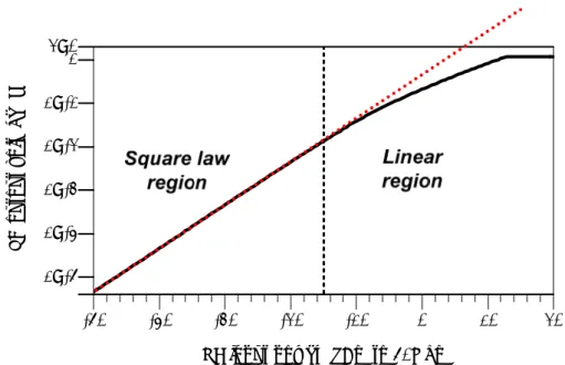
(2.6) shows that when the input signal is small, the differential DC output will be proportional to the square of the input signal amplitude and this is referred as the square law region of the power detector. Besides, it is apparent that the output is approximately inversely proportional to absolute temperature. Temperature could be compensated by dividing by a quantity proportional to temperature. Meyer also derived the equation for large Vin and the DC output can be expressed as:
2 ln in o in T T V V V V nV π = − (2.7) This can be approximated as a linear relation between VO and Vin.
We can conclude shortly that the power detector can work in the linear region for large signal detection and in square law region for small signal detection. Fig. 2-2 is a simulation of a Meyer PD using TSMC 0.18um technology to verify the mathematical derivation above. The transition power level of the linear and square law region is about -15dBm. The dynamic range is at least -35dB for the square law region and 25dB for the linear region. Notice that the output of Meyer PD is logarithmic linear.. A logarithmic amplifier can be added behind the PD to convert linear in dB input into linear output.
Instead of examining the Meyer PD by tedious mathematical equations, we can still use our “engineer’s intuition” to explain the mechanism. Re-visit Fig. 2-1 and assume that there isn’t any input signal. Hence, the VGS of both transistors will ideally
be the same since they are biased with identical current sources. While there is an input signal, M1 then adjusts its VGS to maintain the constant DC current. Since the
gate voltage of M1 is fixed, its source (VO+) will change proportionally to the strength
of the input. -40 -30 -20 -10 0 10 -50 20 1E-4 1E-3 1E-2 1E-1 1 1E-5 2E0
RF input power (dBm to 50Ohm)
P D out out vol ta ge ( V )
Fig. 2-2 Transfer curve of the Meyer power detector
In [3], an analysis of a periodic input signal of any shape instead of a pure sinusoidal is given. It shows that the possibilities of Meyer PD in multi-tone detections. The input periodic signal can be represented as the sum of N harmonics, where N is a positive integer.
, 1 cos( ) N i in i i i V V ωt θi = =
∑
+ (2.8) whereVin i, ,ω ,i θ are the amplitude, angular frequency, and phase of the ith harmonic. i Thus, the current of M1 can be expressed as:1 1 0 1 1 0 cos( ) , 1 0 1 exp[ ] exp[ ] GS THN D D T GS gs THN D T V t VGS VTHN N in i i i nVT nVT D i v V W i I L nV V v V W I L nV W I e e L ω θ+ − = − = + − = =
∏
(2.9) The equation above can be re-written in the form of Bessel functions [23].cos( ) , 1 1 0 1 1 0 0 1 2 1 [ ( ) 2 ( ) cos( ) 2 ( ) cos( ) ....] V t VGS VTHN N in i i i nVT nVT D D i VGS VTHN N nVT D i i i i i i i W i I e e L W I e I b I b t I b t L ω θ ω θ ω θ + − = − = = = + + + + +
∏
∏
i (2.10) where I b0( )i is modified Bessel function of n and i in i,T
V b
nV
= .
It is seen in (2.10) that each harmonic (ith harmonic) produces a DC component
0( )i
I b and other AC components. The total current depends on all of the harmonics.
Sinceω ωi ≠ j, ∀ ≠ , cross-modulation among them does not produce any DC i j component. Thus, the DC current component of iD1can be viewed as the result of DC
components produced by the corresponding harmonics. For small signal detection, where thebi'sare small,
2 0( ) 1 4 i i b I b ≅ + (2.11) Therefore, the DC current will be:
1 1 0 0 1 1 2 0 1 1 2 , 0 2 1 ( ( )) (1 ) 4 (1 ) 4( ) VGS VTHN N nVT D D i i VGS VTHN N i nVT D i VGS VTHN N in i nVT D i T W I I e I b L W b I e L V W I e L nV − = − = − = = = + =
∏
∏
∏
+ (2.12)Similarly, since identical DC current sources are used.
1 2 2 , 0 2 1 (1 ) 4( ) VGS VTHN VGS VTHN N in i nVT nVT D i T V W I e I e L nV L − − = + =
∏
D0 W (2.13) Combining (2.1) and (2.13), 72 , 2 1 2 1 2 , 1 ln(1 ) 4( ) 1 4 N in i o GS GS T i T N in i T i V V V V nV nV V nV = = = − = + ≅
∑
∑
(2.14)It shows that the output voltage is linearly proportional to the sum of the squares of all harmonics’ amplitudes, which corresponds to the total power. However, no mathematical analysis for the linear region is given in [3] any further. Maybe analysis for multi-tone large signal detection will be another interesting research topic in the future.
Fig. 2-3 Frequency response of the Meyer power detector
Fig. 2-3 shows that the Meyer PD can work in the GHz range. The low frequency response depends on the size of the loading capacitor.
2.3
Logarithmic amplifier
2.3.1
Ideal logarithmic transfer function
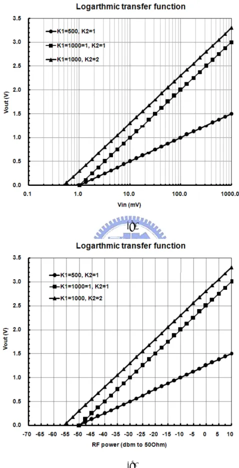
The general transfer function of a logarithmic amplifier can be given as [13]
1log 1log
out in
V = K V +K K2 (2.8)
where K1 and K2 are constants associated with the logarithmic amplifier. Fig. 2-2
shows the equation above graphically with three sets of K1 and K2. The design
parameter K2 can be solved by setting Vout =0
1 1 2 log log 1 in 2 in K V K K K V = − ⇒ = (2.9)
In Fig. 2-3(a) K2 can be visualized to determine the starting point of logarithmic
action. The larger K2, the smaller Vin for Vout =0. Increasing K1 changes the degree of output compression. However, Fig. 2-3(b) is the best illustration which has a logarithmic x-axis. As can be seen, the output is a straight line. We will go one step further and define the x-axis in terms of dBm, as depicted in Fig. 2-3(c).
The corresponding voltage magnitude of RF power referring to 50Ohm can be expressed as: 2 2 30 20 ( ) 2 30 10*log 50 30 10*log 100 10*10 in dBm in in dBm in in dBm V in V V V V V − = + ⇒ = + ⇒ = (2.10) Substituting (2.10) into (2.8) 9
30 20 1 1 1 log10*10 log 30 (1 ) log 20 in dBm V out in dBm out V K K K V V K K K − = + − ⇒ = + + 2 1 2 (2.11) Thus, (2.11) is a straight line with logarithmic slope (LS) of
1 20 K mV LS dB ⎛ ⎞ = ⎜ ⎟ ⎝ ⎠ (2.12) The start of logarithmic action
0 out dBm
V in
V = , the input power level that makes output
voltage equals to zero, may be found from (2.11) as:
2
20( 1 log ) 30
in dBm
V = − − K +
(2.13) By (2.13), the zero crossing points in Fig. 2-3 can be calculated for K2=1,2 respectively. The designer usually controls the starting point and LS of a logarithmic transfer function to the desired values.
(a)
(b)
(c)
Fig. 2-4 Logarithmic transfer curve (a) in linear scale (b) in log scale (c) The corresponding RF input power of
in
V Vin
in
V
2.3.2
Transfer function implementations
An inverting OP amp with PN-junction feedback and successive detection are mainly the two approaches of implementing the logarithmic transfer function. Fig. 2 -5 gives an example of PN-junction based log amp.
Fig. 2-5 PN-junction based log amp
Since the bipolar transistor forms a negative feedback around the OP amp, the current passing through R and the bipolar transistor can be expressed as follows:
exp[ 1] *exp[ ] in be be in s s T V V I I I T V R V = = − ≈ V (2.14) So the output can be derived as:
*ln in out be T s V V V V I R = − = − (2.15) However, this type of log amp has limited dynamic range at high frequencies due to the gain-bandwidth product limitation [16]. As such, the PN-junction has strong temperature dependency and affects the accuracy. Furthermore, offset voltages has to be compensated at very low signal levels.
An alternative structure is the successive detection based on the piecewise-linear approximation of the logarithmic transfer function. It has commonly been used because of better accuracy [13]-[20]. Fig. 2-6(a) is the principle diagram of the successive detection log amp and Fig. 2-6(c) shows circuit building clocks of a typical successive detection log amp.
Each stage represents a linear limiting amplifier that has the transfer curve shown in Fig. 2-6(b), where AV is the gain and is the maximum output of the limiting
amplifier. When the input of each limiting stage exceeds L
V
L
V V
A , the output will be saturated to . So it is very straight forward to see that when increases slowly, stage n will be saturated first, then stage (n-1), and so on until all stages are limited.
L
V
VinThe summed output Vout for Fig. 2-6(a) can be written as: 1 2 ... out n V = +V V + +V (2.16) Assume that L4 in V V V A
= and increasesAV times larger each step until all stages are limited
(let n=4). 4 L in V V V A
= , stage 4 is limited and L3 L2 1L
out L V V V V V V V V A A A = + + + 3 L in V V V A
= , stage 3 and 4 are limited and L2 L1 2
out L V V V V V V A A = + + 2 L in V V V A
= , stage 2, 3 and 4 are limited and L1 3
out L V V V V A = + 1 L in V V V A
= , stage1, 2, 3 and 4 are limited and Vout =4VL
Σ
L
V
V
A
Fig. 2-6 (a) Principle diagram of successive detection logarithmic amplifier (b) Limiting amplifier transfer curve (c) Circuit block diagram
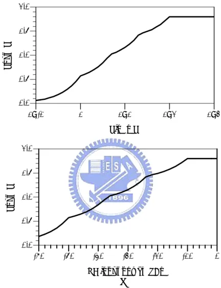
Here, we give a simple example of logarithmic amplifier that convert 70 dB dynamic range from -60 to10dBm (0.1mV~1000mV) input into a 0~1.8V output with four stages of limiting amplifier. Since four stages are used, then and
choose . The first transition point is at -50dBm, and means
that 4VL≤ 81. 0.45 L V = 4 1 L v V mV
A = andAV =4.605. Fig. 2-7 is the simulation done by behavior model in 14
ADS environment.
The logarithmic function is useful but at the cost of hardware and design complexities. The following two chapters are some RF power detection designs that use comparing methods instead of trying to obtain the absolute power levels.
1 1E1 1E2 1E-1 1E3 0.5 1.0 1.5 0.0 2.0 Vin (mV) V out ( V ) -50 -40 -30 -20 -10 -60 0 0.5 1.0 1.5 0.0 2.0 RF input power (dBm) Vo u t (V) (a) (b)
Fig. 2-7 Behavior model simulation of a log amp (a) Vout vs. Vin in log-scale (b) Vout vs. corresponding of Vin to 50Ohm
Chapter III
RF power detection circuit design in WiMAX
transmitter
3.1
Motivation
The standard of IEEE 802.16 family, popularly known as WiMAX, provides wireless transmissions of high data rates over metropolitan areas. The transmitted signal format may include complicated modulation such as 64-QAM. To ensure correct data receiving, the measure of EVM (error vector magnitude) quantifies the error of transmitted signals and defines the performance of digital radio transmitters. It is therefore critical to minimize the EVM. Many non-ideal circuit effects contribute to EVM degradation in the RF end, including LO phase noise, carrier feed-through, I/Q imbalance, and nonlinearity. The normal figure of transmitter circuitry achieves the level from -20dB to -25dB. In the latest released WiMAX mobile standard, however, it defines a severe EVM level of -30dB which implies more advanced circuit designs is necessary.
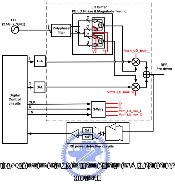
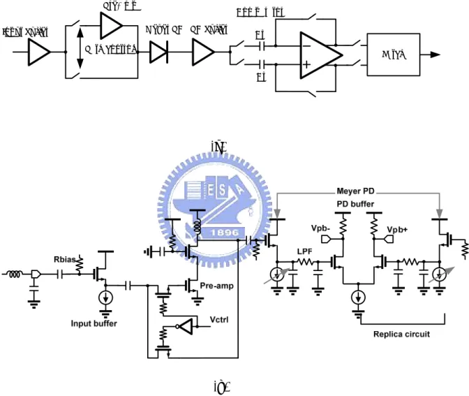
Fig. 3-1 is the architecture of the proposed direct up-conversion mixer with auto-calibration for I/Q imbalance and LO feedthrough. The IF and RF frequency is designed at 10MHz and 2.6GHz respectively. The dotted box is the open loop design done by me senior [1]. It consists of two LO buffers to tune the gain/phase mismatch errors and IDACs on the transconductance stage of the Gilbert cell mixers to suppress the LO feedthrough. All of them are digitally controlled by the 3-wire shift register.
In order to accomplish an auto-calibrated closed loop system, a RF power 16
detection circuitry that consists of a pre-amplifier, a power detector, sample and hold circuit (S/H), and a comparator is necessary. This RF to digital interface first samples the RF power of a bit and holds the converted DC output of the PD. After that, we tune the next control bit, this signal is also converted to DC by the PD. The comparator distinguishes which one if larger and gives logic output to the digital circuits to tune the bit higher or lower.
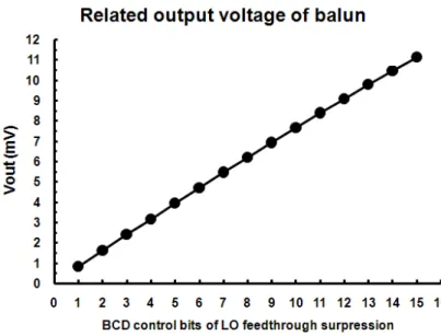
In LO feedthrough compensation mode, baseband signals are not fed to the mixers so that LO feedthrough signals can be directly detected at the RF output of the mixers. Fig. 3-2(a) plots the simulation results of LO feedthrough of one side of the differential output. An external balun is used to combine the differential output of I/Q mixer since the power detection circuit is single-ended input. Fig. 3-2(b) is the calculation of equivalent output voltage of the balun to 50 Ohm.
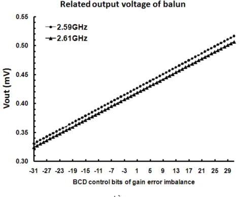
In gain imbalance compensation mode, we use baseband test vectors (A,0) and (0,A). The gain imbalance can be suppressed which means the ratio of the output power is minimized by tuning the LO Q buffer. In phase calibration mode, we use baseband vectors (A,A) and (A,-A) and the phase mismatch is minimized by tuning the I buffer. According to my senior’s simulation and calculations, the levels of RF output signals during gain and phase calibration are the same. However, the bit difference of gain error is smaller which means phase error can be detected so long as gain error is detected. Fig. 3-3(a) plots the simulation results of gain error and Fig. 3-3(b) is the equivalent output voltage of the balun to 50 Ohm.
θ
V
θ
V
Fig .3-1 Direct up-conversion mixer with auto-calibration for I/Q imbalance and LO feedthrough
(a)
(b)
Fig. 3-2 (a) LO feedthrough of one side of the I/Q mixer’s output vs. control bits (b) Related output voltage after balun vs. control bits
(a)
(b)
Fig. 3-3 (a) The RF output signal of I/Q mixer’s during gain error test vs. control bits (b) Related output voltage after balun vs. control bits
3.2
RF power detection circuit design
From the previous section, we can know that detection circuit must be capable to detect wide dynamic and small differences RF signals, such as LO feedthrough from 0.84mV to 11.14mV with minimum bit difference of 0.66mV and gain error signal from 321mV to 516mV with minimum bit difference of 2.9mV.
Fig. 3-4(a) and (b) are the architecture and schematic of the RF detection block. In order to have lower losses, a source follower (SF) is employed as an input buffer at the front-end of the detection path. Since only the linear region of a Meyer PD can produces a comparable input for the comparator, small LO signals need to be amplified first. Therefore, the detection path is divided into two: an amplification path for the LO leakage and a bypassing path or the gain/phase error. A simple control switch is used o choose which path is turned on. The Meyer PD then converts the
detected RF signals to a DC level. However, not only the DC output levels but also their differences are too low for the comparator to compare. An additional PD buffer is necessary to amplify the DC signals once again. Besides, it also supports a good isolation between the Meyer PD and the comparator. The following are some descriptions for each circuit building block.
Latch Input buffer Pre-amp Path control Meyer PD PD buffer Cs Cs Comparator (a) (b)
Fig. 3-4 (a) RF power detection architecture (b) Schematic of the RF power detection circuits before the comparator
3.2.1 Input
buffer
As depicted in Fig. 3-4(b), the source follower is designed to match 50 Ohm taking the parasitic effects of pad and bond wire into account. Hence, measurements
can be made with open loop design or alone. If the size of Rbias it too large, the source
follower output impedance contains an inductive component. The dependence of this inductive component upon Rbias implies that if a source follower is driven by a large
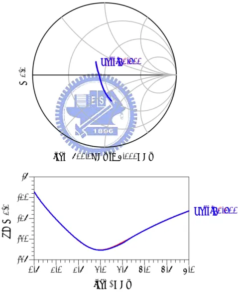
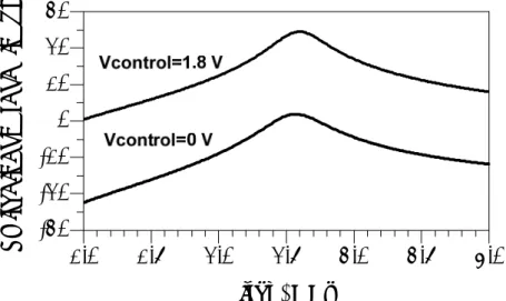
resistance, then it exhibits substantial inductive behavior [22]. Here, a small size of 50Ohm is used both for preventing this effect and matching to the input 50Ohm port. Fig. 3-5 is the simulation result of the input impedance of the RF detection circuit. It shows that a smaller than -20dB of input return loss is sufficient.
Vctrl=0.000 Vctrl=1.800 freq (500.0MHz to 4.000GHz) S( 1 ,1) 1.0 1.5 2.0 2.5 3.0 3.5 0.5 4.0 -20 -15 -10 -25 -5 Vctrl=0.000 Vctrl=1.800 freq, GHz d B (S (1 ,1 ))
Fig. 3-5 Simulation of input matching
3.2.2 Pre-amplifier
The pre-amplifier uses a simple cascode topology with inductive shunt peaking
to amplify the LO feedthrough signals with 25dB at 2.59~2.61GHz. Fig. 3-6 is the simulation results of the switching path in amplification mode and bypass mode.
1.5 2.0 2.5 3.0 3.5 1.0 4.0 -20 -10 0 10 20 -30 30 freq, GHz S w it ch in g_ pa th_ g ai n (dB )
Fig. 3-6 Simulation of the switching path
3.2.3
Meyer power detector & PD buffer
As discussed in the previous chapter, there are two regions in the transfer curve of the Meyer PD: square law and linear. If the square law region is used, the output voltage is too small to compare. So it is necessary to add a stage of log amp. In order to reduce the circuit complexities and to save power, we use the linear region instead.
The schematic of the Meyer PD is the same as Fig. 2-2. In order to make the M1 and M2’s sub-threshold current sources Ib1 and Ib2 work at their saturation region
properly, the dimensions of M1 and M2 are chosen as large as 5um*50/0.18um. As
depicted in Fig. 3-7(a), the transfer curve of a Meyer PD is plotted a little bit different from Fig. 2-2, which x-axis and y-axis are changed to linear voltage, so as to make observations of linear region easier. Fig. 3-7(b) shows the slope of Fig. 3-7(a). As can be seen, the slope of the Meyer PD is below unity. It implies that the output difference of each bit is below the comparable difference. Notice that the comparator’s threshold
voltage is assumed conservatively 1.3mV.
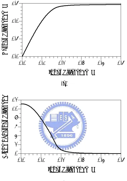
A PD buffer, which is a simple differential-pair, is added to solve this problem. As shown in Fig. 3-8(a) the differential pair is designed to have a wide linear input range. Fig. 3-8(b) plots the slope of Fig. 3-8(a) to check how much the bit difference can be amplified. In practical implementations, DC offsets is unpreventable both on the Meyer PD and PD buffer. As indicated in Fig. 3-4(b), the DC offset is compensated by tuning the current sources of the Meyer PD and observing the DC output voltage of the PD buffer. Fig. 3-9 is the combination simulation results of the circuits before the comparator. Fig. 3-9(a) is a 0.84mV, 2.59GHz input signal and changes 0.66mV larger after 2usec. Fig. 3-9(b) shows that the DC output difference of the PD buffer changes 3mV larger.
0.2 0.4 0.6 0.8 1.0 1.2 1.4 1.6 0.0 1.8 0.2 0.4 0.6 0.8 1.0 0.0 1.2 Input voltage (V) O u tp u t vo lt ag e (V ) (a) 0.2 0.4 0.6 0.8 1.0 1.2 1.4 1.6 0.0 1.8 -0.0 0.2 0.4 0.6 0.8 -0.2 1.0 Input voltage (V) O u tp u t vo lt ag e sl o p e 24
(b)
Fig. 3-7 (a) Meyer PD transfer curve (b) slope of the transfer curve
0.1 0.2 0.3 0.4 0.0 0.5 0.5 1.0 0.0 1.5 Input difference (V) Outp ut di ffe re n ce (V ) (a) 0.1 0.2 0.3 0.4 0.0 0.5 2 4 6 8 10 0 12 Input difference (V) S lope of out put dif fe re nc e (b)
Fig. 3-8 (a) PD buffer transfer curve (b) slope of the transfer curve
1.
998
1.
999
2.
000
2.
001
2.
002
2.
003
1.
997
2.
004
-1
0
1
-2
2
time, usec
T
R
AN.
V
in
, mV
(a) 0.5 1.0 1.5 2.0 2.5 3.0 3.5 0.0 4.0 0.000 0.001 0.002 0.003 -0.001 0.004 time, usec V out (b)Fig. 3-9 Simulation results of the circuits before comparator
3.2.4 Comparator
Fig. 3-10 Schematic of comparator (a) Pre-amplifier (b) Latch
Fig. 3-10 is the schematic of the comparator employed in the power detection circuitry. This topology merges S/H and comparator together. In order to prevent kickback noise, the comparator is separated into pre-amp and latch. The differential mode gain of the cross couple load of the pre-amp can be expressed as (3.1). The common mode gain can be expressed as (3.2).
1,2 5,6 3,4 1 DM m m m A G G G = − (3.1) 27
1,2 1,2 3,4 5,6 1 1 2 m CM m O m m G A G r G G = + + (3.2) CLK CLK1 CLK1d
Fig. 3-11 Timing of the comparator
In order to compare the RF power of two control bits, the timing is set as Fig. 3-11.
1. CLK1=”1”, CLK1d=”1”, CLK=”0”:
The PD converts the RF output power of the first bit to DC The pre-amplifier acts as a unit gain buffer. Both DC offset and the converted DC output of the first bit, Vtime1 is hold in the sampling capacitor, Cs while latch is in the reset mode and
outputs “logic 1”.
2. CLK1=”0”, CLK1d=”1”, CLK=”0”:
After switching to next compensation bit in the open loop circuits, the PD converts RF output power to a DC voltage, Vtime2. The pre-amplifier then
compares Vtime1 and Vtime2. DC offset is cancelled. The latch still remains in the
reset mode.
3. CLK1=”1”, CLK1d=”1”, CLK=”1”:
The amplified difference of Vtime1 and Vtime2 is past to the latch. The latch pulls it
to logic high or low. Fig. 3-12 is the simulation result of the comparator.
0.002 0.003 0.001 0.004 Vi n (V ) 0.5 1.0 1.5 0.0 2.0 CL K1 ( V ) 0.5 1.0 1.5 0.0 2.0 CL K1d ( V ) 0.5 1.0 1.5 0.0 2.0 CL K ( V ) 0.5 1.0 1.5 2.0 2.5 3.0 3.5 4.0 4.5 0.0 5.0 0.0 0.5 1.0 1.5 -0.5 2.0 Time (msec) V out ( V ) (a) 29
0.002 0.003 0.001 0.004 Vi n (V ) 0.5 1.0 1.5 0.0 2.0 CL K1 ( V ) 0.5 1.0 1.5 0.0 2.0 CL K1d ( V ) 0.5 1.0 1.5 0.0 2.0 CL K ( V ) 0.5 1.0 1.5 2.0 2.5 3.0 3.5 4.0 4.5 0.0 5.0 1.0 1.5 0.5 2.0 Time (msec) V out ( V ) (b)
Fig. 3-12 Simulation results of the comparator
3.3
Simulation results
The simulation results of LO feedthrough compensating modes and gain error compensating mode is shown in Fig. 3-13.
-30 -20 -10 0 10 20 30 -40 40 1.1 1.2 1.3 1.4 1.0 1.5
gain error control bit change
D et e ct ion bl oc k ou tput ( V ) 0. 00 1 0. 00 2 0. 00 3 0. 00 4 0. 00 5 0. 00 6 0. 00 7 0. 00 8 0. 00 9 0. 01 0 0. 00 0 0. 01 1 0.05 0.10 0.15 0.00 0.20
LO leakage output voltage (V)
D et ec ti on bl oc k out put ( V )
Fig. 3-13 Simulation results of (a) gain error (b) LO feedthrough
3.4
Chip layout & summary
Fig. 3-14 Layout of the RF power detection circuit
Fig. 3-14 is the chip layout in TSMC 0.18m technology. The chip size is mainly limited by the number o pads. Therefore, using large area of RF P-cells for the comparator doesn’t matters. The layout area is 1.055X0.9 mm2.
Unfortunately, the 3-wire control of open loop chip is latched-up and no functional verifications for practical implementations can be made. Hence, the power detection design that is to meet the specifications of that chip has not been fabricated yet. In the future, identifications of the chip failure and re-consider some of the design issues will be made first. After that, we will integrate both designs and complete an auto-calibrated I/Q modulator.
Chapter IV
Built-in self-test circuit designs for 5GHz LNA
4.1
Introduction
With the mature progress in CMOS technology nowadays, integrating more and more functional analog and digital building blocks into a single chip solution is a trend. However, this increases not only the cost but also the complexities of test. Embedded built-in self-test (BIST) on chip seems to be a good solution. In contrast to digital and analog circuits that BIST has been widely utilized, RF BIST circuit designs are still in the early-age development.
The recent proposed BIST architectures can be categorized into loop back test for overall RF transceiver [8] and individual circuit block tests with the aid of embedded power detectors (or RMS detectors) [6]-[10]. The latter testing methods depend on the accuracy of power detector (PD) to measure the absolute input and output power level of the circuit under test (CUT). As such, a logarithmic amplifier (Log amp) is necessary to convert the output level from dB-linear into linear scale [10].
In this chapter we proposed a power comparing method to monitor the status of the CUT. This technique alleviates the loading of the PDs and shifts the accuracy difficulties to a digital step attenuator (DSA). Meanwhile, a low dynamic range PD is sufficient. By using a 3-bit digital control, the goal of monitoring our CUT, a 5GHz low noise amplifier (LNA) can be achieved. Moreover, an invention of the R-72R that deals with the process variations of the most critical block of the BIST circuitry, the DSA, is also introduced in this chapter.
Section 4.2 gives detailed descriptions of RF BIST design with a digital step attenuator. Both simulation results and experimental are also shown in this section. In Section 4.3, a new configuration of R-72R ladder gives a solution to the process variation issue in Section 4.2. Last, a conclusion and summary is given in Section 4.4.
4.2
RF BIST design with a digital step attenuator
4.2.1
The BIST architecture
Fig. 4-1 Proposed BIST architecture
Fig. 4-1 is the proposed BIST architecture including a 15.XXdB 5GHz LNA as our CUT and the BIST module. Two PDs are employed to convert RF signals into DC levels. The switch at the left hand side (SWA) contributes -2dB attenuation. The switch
at the right hand side (SWB) along with a 3 bit 8 level DSA contributes a tunable
attenuation from -8dB to -15dB. The overall attenuation of the detection circuit is
B
therefore -10dB~-17dB. The comparator in the bottom compares the DC levels of Vpd1 and Vpd2. In this work, the comparator has not been integrated in yet. Instead, a
DC voltage meter will be used in the measurement to verify the idea.
Fig. 4-2 (a) Operating mode (b) Test mode
As shown in Fig. 4-2, the BIST circuit can be switched between two modes: (a) Operating mode:
As shown in Fig. 4-2(a), we turn off SWA and SWB in order to make the LNA
operates normally. The RF signal delivers from RF
B
in to RFout. We can use network
analyzer and signal generator along with spectrum analyzer to do the LNA measurement as what we always do.
(b) Test mode:
As shown in Fig. 4-2(b), we turn on SWA and SWB to connect our CUT with the
BIST module and move our input from RF
B
in to RFtest. The test RF signals will be
generate from the local oscillator (LO) when this architecture is integrated into a transceiver in the future. For verifying the idea, signal generator will be used instead. The test signals will be swept around 5GHz since we cannot know exactly whether the CUT is still peaking at 5GHz or not due to the process variations and all kinds of
design uncertainties. The test power level cannot be too high a level due to the linearity of the CUT and cannot be set too low that will generate a too low DC level from the PD. Thus, I fixed it at an appropriate value of -25dBm.
As indicated in Fig. 4-2(b), there are two paths for the 5GHz test signal. It travels downwards to let PD1 convert it into a DC level Vpd1. It travels upwards through SWA, CUT (LNA), SWB, DSA, and finally PD2 convert it to another DC level Vpd2.
We can tune the 3 control bits of the DSA with 1dB/step.
B
Initially, we start from the control bit 000 which is a lowest attenuation level and Vpd2 will be greater than Vpd1. The comparator will give us a “logic 1” output. By
tuning controls bits, the attenuation level increases 1dB higher per bit that eventually makes Vpd2 larger than Vpd1. The comparator output will then switch from “logic 1” to “logic 0”. At this certain bit, the gain of the CUT can be known by us. In this work, the CUT is designed with the gain of 15~16dB in the TT corner. From Table.1below, we can know that when we switch from 101 to 110, Vpd (=Vpd2-Vpd1) will switch from positive to negative ideally.
Table 1 Attenuation levels
Control bit Attenuation
(dB) 0 000 -10 1 001 -11 2 010 -12 3 011 -13 4 100 -14 5 101 -15 6 110 -16 7 111 -17
In this version the comparator is not integrated in the BIST module yet.
Neglecting the threshold voltage of the comparator, we postulate that Vpd=Vpd2-Vpd1>0, gives “logic 1” and Vpd=Vpd2-Vpd1≦0, gives “logic 0” for simplicity. The following sections are the circuit building blocks in Fig. 4-1.
4.2.2
Low noise amplifier
M2 RFin LS Cex M1 Lg Ld RFout Cd Vg_LNA Vbuffer M3 M4
Fig. 4-3 Circuit under test: a 5GHz low noise amplifier
Fig. 4-3 is the CUT that uses a conventional cascode LNA topology [21]. Ls, Lg, and Cex give us the simultaneous input impedance and noise matching. The transistor M2 is adopted for excellent reverse isolation and the output LC-tank composed of Ld
and Cd make the S21 peak at 5GHz. For measurement considerations, a source
follower, consists of M3 and M4, is added to match the output port to 50 Ohm.
4.2.3 Switch A (SW
A)
Fig. 4-4 Switch A
Depicted in Fig. 4-4, an πattenuator that has -2dB attenuation is adopted for SWA for the sake of matching the CUT with the test port. The linearity issue of the
attenuator can be ignored since the test signal is as low as -25dBm. Therefore, resistors of an π attenuator can all be replaced by MOSFETs as switches. A large HRI resistor of several Kilo-Ohms is connected from the bulk of M1 to ground for the purpose of minimizing the parasitic effects. Furthermore, two large resistors RB are
connected to from source and drain to ground to prevent DC level uncertainties.
B
4.2.4
Power detector (PD)
Fig. 4-5 (a) Threshold voltage of the comparator (b) PD characteristic curve
In this BIST architecture, the power detectors are not only to convert RF signals into DC voltages but also need generate a comparable voltage difference for the comparator. In Fig. 4-5(a), we can define the threshold voltage of the comparator as Vx. The comparator outputs a “logic 0” if the input is below it. For the following
analysis, we simply model the transfer function of a power detector as:
2
pd in
V =KV
(4.1) where K is a constant representing the PD characteristic.
The input of the comparator which is the output difference of the PDs can be expressed as: 21 2 1 2 2 2 2 2 2 10 - ( 1) (10 att 1) pd pd pd 2
LNA att test test
test S S test V V V KA A V KV KV A KV + = − = = − = − (4.2)
where ALNA is the voltage gain of the LNA, AATT is the voltage attenuation of the
attenuator, and Vtest is the test voltage. We also assume perfect matching to 50Ohm
between inter stages. The design parameters will then be simplified to K and Vtest by
(4.2). We can know that the larger the K the more relaxed for the comparator. Employing the Meyer PD in Section 2.2 is the first thought came to mind. However, the following analysis tells us that Meyer PD has its own limitations in this application.
Fig. 4-6 (a) Meyer power detector (b) Current amplifier power detector
A bit different from Fig. 2-1, the Meyer PD in Fig. 4-6(a) has input signals on both transistors, M1 and M2.
Using the results of (2.3), the DC current of M1 can be re-written as:
2 4 2 4 1 1 0 2 2 1 0 3 1 1 1 1 exp[ ]*[1 ( ) ( ) ...] 2! 2 4! 8 1 1 exp[ ]*[1 ( ) ] 2! 2 GS THN test test D D T T T GS THN test D T T V V V V W I I L nV nV nV V V V W I L nV nV − = + + − ≈ + + (4.3) Similarly, 2 2 2 2 0 1 1 exp[ ]*[1 ( ) ] 2! 2 GS THN att D D T T V V V W I I L nV nV − ≈ + (4.4) Since identical current sources are used:
1 2 2 2 2 2 1 2 0 0 2 2 1 2 2 2 2 2 1 2 1 1 1 1 exp[ ]*[1 ( ) ] exp[ ]*[1 ( ) ] 2! 2 2! 2 1 1 [1 ( ) ] 2! 2 exp[ ] 1 1 [1 ( ) ] 2! 2 1 1 *[ln(1 ( ) ) ln(1 2! 2 D D GS THN test GS THN att D D T T T T att GS GS T T test T att GS GS T T I I V V V V V V W W I I L nV nV L nV nV V V V nV nV V nV V V V nV nV = − − ⇒ + = + + − ⇒ = + ⇒ − = + − + 1 ( 1 )2 2)] 2! 2 test T V nV (4.5) By means of the Maclaurin Series below,
2 3 4 1 ln(1 ) ... ( 1) ... (-1< 1) 2 3 4 1 n n x x x x x x x n + + = − + − + + − + ≤ + (4.6) (4.5) can be approximated as:
2 1 2 1 ( 4 GS GS att test T V V V V nV − = − 2) (4.7) So finally, with (4.7) Vpdcan be expressed as:
2 2 1 2 1 1 2 1 ( ) ( ) ( 4 2) pd pd pd b GS b GS GS GS att test T V V V V V V V V V V V nV = − = − − − = − = − (4.8)
We can know from (4.7) that 1
4 T
K nV
= and this value is too low.
Depicted in Fig. 4-6(b), the topology of current amplifier PD [3] is adopted to overcome the design difficulties due to small K of Meyer PD. The concept of nonlinearities of a transistor is much similar to Meyer PD if we bias M1 at its sub-threshold region. M2 and M3 compose a current mirror and amplify the sub-threshold current generated from M1 by their ratio. RL then converts this current
into voltage. Last, two stages of low pass filter are added to filter out the high
frequencies and just to keep their DC levels.
We can express the descriptions above all in one equation:
2 3 1 0 1 2 2 2 ( / ) ( / ) *exp( )*(1 ) ( / ) 4 GS m pd D L T W L V V V I W L R W L nV n V = + T (4.9) Therefore, the difference of the PDs’ output can be derived as follow:
2 3 1 0 1 2 2 2 2 3 2 0 1 2 2 2 2 2 3 2 1 0 1 2 2 2 ( / ) ( / ) * exp( ) * (1 ) ( / ) 4 ( / ) ( / ) * exp( ) * (1 ) ( / ) 4 ( / ) 1 ( / ) * exp( ) ( ( / ) 4 GS RFtest pd D L T T GS DSAout pd D L T T GS pd pd pd D L DSAout in T T W L V V V I W L R W L nV n V W L V V V I W L R W L nV n V W L V V V V I W L R V V W L nV n V = + = + = − = − ) (4.10) Obviously, the K for current amp PD can be designed suitable in this application.
Notice that the path in test mode is designed in power domain which is a 50Ohm-environment in order to make the detected voltage closed to the power gain (S21). The bias resistor, Rbias, of PD2 is set to a value near 50Ohm. Since SWA is
already has input impedance matched to 50Ohm, we only need a large Rbias for PD1 to
minimize the loading effects.
Fig. 4-7 is the simulation results of a current amp PD designed in TSMC 0.18um technology. We can see from Fig. 4-7(a) that the output of the PD rises from its initial DC bias point (517.5mV) when there is a RF signal input. The output reaches its steady state around 25ns. Fig. 4-7(b) is result of the harmonic balance simulation. The input power is swept from -30dBm to 10dBm. The simulation results show that the output difference of -25dBm and -24dBm input is around 3mV which is sufficient for the comparator.
5 10 15 20 25 0 30 520 540 560 580 600 620 640 500 660 time (nsec) P D ou tp ut (V ) (a) -25 -20 -15 -10 -5 0 5 -30 10 0.6 0.8 1.0 1.2 1.4 1.6 0.4 1.8
RF input power (dBm to 50Ohm)
P D D C oup ut v ol ta ge (b)
Fig. 4-7 (a) Time response with different input levels (b) DC output voltage vs. input power
4.2.5
Digital step attenuator (DSA)
Fig. 4-8 (a) shows the configuration of the DSA. By switching between the two attenuation levels of the attenuation cell a -8~-15dB with -1dB/step can be achieved. Fig. 4-8 (b) is the attenuation cell used. Here I called it a “complementary
π
attenuator”. Matching closed to 50 Ohm while switching betweenthe two attenuation levels is a merit. Besides this, the signal at the output of the LNA is larger and causes linearity to be an issue. Resistive network, however, has high linearity that will be suitable here. Here, inverter is used to give us D1 and D1b. For larger attenuation levels, we can turn on D1 and turn off D1b to make the series resistance larger and shunt resistance smaller and vice versa for smaller attenuation levels.
Fig. 4-8 (a) Digital step attenuator (b) attenuation cell
In order to make the power gain equal to the voltage gain, the DSA is designed to make the input impedances closed to 50Ohm (or S11<-20dB). Besides, a very linear 1dB-attenuation is necessary simultaneously at each step. Besides the lowest attenuation level -7dB of the DSA itself, an additional 1dB loss is contributed from
SW2 and the AC couple capacitor between the DSA output and the gate of PD’s M1 to make the lowest attenuation of this path -8dB.
Fig. 4-9 are some simulation results of Fig. 4-8 (a) using a -10dBm which has 50Ohm source resistance 5GHz input test tone. Fig. 4-9(a) shows the power level at Vg2 referring to 50Ohm. If we view the DSA as a DAC, the bit difference or DNL can
be simply define as:
( ) ( 1)
( ) (LSB)
1
output power i output power i Bit difference i
dB
− −
=
(4.11) where LSB equals to 1dB. Fig. 4-9(b) is a plot of bit difference after calculations. Fig. 4-9(c) plots the variations of input impedance.
(a)
(b)
(c)
Fig. 4-9 (a) Output power of the DSA with -10dBm test tone (b) Bit difference (c) Input impedance check
4.2.6
Design guidelines of the DSA
One may wonder how the DSA is designed so perfectly as the Fig. 4-9. No doubt a beginner may spend hours and hours, days and days on trimming owing to the non-idealities of the component values, such as parasitic effects and turn on/off resistance of the MOS. Here, we came up to some design guidelines not great as a theory but just to let us never become an “ADS tuning monkey!” The following steps are the designer’s “know how.” Belief it or not, rapid and efficient design can be made by following them.
Step I: One can first calculate the ideal values of Rs, Rsb, Rp, and Rpb in Fig. 4-8(b). Construct an ideal attenuation cell with the calculated resistor values, an ideal switch, and an inverter. Double check the attenuation levels (or S21)
of the two modes and the input impedance Zin. Make sure that one designs
one attenuation cell at a time. Please don’t haste to combine the attenuation cells altogether at the very beginning or you might in big trouble.
Step II: Change the ideal series switch to Ms and sweep the dimension of it. Take a glance at both S21 and Zin. One can notice that larger dimensions of Ms
result in a more ideal S21. However, this causes the real part of Zin to shrink
more than smaller dimensions. One may stupidly want to make the Rsb smaller, since it is series with an on resistance of Ms. However, the results are even worse. The smaller the Rsb, the more Zin shrinks
Step III: Sweep the size of Rp instead. One may notice that by making the size few tens Ohms larger than the calculated value, the results will be closer to the ideal value. Besides, Zin doesn’t shrink anymore. We can conclude shortly
that the series branch of an attenuation cell is the most sensitive part. Don’t ever try to change it.
Step IV: Change the ideal parallel switch to Mp. Larger dimension size results in a smaller on resistance and a bigger off capacitance that makes “000” the smallest Zin when combing the attenuation cells together. As Rs, Rsb, and
Rp are fixed already from Steps I~III, Rpb is the only degree of freedom left.
Chance of fixing the attenuation cell closer to ideal is to make Mp smaller and Rpb bigger.
Step V: Since the estimated values is given from steps above, change the resistors to practical ones, such as HRI, RP-poly, etc. A little bit of fine tuning the component size afterwards is necessary since there are still some parasitic effects of the practical resistors.
Step VI: Finally, do the same steps to design each attenuation cell and combine them together.
A point to mention is that attenuation cells are easier to design if the difference of the two desired attenuation levels is not so high since Zin won’t be switched so
severely.
4.2.7 Post-simulation
results
Fig. 4-10 is the results of the operating mode using Cadence Spectre RF and Ansoft Designer for post layout EM simulation. I organized these data in Table 2 that can give us the reference information for the test mode.
(a) Operating mode
SS
TT
FF
(b)
Fig. 4-10 Post simulation results of the CUT (a) S11 &S21 (b) Noise figure (c) S11
Smith Chart (d) S22 Smith Chart
Table 2 Performance summary of the CUT in operating mode
Corner case TT SS FF S21 peak 15.68 dB @5GHz 12.81 dB @4.60GHz 18.35 dB @5.45GHz S11 dip -30.88 dB @5GHz -21.72dB @4.67GHz -31.49dB @5.419dB S22 dip -22.20 dB @5GHz -19.45dB @4.58GHz -26.81dB@5.51dB Noise figure 2.867 dB @5GHz 3.33dB @4.67GHz 2.541dB @5.42dB (b) Test mode
According to Table 1&2, the zero crossing point of Vpd (Vpd2-Vpd1) should occurs
at 101 to 110 for TT corner case, 010 to 011 for SS ideally. Since the gain of the FF corner is out of range, we just consider the quantity is larger than 17dB. The simulation result is plotted in Fig. 4-11. Since the BIST module is designed in TT corner case, its function is correct. However, the zero crossing occurs at 011 to 100 or SS corner which is a bit next to the ideal. This is somewhat tricky. In order to obtain a correct BIST function, an invariable circuit is to test a variable circuit (CUT). However, we forgot that that the BIST circuitry also varies with process and temperature variations during design. This issue will be discussed further in Section 4.3.
Fig. 4-11 Test mode: The output difference of the two power detectors vs. control bit