國
立
交
通
大
學
電子工程學系 電子研究所
博 士 論 文
矽奈米尺寸金氧半場效電晶體的載子傳輸與
矽奈米尺寸金氧半場效電晶體的載子傳輸與
矽奈米尺寸金氧半場效電晶體的載子傳輸與
矽奈米尺寸金氧半場效電晶體的載子傳輸與
重要元件參數之
重要元件參數之
重要元件參數之
重要元件參數之實驗性
實驗性
實驗性的
實驗性
的
的
的研究
研究
研究
研究
Experimental Study of Carrier Transport and Important
Device Parameters for Nanoscale Si MOSFETs
研 究 生:李維
指導教授:蘇彬 教授
中
中
中
矽奈米尺寸金氧半場效電晶體的載子傳輸與
矽奈米尺寸金氧半場效電晶體的載子傳輸與
矽奈米尺寸金氧半場效電晶體的載子傳輸與
矽奈米尺寸金氧半場效電晶體的載子傳輸與
重要元件參數之實驗性的研究
重要元件參數之實驗性的研究
重要元件參數之實驗性的研究
重要元件參數之實驗性的研究
Experimental Study of Carrier Transport and Important
Device Parameters for Nanoscale Si MOSFETs
研 究 生:李維 Student:Wei Lee
指導教授:蘇彬 博士 Advisor:Dr. Pin Su
國 立 交 通 大 學
電子工程學系 電子研究所
博 士 論 文
A DissertationSubmitted to Department of Electronics Engineering and Institute of Electronics
College of Electrical and Computer Engineering National Chiao Tung University
in partial Fulfillment of the Requirements for the Degree of
Doctor of Philosophy in
Electronics Engineering
February 2009
矽奈米尺寸金氧半場效電晶體的載子傳輸與
矽奈米尺寸金氧半場效電晶體的載子傳輸與
矽奈米尺寸金氧半場效電晶體的載子傳輸與
矽奈米尺寸金氧半場效電晶體的載子傳輸與
重要元件參數之實驗性的研究
重要元件參數之實驗性的研究
重要元件參數之實驗性的研究
重要元件參數之實驗性的研究
研 究 生:李維 指導教授:蘇彬 博士
國立交通大學 電子工程學系 電子研究所
摘要
本論文針對多閘極金氧半場效電晶體,比較其載子傳輸在重疊與非重疊閘 源(汲)極結構中之差異,在具有重疊結構的元件中,我們觀察到次臨界電流特 性依循波玆曼定律以及聲子為主要之載子碰撞特性,而在非具有重疊閘源(汲) 極結構的元件中,我們發現次臨界區域與反轉區域之汲極電流對溫度並不敏感。 我們的低溫量測結果指出,對於窄的重疊結構元件而言,載子在能階間碰撞是傳 輸的主要機制,而對於非重疊結構元件而言,存在於非重疊區域的位能障會導致 電導降低以及擾動。 此外,我們針對非具有重疊閘源(汲)極結構的多閘極金氧半場效電晶體, 有系統地分析其可被控制的單電子效應與通道長、通道寬、閘極電壓、溫度之間 的相依性。我們的研究指出,使用非重疊閘源(汲)極結構有助於實現單電子電 晶體於金氧半場效電晶體,同時多閘極結構提供高閘極控制能力與高源(汲)極 電阻的雙重優點,單電子效應被進一步地強化,目前的結果顯示,如果要實現室 溫下可運作的單電子電晶體,除了元件尺寸必須要進一步維縮之外,穿隧位能障 以及源(汲)極電阻必須要再進一步最佳化。由於單電子效應可被實現於最先進以達到高密度的目的。 另外,我們評估從實驗中萃取通道背向散射的可行性、限制因素以及應用 範圍,我們的研究指出,其困難點在於是否能正確決定低電場載子遷移率(µ0)、 關鍵長度(l)與熱速度(υtherm)的溫度係數,透過我們所提出的自我相符萃取方 法,我們不必預先假設:平均自由徑 λ = (2kBTµ0/qυtherm),l = kBT 長,µ0 =低電場載 子遷移率,以及非退化極限。用這個廣義溫度相依性的萃取方法來分析應力效應 對通道背向散射的影響,我發現 p 型金氧半場效電晶體之通道背向散射會因單軸 壓縮應力增強而下降。至於應力效應與靜電位能的相關性,第一次透過實驗方法 萃取出。我們還進一步證實應力作用能夠透過增強彈道傳輸效率進而抑制汲極電 流的變異。 還有,我們針對具有超薄氧化層的金氧半場效電晶體,研究其漏電流所引 起異常電容電壓特性的問題,我們提出用本質輸入阻抗來模擬長通道金氧半場效 電晶體之電容衰減,並反向重建應有的電容電壓特性,透過 SPICE (Simulation Program with Integrated Circuit Emphasis)模擬,我們驗證本質輸入阻抗重建衰減電 容的可靠度,而對於所重建的電容電壓特性,我們發現多晶矽閘極空乏效應可以 被真實呈現,這個突破是有別於傳統使用頻率相依性所重建出的結果。由於重建 方法的簡單性,因此適合作為大量製程觀察之用。 關鍵字 關鍵字 關鍵字 關鍵字:金氧半場效電晶體、量子干涉、單電子、彈道傳輸、背向散射、電容
Experimental Study of Carrier Transport and Important
Device Parameters for Nanoscale Si MOSFETs
Student:Wei Lee Advisor:Dr. Pin Su
Department of Electronics Engineering and
Institute of Electronics
National Chiao Tung University
Abstract
This thesis provides a comparative study of carrier transport characteristics for multiple-gate silicon-on-insulator (SOI) metal-oxide-semiconductor field-effect transistors (MOSFETs) with and without the non-overlapped gate to source/drain structure. For the overlapped devices, we observed the Boltzmann law in subthreshold characteristics and phonon-limited behavior in the inversion regime. For the non-overlapped devices, however, we found insensitive temperature dependence for drain current in both subthreshold and inversion regimes. Our low-temperature measurements indicate that the inter-subband scattering may be the dominant carrier transport mechanism for narrow overlapped multiple-gate SOI MOSFETs (MuGFETs). For the non-overlapped MuGFETs, the voltage-controlled potential barriers in the non-overlapped regions are crucial and may give rise to the conductance reduction and fluctuation.
Besides, we systematically present controlled single-electron effects in the non-overlapped MuGFETs with various gate length, fin width, gate bias and temperature. Our study indicates that using the non-overlapped gate to source/drain
structure as an approach of the single-electron transistor (SET) in MOSFETs is promising. Combining the advantage of gate control and the constriction of high source/drain resistances, single-electron effects are further enhanced using the multiple-gate architecture. From the presented results, downsizing MuGFETs is needed for future room-temperature SET applications. Besides, the tunnel barriers and access resistances may need to be further optimized. Since single-electron effects can be achieved in state-of-the-art MOSFETs, it is beneficial to build SETs in low-power complementary metal-oxide-semiconductor (CMOS) circuits for the ultrahigh-density purpose.
In addition, we have assessed the validity, limitation, and application of experimental channel backscattering extraction. Our study indicates that the difficulty of the temperature-dependent method lies in accurate determination of the temperature sensitivity of low-field mobility (µ0), critical length (l) and thermal velocity (υtherm).
Through our proposed self-consistent approach, channel backscattering can be extracted without assuming λ = (2kBTµ0/qυtherm), l = kBT length, µ0 = low-field mobility, and the
non-degenerate limit. Using the generalized temperature-dependent method, we have clarified that channel backscattering of nanoscale p-type MOSFETs can be reduced by the uniaxially compressive strain. Moreover, we have experimentally extracted the electrostatic potential of the source-channel junction barrier with accurate strain and gate voltage dependence. We have demonstrated that the strain technology can improve the drain current variation as well as the mismatch properties through the enhanced ballistic efficiency.
Moreover, we have investigated anomalous inversion capacitance-voltage (C−V) attenuation for MOSFETs with leaky dielectrics. We propose to reconstruct the inversion C−V characteristic based on long-channel MOSFETs using the concept of
intrinsic input resistance (Rii). The concept of Rii has been validated by segmented
SPICE (Simulation Program with Integrated Circuit Emphasis) simulation. Our reconstructed C−V characteristics show poly-depletion effects, which are not visible in the two-frequency three-element method, and agree well with the NCSU CVC (C−V analysis software developed by the North Carolina State University) simulation results. Due to its simplicity, our proposed Rii approach may provide an option for regular
process monitoring purposes.
Keywords: MOSFET, Quantum interference, single-electron, ballistic transport,
誌
誌
誌
誌 謝
謝
謝
謝
本論文的完成,首先我要感謝我的指導教授 蘇彬 博士,蘇老
師在過去五年半的時間裡,給予我許多的指導與鼓勵,我也在
這五年半的時間從老師身上學到做研究的態度與方法。也感謝
老師安排我進台積電實習,讓我在學校學習理論的同時,有更
多的機會可以務實驗證,使我對於元件特性與物理有更深地了
解。
另外,我也要感謝台積電 SPICE 部門所有長官與同仁,特別
是長時間帶我的老闆 蘇哿暐 博士,由於有他的指點,我可以
更快進入對超薄氧化層之相關研究軌道,另外我還要特別感謝
SPICE 實驗室的管理者 林忠凱 博士、彭琴嬌 助理工程師,
讓我有充分的空間可以使用最先進的量測機台。
還有,我也要感謝曾經麻煩過的學長林宏年、葉冠麟、李耀仁、
盧文泰、李明賢、余正明,還有現在的學弟妹 陳柏年、王生
圳、吳育昇、郭俊延、胡璧合、范銘隆、呂昆諺、謝欣原,由
於有他們的幫助,讓我在研究上能更順利。
在這我也要感謝我的家人,特別是我的母親,由於有她的默默
鼓勵與祝福,讓我能夠在心情沮喪時得到安慰,我還要感謝我
的女友,陪我一起度過這快兩年的研究時間,有你們的關心與
照顧,讓我有讀博士班、做研究的動力。
最後,謹以此論文獻給我的家人,以及所有關心我的朋友。
李維
誌于 交大-台積電
2009/1
Contents
Abstract (Chinese) ……… i
Abstract (English) ……….……… iii
Acknowledgement (Chinese) ……….………... v
Contents ……….……….……... vi
Table captions ……….……….…….…. x
Figure captions ……….……….………… xi
Chapter 1 Introduction
1.1 Background and motivation ………... 11.2 Organization ……….……….. 5
Chapter 2 Comparison of Carrier Transport for Overlapped and
Non-overlapped Multiple-Gate SOI MOSFETs
2.1 Introduction ……… 122.2 Overlapped and non-overlapped device structures ……… 13
2.3 Experimental comparison ……….. 13
2.3.1 Classical characteristics ………... 13
2.3.2 Mesophysical characteristics ………... 14
2.4 Interpretation ……….. 16
2.4.1 Intersubband scattering effects ……… 16
2.4.2 Single-electron effects ………. 16
2.4.3 Variable range hopping conductance ……….. 17
2.4.4 Universal conductance fluctuations ………. 17
2.4.5 Quantum interference effects ……….. 17
2.5 Application to effective channel length extraction ……… 20
2.6 Conclusion ………. 23
Chapter
3
Single-Electron
Effects
of
Non-overlapped
Multiple-Gate SOI MOSFETs
3.1 Introduction ……… 483.2 Coulomb blockade oscillation ………... 50
3.3 Experimental measurement of single-electric effects ……… 51
3.3.1 Devices ……… 51
3.3.2 Single-electric effects in multiple-gate devices ………... 52
3.3.3 Lg & Wfin dependence………... 53
3.3.5 NB dependence ……… 55
3.4 Discussion ……….. 55
3.4.1 Quantum mechanical effects ………... 56
3.4.2 Multiple-dot system ………. 57
3.4.3 Gate-dot coupling strength ……….. 57
3.5 Application to capacitance extraction ……… 58
3.6 Conclusion ………. 59
Chapter 4 Ballistic Transport Characteristics of Nanoscale
MOSFETs
4.1 Introduction ……… 864.2 Channel backscattering theory ……….. 89
4.3 A new self-consistent temperature-dependence extraction method…... 91
4.3.1 Id,sat and VT,sat ………... 92
4.3.2 β……… 93
4.3.3 γ……… 94
4.3.4 Experimental guidelines ……….. 95
4.4 Experimental investigation of Coulomb scattering effects on channel backscattering characteristics ……… 96
4.4.1 Impact of body doping ……… 96
4.4.2 Impact of high-k dielectrics ……… 97
4.5 Experimental investigation of impacts of process induced uniaxial strain on channel backscattering characteristics ………... 97
4.5.1 Devices ……… 97
4.5.2 Channel backscattering characteristics ……… 98
4.6 Experimental investigation of channel backscattering for SOI MOSFETs ………. 100
4.6.1 Extraction method with self-heating correction ………. 100
4.6.2 Impact of floating-body and self-heating effects ……… 101
4.7 Application of ballistic efficiency to suppression of drain current variation ……… 102
4.8 Conclusion ……… 103
Chapter 5 Gate-Tunneling Current Induced Capacitance-Voltage
Problems
5.1 Introduction ……… 1365.2 Devices and measurements ……… 138 BSIM4-based macro model and SPICE simulation ………..
5.3.1 Short-channel device ………... 140
5.3.2 Long-channel device ………... 140
5.4 Intrinsic input resistance model ………. 141
5.5 Experimental reconstruction ………. 142
5.6 Conclusion ………. 144
Chapter 6 Conclusions
……….. 162Vita (Chinese) ……… 167
Table Captions
Chapter 3
Table 3.1 Several studies on single-electron effects in Si-based MOS
structures……….64 Table 3.2 A list of devices studied in this work………..65
Figure Captions
Chapter 2
Fig. 2.1 (a) Multiple-gate FinFET SOI structure investigated in this work and its
cross-sectional AA’ view along the channel direction showing (b) the
non-overlapped gate to source/drain structure and (c) the overlapped gate
to source/drain structure………28 Fig. 2.2 Measured IDS vs. VGS characteristics at VDS = 50 mV under T = 300 to 56
K for the overlapped FinFET Device 1 with Wfin = 25 nm and Lg = 80
nm………..29 Fig. 2.3 Measured IDS vs. VGS characteristics at VDS = 50 mV under T = 300 to 56
K for the non-overlapped FinFET Device 2 with Wfin = 25 nm and Lg = 30
nm……….……….30 Fig. 2.4 Measured channel conductance (GDS) vs. (VGS-VT) characteristics for the
overlapped Device 3 with Lg = 60 nm and Wfin = 10 nm at various VDS
under (a) T = 56 K and (b) T = 223 K.………...31 Fig. 2.5 Measured GDS vs. (VGS-VT) characteristics for the non-overlapped Device
2 with Lg = 30 nm and Wfin = 25 nm at various VDS under (a) T = 56 K and
(b) T = 223 K.………32 Fig. 2.6 Calculated electronic potential for the non-overlapped gate to source/drain
structure at VGS = 0 to 1 V. Vp: peak potential value in the non-overlapped
region. Vc: potential value at the channel center. E: carrier energy. d: width
of the effective quantum well. Ia: direct tunneling through the potential
barrier of the non-overlapped region. Ib: thermally-associated tunneling.
Ic: thermionic emission………..33
Fig. 2.7 Measured temperature sensitivity of drain current (∆log(IDS)/∆T) vs.
(VGS-VT) characteristics for overlapped and non-overlapped devices under
(a) high temperature, T = 300 to 250 K and (b) low temperature, T = 223
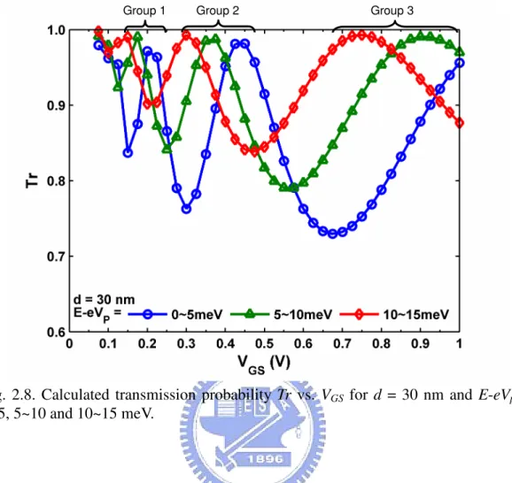
to 56 K………...34 Fig. 2.8 Calculated transmission probability Tr vs. VGS for d = 30 nm and E-eVp =
Fig. 2.9 Measured GDS and Gm'/VDS vs. (VGS-VT) characteristics for the
non-overlapped Device 2 with Lg = 30 nm and Wfin = 25 nm at VDS = 1 and
50 mV under T = 56 and 300 K. (Gm' = ∂Gm/∂VGS and Gm =
∂IDS/∂VGS)………...36
Fig. 2.10 Calculated transmission probability Tr vs. VGS and E for d = 30 nm……37
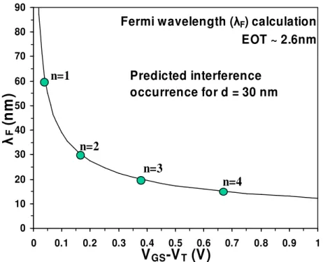
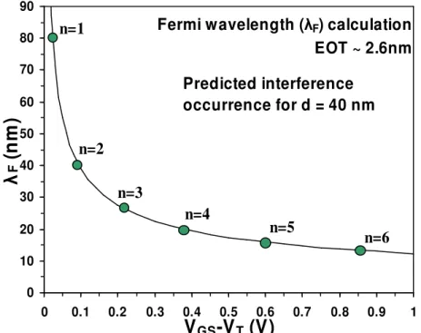
Fig. 2.11 Fermi wavelength as a function of (VGS-VT). The location at which the
quantum interference occurs is indicated for d = 30 nm………...38 Fig. 2.12 Fermi wavelength as a function of (VGS-VT). The location at which the
quantum interference occurs is indicated for d = 40 nm………...39 Fig. 2.13 Calculated transmission probability Tr vs. VGS and E for d = 40 nm……40
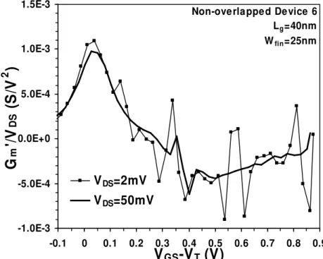
Fig. 2.14 Measured Gm'/VDS vs. (VGS-VT) characteristics for the Device 6 with Lg =
40 nm and Wfin = 25 nm……….…....41
Fig. 2.15 Illustration of the quantum interference effect on ID–VGS, Gm–VGS, and
∂Gm/∂VGS vs. VGS characteristics………42
Fig. 2.16 AC Gm measurement used in this work (freq. = 2 MHz). Note that the
trapping/de-trapping mechanisms can be suppressed by the AC
method………...43 Fig. 2.17 DC and AC measurement results of ∂Gm/∂VGS vs. VGS-VT for the Device 4
with Lg = 30 nm and Wfin = 25 nm. We can determine the (VGS-VT) at
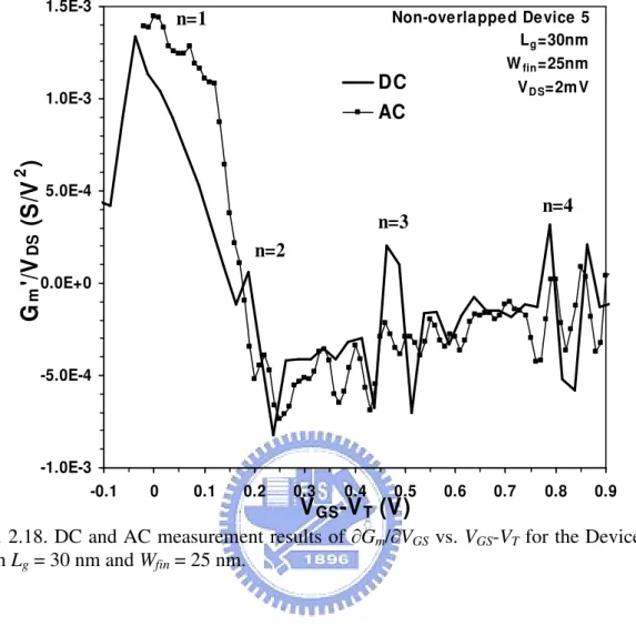
which quantum interference occurs for each n (indicated by arrows)…...44 Fig. 2.18 DC and AC measurement results of ∂Gm/∂VGS vs. VGS-VT for the Device 5
with Lg = 30 nm and Wfin = 25 nm……….……45
Fig. 2.19 Extracted VGS-dependent Leff for the non-overlapped multiple-gate
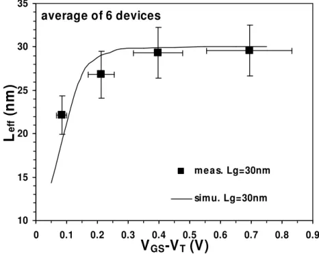
FinFETs with Lg = 30 nm and Wfin = 25 nm……….….46
Fig. 2.20 A schematic carrier density plot along the channel between source and
drain for the non-overlapped gate to source/drain structure at VGS = 0 to 1
V. Leff is determined based on the inversion-layer sheet
Chapter 3
Fig. 3.1 Schematic of a quantum dot, in the shape of an island, connected to source
and drain electrodes by tunnel barriers and to a gate by a capacitor
(Cg)……….………66
Fig. 3.2 An illustration of Coulomb blockade oscillations, the effect of single
electron charges on the conductance vs. VG characteristics. The period in
gate voltage VG is about e/Cg. VG3 > VG2 > VG1.………..…..67
Fig. 3.3 An example of Coulomb blockade oscillations in GDS vs. VG
characteristics. The conductance GDS is the ratio IDS/VDS and the period
∆VG is about e/Cg………...68
Fig. 3.4 Multiple-gate Fin-FET SOI structure investigated in this work and (b) its cross-sectional view along A-A’ view showing the non-overlapped gate to
source/drain regions. (c) A schematic electronic potential plot along the
channel between source and drain for the FinFET with non-overlapped
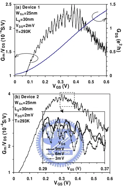
regions……….………..69 Fig. 3.5 Periodic oscillations occur in Gm/VDS vs. VGS characteristics for (a) the
Device 1 and (b) the Device 2 with Lg = 30 nm and Wfin = 25 nm at T =
293K………..70 Fig. 3.6 Periodic oscillations occur in dGm (= Gm-<Gm>) vs. VGS characteristics for
the Device 1 at (a) T = 293 K and (b) T = 233 K. <Gm> is the long-range
average……….…..71 Fig. 3.7 Both (a) the FFT and (b) the histogram of the directly counted
peak-to-peak spacing (∆VG) confirm that the period (<∆VG>) in Fig. 3.6 is
17 mV………72 Fig. 3.8 Periodic oscillations occur in Gm/VDS vs. VGS characteristics for the Device
3 with Lg = 40 nm and Wfin = 25 nm at T = 20 oC. Smaller peak-to-peak
spacing (∆VG = 15 mV) from the FFT can be seen………...73
Fig. 3.9 Periodic oscillations occur in dGm vs. VGS characteristics for the Device 4
with Lg = 40 nm and Wfin = 15 nm at (a) VGS = 0~0.2 V, (b) VGS = 0.2~0.4
V and (c) VGS = 0.4~0.6 V. (d) The FFT of periodic oscillations in
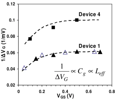
Fig. 3.10 VGS dependence of 1/<∆VG> can be observed for the Device 1 and 4.
<∆VG> is extracted from the FFT in different VGS regimes………….…..75
Fig. 3.11 An illustration of the VGS-modulated tunnel barriers……….76
Fig. 3.12 Periodic oscillations occur in dGm vs. VGS characteristics for the Device 5
with Lg = 30 nm, Wfin = 25 nm and NB = 3×1018 cm-3 at (a) VGS = -0.8~-0.6
V and (b) VGS = -0.6~-0.4 V. (c) The FFT of periodic oscillations in
different VGS regimes……….77
Fig. 3.13 Periodic oscillations occur in dGm vs. VGS characteristics for the Device 6
with Lg = 40 nm, Wfin = 25 nm and NB = 3×1018 cm-3 at VGS = 0~0.3 V. (b)
The FFT of periodic oscillations in different VGS
regimes……….…..78 Fig. 3.14 Periodic oscillations occur in dGm vs. VGS characteristics for the Device 7
with Lg = 30 nm and Wfin = 25 nm at (a) T = 293 K and (b) T = 56
K………79 Fig. 3.15 Schematic energy diagram of a SET. The quantum energy levels are
discrete with each quantum-level spacing defined as ∆ε. ∆E is the
charging energy e2/CΣ………....80
Fig. 3.16 Periodic oscillations occur in dGm vs. VGS characteristics for the Device 8
with Lg = 40 nm and Wfin = 25 nm at (a) VDS = 0.3 mV and (b) VDS = 10
mV under T = 56 K………81 Fig. 3.17 (a) Rhombus diagram for the Device 2. (b) dGm vs. VGS characteristics at
VDS = 2 mV. The conductance peaks (dots) correspond to the dots at VDS =
2 mV in (a)……….82 Fig. 3.18 Rhombus diagram for the Device 3 with Lg = 40 nm and Wfin = 25
nm……….……….83 Fig. 3.19 Measured junction capacitance Cj per unit width vs. VBS characteristics for
planar SOI NMOSFET with high and low doping………....84 Fig. 3.20 Cg vs. Lg characteristics for different extraction methods……….…85
Chapter 4
Fig. 4.1 Schematic diagram illustrating the backscattering theory [1]. Carrier in the
critical length l is with a backscattering ratio rsat. The average injection
velocity υinj is determined the equilibrium thermal velocity υtherm and rsat as
υinj = υtherm(1-rsat)/(1+rsat) ………110
Fig. 4.2 Calculated ballistic efficiency B vs. Lg based on the results of [20]
showing the need of accurate VT,sat and (βµ-βl) ………...111
Fig. 4.3 Measured Id,sat and VT,sat vs. T characteristics for the NMOSFET with Lg =
120 nm. Linear dependence of Id,sat and VT,sat on T is shown for T = 233 ~
373 K. VT,sat is determined by maximum transconductance method with
DIBL considered, i.e., VT,sat = VT,lin-DIBL……….…...112
Fig. 4.4 Different estimations of -(∂VT/∂T)/(Vgs-VT). VT,lin is extrapolated from the
maximum transconductance. DIBL is the gate-voltage difference between
gate voltages at Id = 100 nA/µm for Vds = 0.05 and 1.5 V………..113
Fig. 4.5 λ/l vs. T characteristics shows the need of self-consistent β for the backscattering coefficient extraction. In [7]-[15], β = -1.5 from β =
1+(βµ-βl), βµ = -1.5 and βl = 1. Note that different values of Id,sat and VT,sat
are considered in (4) at the corresponding temperature………..114 Fig. 4.6 Extracted β and βµ vs. Vgs characteristics for the NMOSFET with Lg = 120
nm. βµ (–□–) is observed based on the effective mobility µ, which is
extracted at different temperature by the split C–V method with Rsd
correction……….115 Fig. 4.7 Extracted β vs. Lg characteristics for NMOSFETs at VGS-VT,sat = 0.9 V.
The self-consistently extracted β shows significant Lg
dependence….……….116 Fig. 4.8 Extracted rsat and the effective mobility µ vs. Vgs characteristics for the
NMOSFET with Lg = 120 nm……….117
Fig. 4.9 Extracted rsat vs. Vgs characteristics for the NMOSFET with Lg = 120 nm
with different ∆γ corrections………...118 Fig. 4.10 (a) Extracted β and (b) rsat vs. (Vgs-VT,sat) characteristics for 100-nm-Lg
Fig. 4.11 (a) Extracted β and (b) rsat vs. (Vgs-VT,sat) characteristics for 100-nm-Lg
NMOSFETs with HfO2 and SiO2 gate dielectrics………..120
Fig. 4.12 Measured drain-current vs. gate voltage characteristics for 50-nm-Lg
PMOSFETs with and without uniaxially compressive strain at T = 233,
298, 373 K for (a) |Vds| = 0.05 V and (b) |Vds| = 1.3 V………....121
Fig. 4.13 (a) Extracted β and (b) rsat vs. |Vgs-VT,sat| characteristics for 50-nm-Lg
PMOSFETs with and without uniaxially compressive strain [23][24]. The
Rsd effect has been corrected. (Rsd ~ 125 Ω/um for the strained device and
214 Ω/um for the unstrained device)………..122 Fig. 4.14 Extracted (a) thermal velocity υtherm, (b) mean-free path λ and (c) effective
mobility µ vs. |Vgs-VT| characteristics for 50-nm-Lg PMOSFETs with and
without uniaxially compressive strain at T = 298 K. λ is extracted from the
slop of Id,lin–Vds characteristics at Vds = -20 ~ 20 mV. Effective mobility is
extracted from the split C–V method at Vds = 50 mV with Rsd correction
[2]………123 Fig. 4.15 Extracted potential -kBT/q vs. (lT-l233K) characteristics for (a) strained and
unstrained PMOSFETs with Lg = 50 nm at |Vgs-VT,sat| = 0.8 V and |Vds| =
1.3 V, and (b) the strained PMOSFET with Lg = 50 nm at |Vgs-VT,sat| = 0.4
~ 0.8V and |Vds| = 1.3 V………..124
Fig. 4.16 Our self-consistent method considering accurate temperature dependence
of carrier mobility and self-heating effects……….125 Fig. 4.17 Self-heating induced ∆T vs. ambient temperature T0 for the SOI MOSFET
with Lg = 63 nm. Rth (= 67064 K/W) is extracted by the method presented
in [34]………..126 Fig. 4.18 λ/l vs. T characteristics for (a) the constant β = -1.5 (i.e., βµ = -1.5 and βl =
1) and the self-consistent β, and (b) the self-consistent β with and without
the correction of self-heating………...127 Fig. 4.19 rsat vs. Vgs characteristics for SOI NMOSFETs with Lg = 216 nm and 63
nm using the conventional method (i.e., assuming β = -1.5 in (10))……128 Fig. 4.20 rsat vs. Vgs characteristics for SOI NMOSFETs with Lg = 216 nm and 63
Fig. 4.21 Gds and the extracted β vs. Vds characteristics for SOI NMOSFET with Lg
= 216 nm and 63 nm. The floating-body effects can be seen in both Gds
and the self-consistently extracted β………130 Fig. 4.22 Comparison of σ(VT) and σ(VT)/VT for strained and unstrained
PFETs………..131 Fig. 4.23 σ(Id,sat)/Id,sat vs. σ(µ0)/µ0 characteristics for strained and unstrained PFETs
with Lg = 50 ~ 500 nm at Vds = 1.3 V………..132
Fig. 4.24 Bsat enhancement and µ enhancement vs. Lg characteristics for strained and
unstrained PFETs. Bsat: ballistic efficiency B in saturation
region………...133 Fig. 4.25 Vds dependence of the ballistic-efficiency enhancement. B is near λ/(2l+λ)
for high Vds and λ/(Lg+λ) for low Vds………...134
Fig. 4.26 σ(Id)/Id vs. σ(µ0)/µ0 characteristics for strained and unstrained PFETs with
Lg = 50 ~ 500 nm at Vds = 0.3 V………..135
Chapter 5
Fig. 5.1 (a) Inversion MOS capacitance (Cgc) for the short-channel (Lg = 0.24µm)
device. C0: true capacitance for Lg = 10 µm. (b) The variation of Cm
increases as Lg decreases. Cm: measured capacitance. <Cm>: Cm
mean………148 Fig. 5.2 (a) The impact of cable inductance, Ls, on Cgc. (b) Frequency dependence
of the measured Cgc……….149
Fig. 5.3 (a) BSIM4-based macro model. Cf: fringing capacitance. R4 = 1x10⁹ Ω, C4
= 1x10⁻⁹ F. (b) Our BSIM4 extraction methodology of the inversion MOS
capacitance………..150 Fig. 5.4 (a) Merely considering Rge and Rsd without taking Li into account cannot
model the Cgc characteristics in the high gate bias regime. (b) In the same
MOS array of short-channel devices, the impact of on-chip inductance (Li)
depends on the measurement configuration. (For the SD-G case, the Hi
electrode.)………152 Fig. 5.5 The segmented SPICE simulation reveals the importance of calibrations
and the distributed effect for the long channel device………153 Fig. 5.6 The cable inductance Ls vs. frequency characteristics. ~1µH Ls can be
excluded after performing the SHORT calibration……….154 Fig. 5.7 (a) DC and (b) AC verification of the segmented SPICE simulation for the
distributed effect……….…….155 Fig. 5.8 (a) The gate-tunneling induced C–V attenuation due to de-biasing effect
can be simulated by BSIM4/SPICE simulation. (b) The gate currents
simulated by the segmented simulation and the Rii lumped simulation are
nearly identical. (c) Segmented SPICE simulation with each sub-transistor
modeled by the BSIM4 MOSFET model. (d) Single-transistor SPICE
simulation with Rii added to the gate terminal in addition to
Rge………156
Fig. 5.9 (a) Rii for Lg = 10 µm device can be extracted from the DC output
characteristics. (b) Rii as a function of VGS and Lg………...158
Fig. 5.10 Small-signal equivalent models for MOS capacitor. (a) Three-element
model. (b) Two-element parallel model………..159 Fig. 5.11 Reconstructed C–V characteristics for (a) NMOS and (b) PMOS with and
without considering Rii. The results agree well with the simulation results
of NCSU CVC. (TOX = 1.15 nm. NMOS : NBulk = 3E17 cm-3, NGate =
1.8E20 cm-3, Rge+Rsd/2 = 40 Ω. PMOS : NBulk = 2.5E17 cm-3, NGate =
8.5E19 cm-3, Rge+Rsd/2 = 180 Ω.)………160
Fig. 5.12 The contribution of intrinsic input resistance in the overall gate-current
Chapter 1
Introduction
1.1 Background and motivation
Regarding conventional silicon metal-oxide-semiconductor field-effect transistors (MOSFETs), the device size is scaled in all dimensions, resulting in smaller oxide thickness, channel length, and channel width. Currently, 45 nm (with a physical gate length ~30 nm) is the state-of-the-art process technology, but even smaller dimensions are expected in the future [1]. For example, bulk silicon MOSFETs with the 10-nm physical gate length have been demonstrated by the Intel Corporation [2]. As the device size is scaled, not only device speed (i.e., circuit performance) is enhanced but also the cost and the consuming power can be reduced. To continue the scaling trend, multiple-gate silicon-on-insulator (SOI) MOSFETs are considered as a promising candidate for ultra-scaled complementary metal-oxide-semiconductor (CMOS) devices [3]. It has been reported that excellent subthreshold characteristics can be achieved in the nanowire FinFET with the 5-nm physical gate length [4].
It is important to point out that the exponential growth in integrated circuit complexity, which has seen a hundred-million-fold increase in transistor count per chip over the past forty years, will be finally facing its limits. One reason is that critical dimensions, such as transistor gate length Lg and oxide thickness tox, are reaching
physical limitations. Besides, maintaining dimensional integrity at the limits of scaling is also a challenge. Although these manufacturing issues may be overcome by introducing novel materials (e.g., high-k dielectric, germanium channel) or
performance enhancement, fundamental device-physics issues may still restrict the device performance enhancement [5]. Several examples are listed as follows:
First, it has been presented in [6] that quantum-mechanical tunneling current from the source to the drain may limit the device performance for ultra-scaled-Lg
devices. The insensitive temperature dependence of subthreshold characteristics indicating the tunneling current between the source to the drain was observed for the 8-nm-Lg MOSFET [6]. Such a tunneling current is starting to dominate instead of the
thermal current and makes it difficult to obtain sufficiently high on/off current ratio when Lg is reduced.
Besides, significant quantum-mechanical tunneling current through the gate dielectric drastically increases with thinning oxide thickness [6]. The consequences are not only the increasing stand-by power dissipation but also the distorted capacitance-voltage (C−V) characteristics [7]. Note that C−V measurements are a fundamental characterization technique for MOS devices. Accurate determination of device capacitance is critical for oxide thickness extraction [8], metallurgical channel length determination [9], mobility measurement [10] and interface trap characterization [11].
Quantum-mechanical confinement effects are expected for the size smaller than 15 nm and may impact carrier transport. In [12], evidence of one-dimensional subband formation was observed at low temperature in tri-gate SOI MOSFETs, resulting in oscillations of current-voltage characteristics. It is worth noting that such quantum-mechanical effects on current-voltage characteristics can directly impact carrier mobility at room temperature [13]. The inter-subband scattering significantly affects the carrier mobility and results in the negative resistance and the dynamic mobility behavior.
For nanoscale MOSFETs with effective channel length so short comparable to de Broglie wavelength, the quantum interference phenomenon stemmed from the wave nature of channel electrons can occur and impact the transistor characteristics [14]. Strictly speaking, quantum interference occurs when device size and elastic scattering length are smaller than or approximately equal to the “phase coherence length” (i.e., inelastic scattering length) of carriers. This phase coherence length is the distance a carrier travels before it encounters a phase-randomizing collision, which effectively destroys its quantum mechanical wave nature and restores classical (particle-like) behavior [15]. The wave nature of carriers will give rise to conductance fluctuation due to the elastic scattering center, such as trapped charges [14], ionized atoms [16], electric potential barriers [17]. Besides, when the quantum interference prevails, the Anderson localization effect can result in conductance loss [18].
Moreover, the single-electron effect due to Coulomb blockade may also become increasingly significant with scaling CMOS devices because the number of charges in such small size is rare [19]. The phenomenon of single-electron tunneling was first predicted by Russians scientist Likharev in 1986 for a small tunnel junction, which is essentially a small capacitor with a capacitance C. For the small capacitor, the charge Q and the corresponding charging energy ∆E are discrete and relate to C as ∆E = Q2/2C [20]. Carrier transport through such a small capacitor is determined by the discrete ∆E and shows periodic oscillations in current-voltage characteristics. Due to the innovation of semiconductor technology, the studies of single-electron phenomena associated with tunneling in semiconductor nanostructures [21], bulk CMOS devices [22], SOI MOSFETs [23] and nano dots [24] have emerged.
Furthermore, the continuous scaling down of MOSFETs has made possible to realize devices with Lg comparable to the carrier transport mean-free-path. In these
structures, carrier motion can be ballistic [25][26], i.e., a carrier can traverse the entire structure from one end to the other without suffering any collision with other carriers, elastic centers, and inelastic phonon. When this happens, the motion of carriers can not be described adequately by the concept of the effective mobility. In [27], the convenience of the effective mobility was challenged especially for a nanoscale MOSFET under high drain bias where off-equilibrium transport dominates. Besides, the performance of nano-scaled devices becomes more complicated to predict just relying on the concept of the effective mobility [28].
From the above examples one may say that the amazing progress of CMOS technology leads to a significant evolution of the mechanisms of carrier transport in nanoscale MOSFETs, and may also affect the basic principles of device scaling and optimization. Therefore, the purpose of this thesis is to explore further into mechanisms of carrier transport in nanoscale MOSFETs as well as to investigate innovative applications based on state-of-the-art CMOS devices.
In addition to manufacturing and fundamental device-physics issues, there is still a challenging task to characterize important device parameters (e.g., Lg and gate
capacitance Cg) of nanoscale MOSFETs using conventional extraction methods
(top-down approaches). For example, the applicability of conventional effective channel length Leff extraction methods [29][30] is questioned because of the non-ohmic
gate-underlap [31]. Moreover, the geometry-dependent parasitics associated with the 3-D topography of nonplanar devices [32] may result in difficulty in the observation of intrinsic Cg by traditional C−V based measurements. Therefore, the feasibility of using
the mesoscopic phenomena (buttom-up approaches) to determine important device parameters for nanoscale MOSFETs merits investigation.
1.2 Organization
This dissertation includes six chapters.
In Chapter 1, the background and the motivation of this thesis are reviewed. In Chapter 2, we conduct a systematic comparison of carrier transport between overlapped and non-overlapped multiple-gate SOI MOSFETs (MuGFETs). The classical current-voltage and mesophysical characteristics have been investigated for devices with effective channel length Leff = 50 to 60 nm and fin width Wfin = 5 to 25 nm at T =
300 to 56 K. Several mesophysical characteristics, including quantum-mechanical confinement effects [12][13], quantum-mechanical interference effects [33], single-electron effects [34], variable range hopping conductance [25] and universal conductance fluctuations [35], are systematically examined. In addition, a new approach of Leff extraction is developed based on the quantum-mechanical interference effects.
In Chapter 3, we further demonstrate controlled single-electron effects in the non-overlapped MuGFETs [34] through a comprehensive investigation for the observed single-electron effects. Then, we systematically present single-electron effects for devices with various gate length (Lg), fin width (Wfin), gate bias (VGS), body doping (NB)
and temperature [36]. The impact of access resistances [23], the estimation of gate-dot coupling strength [37] and phenomena of split-peak separations [38] are discussed. Besides, we demonstrate that the gate capacitance as well as source/drain capacitance can be extracted with an aF-scale resolution by single-electron effects.
In Chapter 4, we report a generalized temperature-dependent channel backscattering extraction method that can self-consistently determine the temperature sensitivity of low-field mobility (µ0)and the critical length (l) in nanoscale MOSFETs
[39]-[40]. The validity of our method for the process monitoring purpose is assessed based on various types of devices: high vs. low body-doping, HfO vs. SiO dielectric,
and unstrained vs. uniaxially strained devices. Through the extracted channel backscattering coefficients, we investigate the impacts of the Coulomb scattering, the uniaxial strain, the self-heating effect and the floating-body effect on ballistic efficiency. Finally, we propose that the drain current variation can be suppressed through enhanced ballistic efficiency.
In Chapter 5, we systematically examine the gate tunneling current induced C−V distortion from measurements to simulations. Through the BSIM4-based macro model, different mechanisms of C−V distortion can be characterized for short and long channel devices. Then, we investigate the validity of the concept of intrinsic input resistance [41] in the characterization of the distributed channel RC effects [42]. Finally, we assess the feasibility of using the intrinsic input resistance approach for the inversion C−V reconstruction [43].
Chapter 6 summarizes essential research results and contributions of this dissertation work.
References
[1] International Technology Roadmap for Semiconductors, 2007, [Online]. Available: http://www.itrs.net/Links/2007ITRS/Home2007.htm.
[2] R. Chau, B. Boyanov, B. Doyle, M. Doczy, S. Datta, S. Hareland, B. Jin, J. Kavalieros, and M. Metz, “Silicon nano-transistors for logic applications,” Physica E: Low-dimensional Systems and Nanostructures, vol. 19(1–2), pp. 1–5, July 2003.
[3] Z. Krivokapic, C. Tabery, W. Maszara, Q. Xiang, and M.-R. Lin, “High performance 45 nm CMOS technology with 20 nm multi-gate devices” 2003 Int. Conf. Solid State Devices Materials, pp. 760–61, 2003
[4] F.-L. Yang, D.-H. Lee, H.-Y. Chen, C.-Y. Chang, S.-D. Liu, C.-C. Huang, T.-X. Chung, H.-W. Chen, C.-C. Huang, Y.-C. Yeo, Y.-M. Li, J.-W. Lee, P. Chen, M.-S. Liang, and C. Hu, “5nm-Gate Nanowire FinFET,” Symp. VLSI Tech. Dig., pp. 196–197, June 2004.
[5] H.-S. Philip Wong, “Beyond the conventional transistor,” IBM J. of Research and Development, vol. 46(2–3), pp. 133–168, 2002.
[6] M. Fukuma, “New Frontiers of Sub-100nm VLSI Technology - Moving toward Device and Circuit Co-design,” Symp. VLSI Tech. Dig., pp. 4–5, 2000.
[7] K. J. Yang and C. Hu, “MOS Capacitance Measurements for High-Leakage Thin Dielectrics,” IEEE Trans. on Electron Devices, vol. 46(7), pp.1500–1501, July 1999.
[8] S.-H. Lo, D.A. Buchanan, Y. Taur, and W. Wang, “Quantum mechanical modeling of electron tunneling current from the inversion layer of ultra-thin-oxide nMOSFET’s,” IEEE Electron Device Letters, vol. 18(5), pp. 209–211, May 1997. [9] S.-W. Lee, “A capacitance-based method for experimental determination of
metallurgical channel length in submicron LDD MOSFET’s,” IEEE Trans. on Electron Devices, vol. 41(3), pp. 403–412, Mar. 1994.
[10] C.-L. Huang, J.V. Faricelli, and N.D. Arora, “A new technique for measuring MOSFET inversion layer mobility,” IEEE Trans. on Electron Devices, vol. 40(6), pp. 1134–1139, June 1993.
[11] A. Koukab, A. Bath, and E. Losson, “An improved high-frequency C−V method for interface state analysis on MIS structures,” Solid-State Electron., vol. 41(4), pp. 634–641, 1997.
[12] J.-P. Colinge, A.J. Quinn, L. Floyd, G. Redmond, J.C. Alderman, W. Xiong, C.R. Cleavelin, T. Schulz, K. Schruefer, G. Knoblinger, and P. Patruno,
“Low-temperature electron mobility in Trigate SOI MOSFETs,” IEEE Electron Device Letters, vol. 27(2), pp. 120–122, Feb. 2006.
[13] J.-P. Colinge, W. Xiong, C.R. Cleavelin, T. Schulz, K. Schrufer, K. Matthews, and P. Patruno, “Room-Temperature Low-Dimensional Effects in Pi-Gate SOI MOSFETs,” IEEE Electron Device Letters, vol. 27(9), pp. 775–777, Sept. 2006. [14] A. Ohata, A. Toriumi, and J. Koga, “A study of quantum interference fluctuations
in deep sub-µm MOSFET's under cryogenic conditions”, IEEE Trans. on Electron Devices, vol. 41(11), pp. 2107–2111, Nov. 1994.
[15] M. Cahay and S. Bandyopadhyay, “Semiconductor quantum devices,” IEEE Potentials, vol. 12(1), pp. 18–23, Feb. 1993.
[16] M.J. Gilbert and D.K. Ferry, “Quantum interference in fully depleted tri-gate quantum-wire transistors-the role of inelastic scattering,” IEEE Trans. on Nanotechnology, vol. 4(5), pp. 599–604, Sept. 2005.
[17] H. Ueno, M. Tanaka, K. Morikawa, T. Takahashi, M. Miura-Mattausch, and Y. Omura, “Origin of transconductance oscillations in silicon-on-insulator metal-oxide-semiconductor field-effect transistors with an ultrathin 6-nm-thick active Si layer,” J. Applied Physics, vol. 91(8), pp. 5360–5364, Apr. 2002.
[18] P.W. Anderson, “Absence of Diffusion in Certain Random Lattices,” Phys. Rev., vol. 109(5), pp. 1492–1505, 1958.
[19] K.K. Likharev, “Single-Electron Devices and Their Applications”, Proceedings of The IEEE, vol. 87(4), pp.606–632, April 1999.
[20] I.G. Neizvestnyi, O.V. Sokolova, and D.G. Shamiryan, “Single electronics,” Russian Microelectronics, vol. 28(2), pp. 67–88, 1999.
[21] U. Meirav and E.B. Foxman, “Single-electron phenomena in semicoductors,” Semicond. Sci. Technol., vol. 11, pp. 255–284, 1996.
[22] F. Boeuf, X. Jehl, M. Sanquer and T. Skotnicki, “Controlled Single-Electron Effects in Nonoverlapped Ultra-Short Silicon Field Effect Transistors,” IEEE Trans. on Nanotechnology, vol. 2(3), pp.144–148, Sept. 2003.
[23] X. Jehl, M. Sanquer, G. Bertrand, G. Guégan, S. Deleonibus, and D. Fraboulet “Silicon Single Electron Transistors With SOI and MOSFET Structures: The Role of Access Resistances,” IEEE Trans. on Nanotechnology, vol. 2(4), pp.308–313, Dec. 2003.
[24] L. Zhuang, L. Guo, and S. Y. Chou, “Silicon single-electron quantum-dot transistor switch operating at room temperature,” Appl. Phys. Letters, vol. 72(10), pp.1205–1207, March 1998.
[25] K. Natori, “Ballistic metal-oxide-semiconductor field effect transistor,” J. Appl. Phys., vol. 76(8), pp. 4879–4890, Oct. 1994.
[26] M.S. Lundstrom, “Elementary scattering theory of the Si MOSFET,” IEEE Electron Device Letters, vol. 18(7), pp. 361–363, July 1997.
[27] M.S. Lundstrom, “On the mobility versus drain current relation for a nanoscale MOSFET,” IEEE Electron Device Letters, vol. 22(6), pp. 293–295, June 2001. [28] M.-H. Liao, C.-W. Liu, Lingyen Yeh, T.-L. Lee, and M.-S. Liang, “Gate width
dependence on backscattering characteristics in the nanoscale strained complementary metal-oxide-semiconductor field-effect transistor,” Appl. Phys. Letters, vol. 92(6), p. 063506, Feb. 2008.
[29] D.J. Mountain, “Application of electrical effective channel length and external resistance measurement techniques to a submicrometer CMOS process,” IEEE Trans. on Electron Devices, vol. 36(11), pp. 2499–2505, Nov. 1989.
[30] G.J. Hu, C. Chang, and Y.-T. Chia, “Gate-voltage-dependent effective channel length and series resistance of LDD MOSFET's,” IEEE Trans. on Electron
Devices, vol. 34(12), pp. 2469–2475, 1987.
[31] J.G. Fossum, M.M. Chowdhury, V.P. Trivedi, T.-J. King, Y.-K. Choi, J. An, and B. Yu, “Physical insights on design and modeling of nanoscale FinFETs,” IEDM Tech. Dig., pp. 29.1.1–29.1.4, 2003.
[32] W. Wu and M. Chan, “Analysis of Geometry-Dependent Parasitics in Multifin Double-Gate FinFETs,” IEEE Trans. on Electron Devices, vol. 54(4), pp. 692–698, April 2007.
[33] W. Lee and P. Su, “A Comparative Study of Carrier Transport for Overlapped and Non-overlapped Multiple-Gate SOI MOSFETs,” IEEE Trans. on Nanotechnology, 2009, to be published.
[34] W. Lee, P. Su, H. Chen, C. Chang, K. Su, S. Liu, and F. Yang, “An Assessment of Single-Electron Effects in Multiple-Gate SOI MOSFETs with 1.6-nm Gate Oxide near Room Temperature,” IEEE Electron Device Letters, vol. 27(3), pp. 182–184, March 2006.
[35] G. Wirth, U. Hilleringmann, J. T. Horstmann, and K. Goser, “Mesoscopic transport phenomena in ultrashort channel MOSFETs,” Solid-State Electronics, vol. 43(7), pp. 1245–1250, July 1999.
[36] W. Lee and P. Su, “Single-electron effects in non-overlapped multiple-gate silicon-on-insulator metal-oxide-semiconductor field-effect transistors,” Nanotechnology, vol. 20, p. 065202, Feb. 2009.
[37] Y.-M. Wan, K.-D. Huang, C.-L. Sung, and S.-F. Hu, “Transport properties of ultra thin oxide gated Si SET near room temperature,” Proc. 5th IEEE Conf. Nanotechnology, vol. 2, pp.750–753, July 2005.
[38] F.R. Waugh, M.J. Berry, D.J. Mar, and R.M. Westervelt, “Single-electron charging in double and triple quantum dots with tunable coupling,” Phys. Rev. Letters, vol.
75(4) pp.705–708, July 1995.
[39] W. Lee and P. Su, “Investigation of Channel Backscattering Characteristics in Nanoscale Uniaxial Strained PMOSFETs,” IEEE Trans. on Nanotechnology, 2009, to be published.
[40] W. Lee and P. Su, “Investigation of Channel Backscattering Characteristics for Nanoscale SOI MOSFETs Using a New Temperature-Dependent Method,” Proc. 2008 IEEE Int. SOI Conf., New York, USA, pp. 73–74, Oct. 2008.
[41] X. Jin, J.-J. Ou, C.-H. Chen, W. Liu, M. J. Deen, P. R. Gray, and C. Hu, “An Effective Gate Resistance Model for CMOS RF and Noise Modeling”, IEDM Tech. Dig., p.961, 1998.
[42] D.W. Barlage, J.T. O’Keeffe, J.T. Kavalieros, M.M. Nguyen, and R. S. Chau, “Inversion MOS Capacitance Extraction for High-Leakage Dielectrics Using a Transmission Line Equivalent Circuit,” IEEE Electron Device Letters, vol. 21(9), pp.454–456, Sept. 2000.
[43] W. Lee, P. Su, K. Su, C. Chiang, and S. Liu, “Investigation of Anomalous Inversion C-V Characteristics for Long-Channel MOSFETs with Leaky Dielectrics: Mechanisms and Reconstruction,” IEEE Trans. on Semiconductor
Chapter 2
Comparison of Carrier Transport for Overlapped and
Non-overlapped Multiple-Gate SOI MOSFETs
2.1 Introduction
Multiple-gate silicon-on-insulator (SOI) MOSFET (MuGFET) structures provide superior electrostatic integrity needed for complementary metal-oxide-semiconductor (CMOS) scaling entering the deca-nanometer regime [1]. The benefits of MuGFET have been extensively investigated regarding issues of short-channel effects (SCE), leakage current, threshold voltage (VT) fluctuations, mobility, and so on [2].
For MuGFET design, source/drain engineering is crucial because of the parasitic drain/source resistance [3] and the parasitic fringing/overlap capacitance that may limit circuit performance [4]. Two options in the source/drain engineering are the overlapped structure with light-doping drain/source (LDD/LDS) and the non-overlapped structure. The LDD/LDS implantation has been widely used in state-of-the-art CMOS devices for suppressing source and drain resistances. On the other hand, transistor optimization for peak circuit performance within leakage current constraints (i.e., minimum CV/I delay) may dictate the non-overlapped gate to source/drain structure to minimize the fringing/overlap capacitance. Whether the various source/drain engineering will impact the carrier transport in nanoscale MuGFETs merits examination. In this chapter, we conduct a systematic comparison of carrier transport between overlapped and non-overlapped MuGFETs. The classical current-voltage and mesophysical characteristics have been investigated for devices with effective channel length Leff = 50
2.2 Overlapped and non-overlapped device structures
The process flow for fabricating MuGFETs is similar to that reported in [32]. Fig. 2.1(a) shows a schematic view of the MuGFET investigated in this study [31]. Our devices were fabricated on SOI wafers using standard CMOS optical lithography [5]. The Si-body thickness, Hfin, was thinned down to about 40 nm by thermal oxidation.
The fin-width, Wfin, was defined by wet etching. After Wfin was developed, the Si-body
fin was doped with BF2 implantation and annealed. Using optical lithography and
anisotropic reactive ion etching, the gate length, Lg, was defined. Note that the
LDD/LDS implantation was performed for the overlapped structure (Fig. 2.1(c)) and was skipped for the non-overlapped structure (Fig. 2.1(b)) before developing the composite spacer of silicon oxide and nitride. Finally, heavily-doped N+ source/drain was made. In this study, we compare these two types of devices based on the same effective source-drain length Leff.
2.3 Experimental comparison
2.3.1
Classical characteristics
Current-voltage measurements (IDS–VGS) at VDS = 50 mV under T = 300 to 56 K
were performed with a 25-mV VGS step for the overlapped Device 1 with Wfin = 25 nm
and Lg = 80 nm (Fig. 2.2), and for the non-overlapped Device 2 with Wfin = 25 nm and
Lg = 30 nm (Fig. 2.3). Fig. 2.2 shows that the subthreshold swing S for the overlapped
Device 1 decreases with temperature. We have confirmed that the S–T characteristic follows the Boltzmann law S = n(kBT/q)ln(10) with the body effect coefficient n ≈ 1.16.
The linear temperature dependence of S is a feature of fully depleted SOI [8], and has also been observed in tri-gate SOI MOSFETs [13].
below 223 K, S is a constant and does not follow the Boltzmann law. This suggests that for the non-overlapped Device 2, tunneling current dominates the fundamental limitation of leakage current instead of the thermal current [12]. We have noted that similar S behavior has been reported at T < 100 K for the planar non-overlapped NMOSFET in [12]. It implies that the leakage current associated with thermionic emission is suppressed in our MuGFET.
The insensitive temperature dependence of IDS can also be found in the strong
inversion region for the non-overlapped Device 2 (Fig. 2.3). In contrast to that of the overlapped Device 1 (Fig. 2.2), the IDS for VGS > 0.6 V is nearly independent on
temperature. These results indicate that carrier transport in the strong inversion region is determined by the phonon-limited mobility for the overlapped Device 1, but not for the non-overlapped Device 2.
2.3.2
Mesophysical characteristics
To further compare the carrier transport characteristics for overlapped and non-overlapped devices, we have investigated channel conductance (GDS = IDS/VDS) with
low VDS. Fig. 2.4 shows the measured GDS versus VGS characteristics for the overlapped
Device 3 with Wfin = 10 nm and Lg = 60 nm. Significant GDS fluctuations can be seen at
T = 56 K (Fig. 2.4(a)). Similar GDS fluctuations have been reported in [6] and attributed
to the intersubband scattering. While the number of populated subbands increases with increasing VGS, the intersubband scattering also increases with each new subband [7]. In
other words, when VGS increases, the GDS increases due to new populated subbands and
then decreases due to the mobility reduction (i.e., the increase of intersubband scattering). Thus, fluctuations can be seen in the GDS–VGS characteristics. We have noted
that the GDS fluctuations almost occur at the same VGS, such as the spike at VGS-VT =
Device 1) with negligible subband splitting, the GDS fluctuations can not be found.
One important criterion to observe the intersubband scattering effect is that the qVDS and kBT are not significantly larger than the subband energy split ∆E [7]. It is
worth noting in Fig. 2.4(a) that the GDS fluctuations can be observed at VDS = 50 mV
under T = 56 K. Considering the voltage drop across the access resistances (i.e., source/drain resistances, contact resistance and back-end metal resistance), the effective qVDS over the channel and therefore ∆E may be about 20 to 30 meV. This is also
consistent that with the observed GDS fluctuations at VDS = 1 mV under T = 223 K
shown in Fig. 2.4(b). Besides, we have noted in our process that the final minimum Wfin
at the channel center is smaller than the mask-defined 10-nm Wfin (final minimum Wfin
~5 nm) due to over etching [31].
An important signature for intersubband scattering is that conductance reductions (i.e., mobility reduction) occur as VDS increases [6]. This is because the drain bias forces
electrons to jump from higher to lower subbands, and thus enhances intersubband scattering and reduces the carrier mobility [7]. It is worth noting that the reductions in GDS due to mobility reduction can also be observed at VDS = 1 mV when temperature
increases from 56 to 223 K. Similar VDS and temperature dependence in GDS has also
been observed for trigate SOI MOSFETs in [6]-[7].
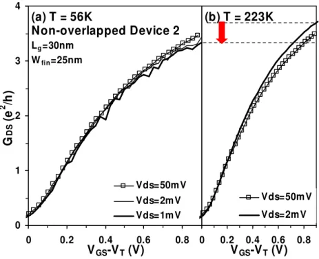
For the non-overlapped Device 2 in the high VGS regime, the GDS increases with
VDS and temperature as can be observed in Fig. 2.5(a) and Fig. 2.5(b), respectively. Such
VDS and temperature dependence of GDS is completely opposite to that of the overlapped
Device 3 (Fig. 2.4) and can not be ascribed to the intersubband scattering effect. In addition, Fig. 2.5 also shows interesting fluctuations with negative differential resistance in the GDS. Although the GDS fluctuations in Fig. 2.5 were observed in the
from the intersubband scattering. In the next section, we shall give more discussions for the anomalous GDS behavior of the non-overlapped Device 2.
2.4 Interpretation
2.4.1
Intersubband scattering effects
As described above, the VDS and temperature dependence of GDS in Fig. 2.5 for
the non-overlapped Device 2 is completely opposite to characteristics of intersubband scattering effect. Therefore, the GDS fluctuations in Fig. 2.5 can not be ascribed to the
intersubband scattering effect. Besides, we have also noted that for the overlapped Device 1 with the same Wfin (i.e., Wfin = 25 nm), the GDS fluctuations can not be found.
2.4.2
Single-electron effects
Coulomb blockade is expected to be important as the charging energy e2/Cg of
the device becomes large [18][19]. With scaling of devices, it is expected that Coulomb blockade oscillation (CBO) occurs in ID–VGS characteristics [20]. Although the
multiple-gate SOI structure with adequate source/drain engineering presents a very promising scheme to build room-temperature SETs [21], we have confirmed in Fig. 2.5 that the physical mechanism described for the non-overlapped device is not due to the CBO. Regarding single-electron effects in the non-overlapped multiple-gate device, we have presented our research results in Chapter 3.
If the GDS–VGS characteristics shown in Fig. 2.5(a) were due to CBO, the VGS
period of CBO can be related to the gate capacitance by e/Cg as well as gate effective
area (Aeff) by Cg = Aeff×εSiO2/EOT. Since the effective oxide thickness (EOT) is about 2.6
nm for our device, from e/Cg ≈ 75 mV (Fig. 2.5(a)), Aeff is estimated ~1.6×10⁻¹² cm2 for
our MuGFET. However, such Aeff is about 15 times smaller than 2HfinLg = 2.4×10⁻¹¹
which is not the signature of CBO.
2.4.3
Variable range hopping conductance
Charged centers in the oxide, interfaces or bulk Si can result in random potential fluctuation [22][23]. In the limit of zero temperature, electron transport is characterized by hopping certain charged centers. When the energy of carriers is increased with temperature or VDS, hopping processes determined by the activation energy may change.
In other words, conductance fluctuations may change with temperature or VDS. This
phenomenon is an origin of the variable range hopping (VRH) itself. In our experimental results, however, the anomalous conductance fluctuations are present at the same (VGS-VT) values for the same device with various temperature and VDS (Fig.
2.9). Besides, if electron transport is limited by the VRH, the tunneling conductance must be less than e2/h [22][23]. That the GDS in Fig. 2.5 is several times e2/h may
exclude the possibility of the VRH. Furthermore, if we assume the anomalous conductance fluctuations are caused by trapping and de-trapping mechanisms, a dependence of fluctuations on the measurement frequency is expected. This could not be observed in our AC Gm measurements in Fig. 2.16 to 2.18.
2.4.4
Universal conductance fluctuations
Due to the two voltage-controlled potential barriers, the universal conductance fluctuations (UCF) [24], as have been predicted by Lee and Stone [25] for disordered systems, are also not expected to be responsible for our observed conductance fluctuations. In addition, to the best our knowledge, the UCF are easily smeared by temperature and may not be easily observed for our devices at T > 4.2 K [26].
2.4.5
Quantum interference effects
as the voltage-controlled potential barriers along the channel. Therefore, carrier transport from source to drain is significantly influenced by the barriers as illustrated in Fig. 2.6: directly tunneling (Ia), thermally-associated tunneling (Ib), and thermionic
emission (Ic). The contribution of these three mechanisms to IDS depends on VGS and
temperature. For high VGS, Ia is dominant. With decreasing VGS, increased electronic
potential diminishes Ia, and thus Ib and Ic become important. In other words, IDS in the
subthreshold region results mainly from Ib and Ic for the non-overlapped device. It is
worth noting that carrier transport by Ic requires more thermal energy and may be
suppressed under low temperature.
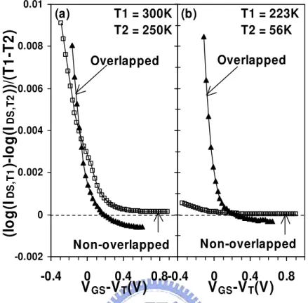
Figure 2.7 shows the temperature sensitivity of IDS (∂log(IDS)/∂T) vs. VGS
characteristics extracted from Fig. 2.2 and Fig. 2.3 under high and low temperatures. For the non-overlapped device in the strong inversion region, the insensitive temperature dependence manifests the importance of Ia. On the other hand, the negative
temperature dependence for the overlapped device in the strong inversion region indicates phonon scattering. In addition, it can be noted in Fig. 2.7(a) that ∂log(IDS)/∂T
significantly increases with decreasing VGS for both overlapped and non-overlapped
devices. This suggests that in the high temperature regime the subthreshold current of the non-overlapped device is dominated by Ic, similar to the overlapped device. When
temperature decreases, however, the thermionic emission Ic is suppressed and the Ib
component with weak temperature dependence becomes dominant. In other words, the suppression of Ic under low temperature is the main reason of S saturation for the
non-overlapped device. It should be noted that such mechanism of S saturation is different from lateral tunneling through the channel, as presented for ultra-short devices in [12] and [17].
non-overlapped device [12]. It is worth noting that the height of the voltage-controlled potential barriers in the non-overlapped regions increases with VGS. The consequence is
the plausibility of electron-wave confined between the barriers. When the length of the quantum well, d, is smaller than the inelastic-scattering (e.g., phonon scattering) length, the phase-coherent electron wavefunction over the entire channel as well as quantum interference between coherent electron waves occur. The quantum interference enhances the electron backscattering probability [9]-[10] and thereby reduces the conductivity expected classically. Such quantum correction to the conductivity is the weak localization effect [9]-[10] and logarithmically dependent on temperature as ∆σ = (pe2/πh)ln(T), where the value of p depends on the scattering process. When T = 56 K, the carriers at VDS = 50 mV experience more heating (more phonon scattering) and thus
less localization effect than those at VDS = 1 or 2 mV. Therefore, the GDS measured at
VDS = 50 mV is larger than that at VDS = 1 or 2 mV (Fig. 2.5). From the GDS data at VDS
= 2 mV under T = 56 K and 223 K in Fig. 2.5, we can estimate that p ≈ 1, which is close to the results in [11] for the 2DEG in Si MOSFETs.
The quantum-mechanical interference for an electron wave passing through a quantum well also results in oscillating transmission probability, Tr, as [14][31]
2 2 2 1 ) sin( ) 2 / ( ) cos( ) exp( d k i d k d ik Tr ω − − = , (1)
where ω = k1/k2 + k2/k1, k1 and k2 are the wave vectors in the non-overlapped region and
in the quantum well, respectively. The wave vectors are determined from
h ) ( 2 1 m E eVp k = − , (2) h ) ( 2 2 m E eVc k = − , (3)