國立交通大學
電信工程學系
碩士論文
應用於 IEEE 802.11a/b/g 之雙頻帶低雜訊放大器和
偶次諧波降頻混頻器以及使用 0.18um CMOS 製作之
Ka 頻低雜訊放大器和 K 頻壓控震盪器
A Dual-Band LNA and a Sub-harmonic Mixer for IEEE 802.11a/b/g
Application and a Ka Band Low Noise Amplifier and a K Band VCO
by Using 0.18um CMOS Process
研究生:張文明
指導教授:周復芳 博士
II
應用於 IEEE 802.11a/b/g 之雙頻帶低雜訊放大器和偶次諧波降頻
混頻器以及使用 0.18um CMOS 製作之 Ka 頻低雜訊放大器和 K 頻壓
控震盪器
A Dual-Band LNA and a Sub-harmonic Mixer for IEEE 802.11a/b/g
Application and a Ka Band Low Noise Amplifier and a K Band VCO
by Using 0.18um CMOS Process
研究生:張文明 Student: Win-Ming Chang
指導教授:周復芳 博士 Advisor: Dr. Christina F. Jou
國 立 交 通 大 學
電 信 工 程 學 系 碩 士 班
碩 士 論 文
A thesis
Submitted to Department of Communication Engineering College of Electrical and Computer Engineering
National Chiao Tung University In Partial Fulfillment of the Requirements
for the Degree of Master of Science in Communication Engineering
June 2006
Hsinchu, Taiwan, Republic of China
I
應用於 IEEE 802.11a/b/g 之雙頻帶低雜訊放大器和偶次諧波降頻
混頻器以及使用 0.18um CMOS 製作之 Ka 頻低雜訊放大器和 K 頻壓
控震盪器
研究生:張文明 指導教授:周復芳 博士
國立交通大學電信工程研究所 碩士班
摘 要
本論文討論應用於射頻接收機的高頻電路設計且主要分為兩個主題探討。其中第ㄧ 部份是增益可調切換式雙頻帶低雜訊放大器及一個新型切換轉導式偶次諧波降頻混頻 器的分析和設計。另ㄧ部份是ㄧ個Ka 頻帶的低雜訊放大器驗證,最後我們以一個 K 頻 帶頻率信號源作為未來的研究專題。 緊接著我們設計並製作ㄧ個使用0.18um CMOS 製程,操作在 2.45GHz/ 5.25GHz 的 增益調整式雙頻帶低雜訊放大器。在高增益模式時,此放大器在2.45-GHz 表現 14.4dB 的功率增益及3.54dB 的雜訊指數。在 5.25-GHz 則有 12.02dB 的功率增益及 2.88dB 的 雜訊指數。此低雜訊放大器在雙頻帶皆有大約11dB 的增益可調範圍, 我們使用0.18um CMOS 製程設計並驗證切換轉導技術的新型偶次諧波降頻混器。 此全整合的次諧波混頻器量測結果顯示使用4dBm 的本地震盪器,在中頻 10MHz 可得 到12.8dB 的降頻轉換功率增益,-1.8dBm 三階諧波交會點,和 14.0dB DSB 雜訊指數。 接下來,ㄧ個使用標準0.18um CMOS 製程的三級 Ka 頻帶低雜訊放大器被製作及驗 證。在32-GHz 時,量測出 12.08dB 的功率增益及 5.325dB 的雜訊指數,總功率消耗為 15.58 毫瓦。 最後,一個使用0.18um CMOS 低相位雜訊 X 頻帶四項位壓控震盪器倍頻而成的 K 頻帶頻率訊號源已被模擬,此K 頻訊號源也當作此論文的將來專題研究II
A Dual-Band LNA and a Sub-harmonic Mixer for IEEE 802.11a/b/g
Application and a Ka Band Low Noise Amplifier and a K Band VCO
by Using 0.18um CMOS Process
Student: Win-Ming Chang Advisor: Dr. Christina F. Jou
Institute of Communication Engineering
National Chiao Tung University
ABSTRACT
This thesis discusses high frequency circuit design for RF receivers and it mainly includes two parts. One is the analysis and design of a switched dual-band LNA with variable gain and a new switched Gm sub-harmonic mixer. The other is the demonstration of a Ka band LNA, and finally a K band frequency source with X band low phase noise quadrature VCO is simulated for feature work.
A switched dual-band low noise amplifier with four gain control modes operating at 2.45-GHz/5.2-GHz has been designed and demonstrated based on a 0.18-um CMOS process. In the high gain mode, the LNA approaches 14.4 dB maximum power gain and 3.54 dB DSB noise figure at 2.45-GHz. In the 5.25-GHz band, the maximum power gain is 12.02 dB and the DSB noise figure is 2.88 dB.
A new prototype of sub-harmonic mixer using switched Gm technique is designed and implemented in a standard 0.18um CMOS technology. This fully integrated sub-harmonic mixer achieves measured high conversion power gain of 12.8 dB, -1.8 dBm IIP3, and 14.0 dB noise figure at 10-MHz with 4 dBm LO power.
A 3-stage Ka band LNA has been designed and verified by using standard CMOS 0.18um process. The measured power gain at 32-GHz is 12.08 dB with noise figure of 5.325 dB while consuming 15.58 mW.
III
Finally, a K band frequency source with X band 0.18um CMOS low phase noise quadrature VCO has been simulated. This K band frequency source is treated as feature work in our thesis.
IV
Acknowledgement
首先,我要感謝指導教授周復芳老師,在這短短兩年的指導及關心,尤
其是在發表國際論文上提供很多寶貴意見且抽空幫學生修改,讓學生在碩
士生涯獲益良多。並且感謝博士班鄭國華學長的耐心指點,在問題重重的
兩年提供我不少研究方向,並在學業上鼓勵及給予信心。
在此要特別感謝系上的高銘盛老師對此論文的細心更改及提供意見,讓
此論文更有深度,且感謝老師在當初進到交大電信系時的指導及方向指
引,讓學生真正在研究路上找到自己的興趣所在。
還有感謝 919 實驗室的博班學長學匯儀,同學宏斌,仕豪,政展,秋榜,
博揚以及學弟妹子豪,宇清,宜星,智鵬,瑞嫻,寶明一起在實驗室的日
子,雖然研究是辛苦的,但是實驗室夥伴的共同闖拼讓這兩年過的相當充
實快樂。
最後謝謝家人的支持,不管事精神上或是實質的供給,讓我無後顧之憂
得順利取得碩士學位,也能諒解我平常假日幾乎回不了家的苦衷。
V
C
ONTENTS
Chinese Abstract I
English Abstract II
Acknowledgement IV
Contents V
List of Tables VII
List of Figures VIII
Chapter 1
INTRODUCTION ... 1
1.1 Background and Motivations ...1
1.2 Thesis Organization...2
Chapter 2
SWITCHED DUAL-BAND LNA WITH FOUR GAIN MODES
AND NEW SWITCHED GM SUB-HARMONIC MIXER... 4
2.1 Introduction ...4
2.2 Comments...5
2.2.1 Switched Dual-Band LNA ...5
2.2.2 Proposed Switched Gm Sub-Harmonic Mixer ...6
2.3 Wireless LAN Standard Review...7
2.3.1 IEEE 802.11a...7
2.3.2 IEEE 802.11b...8
2.3.3 IEEE 802.11g...9
2.4 Circuit Design Consideration ...10
2.4.1 Proposed Dual-Band Receiver...10
2.4.2 Switched Dual-Band LNA ... 11
2.4.2.1 Input Matching ...12
2.4.2.2 Noise Figure ...14
2.4.2.3 Power Dissipation...15
2.4.2.4 The Switched Dual-Band LNA Design Consideration...16
2.4.3 Switched Gm Sub-Harmonic Mixer...19
2.4.3.1 Review of The Gilbert Mixer & Sub-Harmonic Mixer...20
2.4.3.2 Switched Gm Mixer ...24
2.4.3.3 Proposed New Sub-Harmonic Mixer ...25
VI
2.5.1 Switched Dual-Band LNA ...27
2.5.1.1 Measurement Consideration...27
2.5.1.2 Measurement Results and Discussion of Dual-Band LNA ...30
2.5.1.3 Comparison with Other Literatures ...34
2.5.2 Switched Gm Sub-Harmonic Mixer...36
2.5.2.1 Measurement Consideration...36
2.5.2.2 Measurement Results...43
2.5.2.3 Comparison with Other Literatures ...46
Chapter 3
KA BAND LNA USING 0.18μm CMOS... 48
3.1 Introduction ...48
3.2 System Application...49
3.3 Circuit Design...50
3.3.1 Proper Device Size Choice...51
3.3.2 Stability Circle...53
3.3.3 Available Gain Circle ...56
3.3.4 Noise Circle ...57
3.3.5 Inter Stage Matching Network ...63
3.3.6 The simulation results with ideal and on-chip inductors...68
3.4 Measurement Consideration and Results ...73
3.4.1 Measurement Consideration...73
3.4.2 Measurement Results and Discussion ...76
3.4.3 Comparison with Other Literatures ...80
3.5 Conclusion...81
Chapter 4
K BAND FREQUENCY SOURCE WITH X BAND LOW
PHASE NOISE QUADRATURE CMOS VCO... 82
4.1 Introduction ...82
4.2 Circuit Design...83
4.2.1 Quadrature Signal...83
4.2.2 Frequency Doubler ...84
4.2.2.1 Harmonics of Quadrature Signals ...84
4.2.2.2 Pinch-off Clipping ...85
4.2.3 Proposed K Band VCO Architecture...87
4.3 Simulation Results...89
4.4 Comparisons ...93
VII
L
IST
O
F
T
ABLE
Table 1 Comparison of each modulation and its transferring data rate ...8
Table 2 The comparison of the 802.11 a/b/g standards ...9
Table 3 Gain control signal from base band ...19
Table 4 The comparison with published dual-band LNA...34
Table 5 The comparison with the published gain controllable LNA...35
Table 6 The measured forward transmitted S-parameter for each port ...37
Table 7 Summary of the measured results and post-simulation in SS-corner ...46
Table 8 The summary of this work and comparison with other literatures ...47
Table 9 Summary of the LMDS system ...50
Table 10 Single stage performance of the selected Γ ...59 s Table 11 List of each complex reflection coefficient for the designed LNA ...67
Table 12 The pre-simulation and post simulation summary of the proposed LNA..72
Table 13 Summary of the post-simulation and measurement...79
Table 14 Measured results and comparison with other literatures ...80
Table 15 Performance summary of the proposed K band VCO ...93
VIII
L
IST
O
F
F
IGURE
Fig. 2-1 The sub-harmonic mixer used in the proposed dual-band receiver ...8
Fig. 2-2 The North American channel selection of non-overlapping and overlapping ...9
Fig. 2-3 The sub-harmonic mixer used in the proposed dual-band receiver ... 11
Fig. 2-4 The frequency planning in the proposed dual-band LNA ... 11
Fig. 2-5 The input stage of the single band cascade LNA...13
Fig. 2-6 The equivalent series RLC tank of the input matching network ...14
Fig. 2-7 The equivalent series RLC tank of the input matching network ...14
Fig. 2-8 The schematic of the proposed dual-band LNA ...17
Fig. 2-9 M7 is off and the parasitic capacitance, CM7, provides...17
Fig. 2-10 M7 is on and provides a turn on resistance...18
Fig. 2-11 A basic Gilbert Mixer and the waveforms of output IF current ...20
Fig. 2-12 Traditional sub-harmonic mixer and waveforms of output IF current...22
Fig. 2-13 Switched Gm mixer and the waveforms of IF output current ...24
Fig. 2-14 Proposed switched Gm sub-harmonic mixer ...25
Fig. 2-15 Waveform of the switched Gm sub-harmonic mixer ...25
Fig. 2-16 The layout of the proposed switched dual-band LNA ...27
Fig. 2-17 The micrographic of the proposed switched dual-band LNA...28
Fig. 2-18 (a) On-wafer measurement test diagram(b) The photo for measurement environment ...29
Fig. 2-19 Measurement setups for (a)S-parameter (b) noise figure (c)IIP3 and P1dB ...29
Fig. 2-20 The measured S11 of the proposed switched dual-band LNA...30
Fig. 2-21 The measured S22 of the proposed switched dual-band LNA ...31
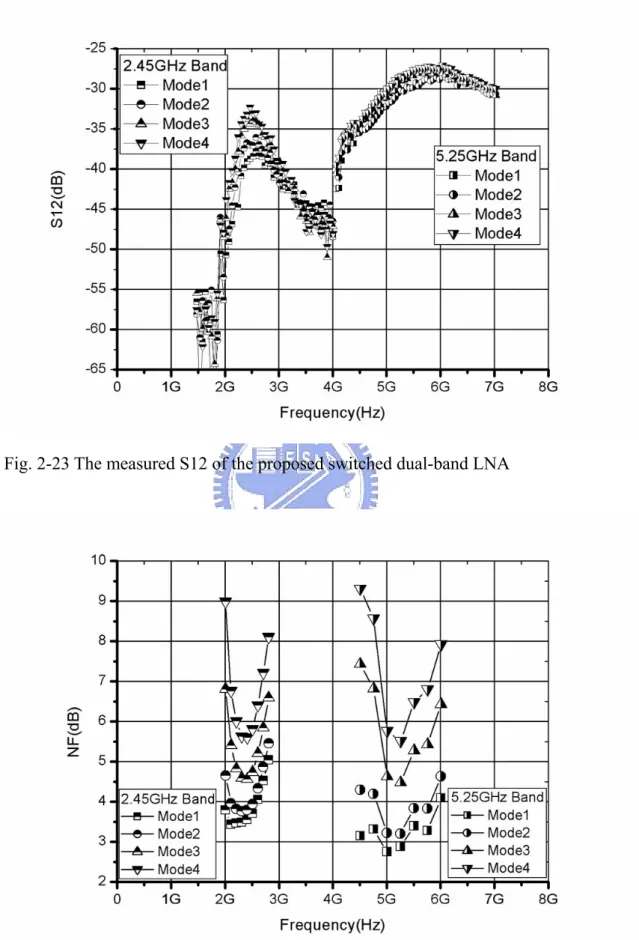
Fig. 2-22 The measured S21 of the proposed switched dual-band LNA ...31
Fig. 2-23 The measured S12 of the proposed switched dual-band LNA ...32
Fig. 2-24 The measured NF of the proposed switched dual-band LNA...32
Fig. 2-25 The measured IIP3 at 2.4-GHz band of the proposed switched dual-band LNA ...33
Fig. 2-26 The measured IIP3 at 5.2-GHz band of the proposed switched dual-band LNA ...33
Fig. 2-27 (a) The LO port quadrature hybrid (b) The LO port rat-race...36
Fig. 2-28 The fabricated LO port quadrature Balun...37
Fig. 2-29 The measured S-parameters for the fabricated quadrature Balun...38
Fig. 2-30 The measured S-parameters for the fabricated quadrature Balun...38
Fig. 2-31 The layout of the proposed sub-harmonic mixer ...39
IX
Fig. 2-33 The die photograph of the switched Gm sub-harmonic mixer ...40
Fig. 2-34 Measurement setup of the proposed switched Gm sub-harmonic mixer for (a) input return loss (b) conversion gain (c) IIP3 and P1dB (d) noise figure ...41
Fig. 2-35 (a) The photo of the PCB test board. (b) (c) The measurement environment in CIC ...42
Fig. 2-36 The simulated and measured RF and LO return loss...44
Fig. 2-37 The simulated and measured conversion power gain against the LO power ...44
Fig. 2-38 The simulated and measured DSB noise figure...45
Fig. 2-39 The simulated and measured third order intercept point (IIP3)...45
Fig. 3-1 Using top metal as the transmission line ...49
Fig. 3-2 Simplified block diagram of a 24-GHz Receiver ...49
Fig. 3-3 Simulation results of f versus VGS... 51 t Fig. 3-4 Simulation results of fmax versus VGS ...51
Fig. 3-5 Simulation of IDS, NFmin , and Gm versus VGS and VDS ...52
Fig. 3-6 Plot the input stability circle on smith chart ...54
Fig. 3-7 Plot the output stability circle on smith chart ...54
Fig. 3-8 Plot the input stability circle on smith chart ...55
Fig. 3-9 Plot the output stability circle on smith chart ...55
Fig. 3-10 Plot the available power gain circle on smith ...57
Fig. 3-11 Plot the constant noise figure circle on smith ...58
Fig. 3-12 Plot constant GA, NF circles and input ...59
Fig. 3-13 Input matching network by the selected Γ ...60 s Fig. 3-14 Matching behavior form 50Ω to Γ ...60 s Fig. 3-15 The equivalent RLC circuit for MIM w/i shield structure...62
Fig. 3-16 The equivalent RLC circuit for MIM w/o shield structure ...62
Fig. 3-17 3-D view for MIM with metal4 shield...62
Fig. 3-18 3-D view for MIM without metal4 shield...63
Fig. 3-19 Inter stage matching networks are needed to design ...63
Fig. 3-20 The complex conjugated impedances are required in the proposed LNA 64 Fig. 3-21 The matching behavior and circuits from inter stage matching impedance (10.57+j28.3) to the Γ ...64 s2 Fig. 3-22 The matching behavior and circuits from conjugated inter stage matching impedance (10.57-j28.3) to the ΓL2...65 Fig. 3-23 The matching behavior and circuits from inter stage matching impedance
(10.57+j28.3) to the Γ ...65 s3 Fig. 3-24 The matching behavior and circuits from inter stage matching impedance
X
Fig. 3-25 Output matching network by the selected Γ ...66 L3 Fig. 3-26 Matching behavior form 50Ω to Γ ...67 L3
Fig. 3-27 The proposed 24-GHz LNA...67
Fig. 3-28 The S11 simulated results of the proposed LNA ...69
Fig. 3-29 The S21 simulated results of the proposed LNA ...69
Fig. 3-30 The S22 simulated results of the proposed LNA ...70
Fig. 3-31 The S12 simulated results of the proposed LNA ...70
Fig. 3-32 The Noise Figure simulated results of the proposed LNA ...71
Fig. 3-33 The P1dB simulated results of the proposed LNA ...71
Fig. 3-34 The IIP3 simulated results of the proposed LNA ...72
Fig. 3-35 The layout view of the proposed 24-GHz LNA...73
Fig. 3-36 The micrographic of the proposed 24-GHz LNA ...74
Fig. 3-37 Probing setup for on-wafer measurement...74
Fig. 3-38 Measurement setups of (a) S-parameter (b) noise figure (c) IIP3 and P1dB ...75
Fig. 3-39 Post-simulation and measurement of S11...76
Fig. 3-40 Post-simulation and measurement of S21...77
Fig. 3-41 Post-simulation and measurement of S22...77
Fig. 3-42 Post-simulation and measurement of S12...78
Fig. 3-43 Post-simulation and measurement of IIP3 ...78
Fig. 3-44 Post-simulation and measurement of Noise Figure ...79
Fig. 4-1 Quadrature VCO architecture (a) connection of blocks (b) Transfer characteristic ...83
Fig. 4-2 Output signal of a pinchoff clipper derived by an input sinusoidal...85
Fig. 4-3 The pinch-off clipping circuit used as a doubler in this project...86
Fig. 4-4 Block diagram of the K band frequency source...87
Fig. 4-5 The proposed quadrature voltage controlled oscillator...87
Fig. 4-6 The simulated result of output spectrum...90
Fig. 4-7 The simulated result of tuning range ...90
Fig. 4-8 The simulated phase noise of X band and K band signal ...91
Fig. 4-9 The simulated transient result of K band signal source ...91
Fig. 4-10 The simulated transient result of X band quadrature signal ...92
1
Chapter 1
I
NTRODUCTION
1.1 Background and Motivations
The multi-standard wireless LAN transceiver and millimeter-wave integrated circuits using CMOS technologies are becoming the major design because of the consideration of low-cost and high integration. In the application of wireless LAN, IEEE 802.11a and IEEE 802.11b/g use frequency bands of 5.15-GHz ~ 5.35-GHz and 2.4-GHz ~ 2.4835-GHz, respectively. Therefore a dual-band RF receiver front-end is required for the integration of wireless LAN.
The growing demand for larger bandwidth motivates integrated circuits to move toward higher frequencies. In the past, GaAs-based HEMT and HBT technology dominate most of the applications due to lossless substrate in these processes. But the more attractive process, CMOS, has resulted in a strong motivation to implement these high-frequency and high-performance RF systems. A high performance CMOS front-end for applications above 20-GHz has been reported and the performance of these CMOS circuits show CMOS process has potential for building RF systems above 20-GHz. Finally, a K band frequency source has been simulated and this work is treated as feature work of our thesis.
The following thesis presents a switched dual-band LNA with four gain modes, a new switched Gm sub-harmonic mixer and a Ka band LNA. These circuits are simulated with Eldo RF, ADS 2004A, and sonnet 9.52. The fabricated chips using TSMC 0.18um CMOS process are tested and measured in CIC and National Center University.
2
1.2 Thesis Organization
This thesis discusses about high frequency circuit design for RF receivers and it includes two parts. One is the analysis and design of a switched dual-band LNA with variable gain and a proposed new sub-harmonic mixer. The other is the design procedure and analysis of a LNA for Ka band application. These two parts will be illustrated in chapter 2 and chapter 3 and these RF components are all implemented and verified by TSMC 0.18um CMOS technology.
In chapter 2, first we introduce the system applications of 802.11a/b/g that are widely used in recent days. And the frequency occupation of these systems is the major discussion for our RF circuits design. The proposed dual-band receiver will also be discussed in Section 2.4.1. The design flows of the switched dual-band LNA and the proposed new sub-harmonic mixer will then be explained in Section 2.4.2~2.4.3. The characteristic of a switched dual-band LNA is similar to a single-band LNA. Hence, the analysis including input matching, noise figure and power dispassion are expressed for a single band LNA. The down conversion principle is the major discussion for our proposed new sub-harmonic mixer. To understand the down conversion operation and switched Gm technique, we start from the basic Gilber mixer, a switched Gm mixer and finally a tradition sub-harmonic mixer. By these mixer prototype analyses, the proposed new sub-harmonic mixer is organized and presented in Section 2.4.3.3. Also the measurement results, discussion and comparisons with other literatures are presented in this chapter.
In chapter 3, a Ka-band LNA is designed and verified by using TSMC 0.18um CMOS process. The design procedures of a millimeter-wave circuit are based on the analysis of [1], and they are explained in Section 3.3.1~3.3.5. Two simulators including sonnet 9.52 and ADS 2004A is applied in this Ka band LNA design. The simulation results are shown in Section 3.3.6. Finally the measurement results and comparisons with recent published literatures are also illustrated in this chapter.
3
In chapter 4, a K band frequency source is treated as a feature work in our thesis. By doubling an X band quadrature CMOS VCO, the K band VCO performs low phase noise and high FOM. The K band frequency source has been simulated by TSMC 0.18um CMOS process, and the chip will be tested in August, 2006.
4
Chapter 2
S
WITCHED
D
UAL
-B
AND
L
NA
W
ITH
F
OUR
G
AIN
M
ODES
A
ND
N
EW
S
WITCHED
G
M
S
UB
-H
ARMONIC
M
IXER
2.1
Introduction
As the wireless applications expand, requirements for radio which can support multiple bands and multiple standards are increasing. These demands are typically realized by using more than one set of RF blocks which can govern the bands. But these must increase unnecessary power consumption, die area, which in turn increase cost [2]. A way to alleviate these conditions can be accomplished by using one RF block that can handle multiple bands, such as a switched-band RF block, which not only reduces the power consumption but also rejects out-of band signals compared to broadband circuits that cover multiple bands. [1] [13].
The multi-standard wireless LAN transceiver using CMOS technologies are becoming the major design because of the consideration of low cost and high integration. In the applications of wireless LAN, IEEE 802.11a uses the frequency bands of 5.15-GHz ~ 5.35-GHz and 5.725-GHz ~ 5.825-GHz while IEEE802.11b/g uses 2.4-GHz~2.4835-GHz [18]~[20]. And these standards have similar characteristics such as channel bandwidth and modulation method that they have potential to integrate together in a single receiver to lower the cost. To integrate the two bands into a single receiver, a dual-band LNA operating in both 2.4-GHz and 5-GHz band is required first. To prevent the signals in both bands affect each
5
other, a switched dual-band LNA prototype is used in the integration. The receiver blocks are also designed to have higher performance including integration complexity, image rejection, and power consumption. A low intermediate frequency (IF) structure is selected to lower the integration complexity and therefore lower the cost [10]~[11]. Image signal is still a serious issue in a low IF receiver. In the proposed dual-band receiver, the I/Q signal are useful in an image rejection architecture. With the usage of sub-harmonic mixer in the proposed receiver, only a quadrature signal frequency synthesizer is demanded to down convert the dual-band signals. The practice of sub-harmonic mixer significantly reduces the receiver complexity as well as power consumption [11]. As illustrated above, the switched dual-band LNA and the sub-harmonic mixer must be realized first to achieve the proposed dual-band receiver.
2.2 Comments
2.2.1
Switched Dual-Band LNA
There are two types of dual-band LNA, one is concurrent receiving and the other is switched bands. The concurrent receiving may suffer a serious problem. While a strong signal received in one band in this concurrent LNA, the circuit will exhibit in saturation that causes the other band to operate irregularly. Switched dual-band procedure can select the desired band without receiving the other one. The switched dual-band LNA presented here operates at 2.45-GHz and 5.25-GHz for wireless LAN application. And it achieves high gain and low noise figure in both bands
In addition, as the power of the received RF signals vary with the distance from the transmitter. In order to linearly amplify the RF signals or keep each RF block to operate at linear region, the LNA must be able to have high gain and low gain modes to avoid saturating the next RF block. The switched dual-band LNA proposed in this paper can switch between 2.45-GHz/5.2-GHz by switching the inductor on /off at the output resonator, and also the
6
input transistors gain modes. The gain control scheme is accomplished by lowering down the gate bias of the input transistors. In low gain modes, the power consumption can be economized. However, the input return loss (S11) must shift to low frequency. The four shunt
NMOS transistors cascading on the input transistors can modify the input transistor’s drain-to-source voltage and hence the S11. The four shunt NMOS transistors can be
controlled by baseband as the receiving power is too large to saturate the following RF blocks [3].
2.2.2
Proposed Switched Gm Sub-Harmonic Mixer
Mixers are widely used for frequency translation in radio frequency communication systems. In a radio receiver, the down-conversion mixer is the key building block since it dominates the system linearity [4]~[6]. Among many proposed active mixers, the Gilbert-cell mixer has been widely used and the double-balanced mixer has been preferred since it can suppress large LO leakage signals at output. The conversion gain, noise figure and linearity are key performance parameters. Here, we take these parameters into account in our proposed sub-harmonic mixer.
Sub-harmonic mixer architectures use second or higher order harmonics of the LO signal for up or down conversion. Lower LO frequency significantly simplifies transceiver design, especially for blocks like frequency synthesizers, oscillators. These mixers are also suitable for constructing multi-standard systems sharing a common LO signal generation scheme [30].
The proposed sub-harmonic mixer can be used in dual-band receivers that the higher band frequency is almost twice of the lower one. Take 2.45-GHz and 5.25-GHz dual-band receiver for example. By the usage of sub-harmonic mixer, there is only one frequency synthesizer needed to receive dual band signals [32].
By the switched Gm prototype, the proposed sub-harmonic mixer consumes no dc power without LO input. Otherwise, the combination of switched Gm technique and PMOS active
7
load let the proposed mixer exhibit sufficient voltage headroom and therefore conversion gain will not be limited.
The measured buffer power consumption, 22.36mW, reveals that the fabricated mixer locates in SS-corner. Although the results are different from the desired TT-corner, we still compare the SS-corner simulation with the measured results.
2.3 Wireless LAN Standard Review
In this section, the wireless LAN standard, IEEE802.11a/b/g, will be reviewed. It will help us to understand the identical characteristics in these bands and tell us why integrating these standards together. The IEEE802.11b standard at the 2.4-GHz ISM (industrial, scientific, and medical) band provides data rate up to 11Mbits/s with the direct sequence spread spectrum (DSSS). The standard was released by IEEE in 1999. The 802.11a standard at 5-GHz U-NII band provides data rate up to 54Mbits/s using OFDM (orthogonal frequency division multiplexing) modulation. The IEEE 802.11g standard, operating at the same band of 802.11b, uses OFDM modulation and contributes data rate up to 54Mbits/s. There are several identical properties in these standards and they will be introduced in the following illustration.
2.3.1
IEEE 802.11a
As shown in Fig. 2-1, the 802.11a standard has three U-NII (Unlicensed National Information infrastructure) bands. They includes the lower band (5.15-GHz ~ 5.25-GHz), the middle band (5.25-GHz ~ 5.35-GHz) and the upper band (5.725-GHz ~ 5.825GHz). The lower and middle sub-bands have rooms for eight channels in the total bandwidth of 200-MHz. The upper band has rooms for four channels in a bandwidth of 100-MHz. The centers of the outermost channel shall be at a spacing of 30-MHz from the edge of band for the lower and middle bands, and 20-MHz for the upper band. The bandwidth of each channel is 20-MHz, and each channel has 52 sub-carries for OFDM modulation with each sub-carrier
8
has bandwidth of 312.5-KHz. Each sub-carrier can be either a BPSK, DQPSK, 16QAM, 64QAM signal. [18] Each data rate corresponding to modulation is listed in Table 1.
Fig. 2-1 Channel allocation of IEEE 802.11a standard
Modulation Data Rate (Mbps) BPSK 6,9
DQPSK 12,18 16QAM 24,36 64QAM 48,64
Table 1 Comparison of each modulation and its transferring data rate in IEEE 802.11a standard
2.3.2
IEEE 802.11b
IEEE 802.11b standard can be discriminated between operating in North American and European. In North American, its operating frequency is from 2400-MHz to 2472-MHz while the frequency range in European is from 2400-MHz to 2483.5-MHz. Here we adopt the former. For non-overlapping operation three channels are used and the channel center frequencies are 2412-MHz, 2437-MHz, and 2462-MHz. For overlapping operation, six channels are selected. The center frequency of each channel has a spacing of 10-MHz. Fig.
9
2-2 is the channel location of 802.11b standard for non-overlapping and overlapping. The standard offers a data rate up to 11 Mbps and uses direct sequence spread spectrum (DSSS) and the complementary code keying (CCK) modulation [19].
Fig. 2-2 The North American channel selection of non-overlapping and overlapping
2.3.3
IEEE 802.11g
The IEEE802.11g operates from 2412-MHz to 2483-MHz, and the bandwidth is 20-MHz for each channel. It extends the data rate of 802.11b to 54 Mbps in the 2.4-GHz band using OFDM modulation. It also has three non-overlapping channels [20]. The three standards are compared and listed in Table 2.
Standards IEEE 802.11a IEEE 802.11b IEEE 802.11g
Frequency (MHz) 5150~5350
5725~5825 2400~2483 2400~2483
Modulation OFDM CCK OFDM CCK
Data Rate (Mbps) 6~54 1~11 6~54 1~11
Available Spectrum (MHz) 300 83.5 83.5
Channel Bandwidth (MHz) 20 25 25 25
10
2.4 Circuit Design Consideration
2.4.1
Proposed Dual-Band Receiver
As illustrated in the introduction, low-IF architecture is preferred because it reduces the integration complexity and has no dc offset issue [6]. On the other hand, the low-IF receivers do have image problems. This problem can be solved by the image cancellation schemes, and we proposed the Weaver architecture in our receiver to do image rejection [4]. Since the digital modulation of IEEE802.11a/b/g compared above illustrates the I/Q formats are required to demodulate the transmitted signal, the I/Q down conversion is also considered in this proposed dual-band receiver.
With a simple modification the Weaver architecture readily provides quadrature outputs [4], as is needed for many modulation types, and it is this architecture that is used in this receiver. The modification involves replacing the second set of modulators by two pairs of quadrature mixers and then properly combining their contributions.
Fig. 2-3 is the proposed dual-band receiver in this project. The receiver can be divided into two frequency translations, one is down conversion to 10-MHz and then down conversion to baseband by a 10-MHz oscillator. A 10-MHz LO signal is convenient to be obtained by the reference signal of the synthesizer using in the first down conversion and this arrangement lower cost significantly. The two frequency translations compose the quadrature Weaver architecture to alleviate the issue of image signal and simultaneously produce the I/Q signals. The IF-band pass filter is easy to design and it exhibits high selectivity because of the selected low intermediate frequency. Fig. 2-4 is the frequency plan in this dual-band receiver. For simplicity, the dual-band LNA and sub-harmonic mixer designed here obey the frequency in Fig. 2-4. That is, the RF is 5.25-GHz for 5-GHz band and 2.45-GHz for 2.4-GHz band; the LO is 2.62-GHz and 2.44-GHz for 5-GHz and 2.4-GHz frequency down conversion,
11
respectively. By the IEEE802.11a/b/g standards, the frequency synthesizer demanded here must provide a tuning range from 2.39-GHz to 2.67-GHz. The tuning range is about 11% of the oscillation center frequency.
Fig. 2-3 The proposed dual-band receiver
Fig. 2-4 The frequency planning in the proposed dual-band receiver
2.4.2
Switched Dual-Band LNA
A switched dual-band low noise amplifier with four gain control modes operating at the 2.45-GHz/5.25GHz has been simulated based on a 0.18-um TSMC CMOS process. This
12
dual-band LNA with two input channels and each tuned to 2.45-GHz and 5.25-GHz separately, by switching the output resonator inductor on /off, the input transistors are enabled / disabled for band selection. A novel gain control scheme is introduced, and this gain control scheme has low circuit complexity. The four gain control modes are executed by turning on/off the four shunted NMOS at the output of this cascode topology, and the four gain modes can be controlled digitally to adapt to the received RF signals. Comparing with the current literatures, this novel gain control scheme not only have high gain control range in both bands, but also have reasonable noise figure in the low gain mode even with 11 dB power gain lower than the high gain mode. The P1dB of the proposed LNA in the low gain mode is about 11 dB higher
than the one in the high gain mode in both bands. The peak of the input and output return loss is locked in band in each gain mode which is an important feature of this proposed LNA. In the high gain mode, the LNA approaches 14.4 dB maximum power gain and 3.54 dB noise figure at 2.45-GHz. In the 5.25-GHz band, the maximum power gain is 12 dB and the noise figure is 2.88 dB. The gain can be switched by about 11 dB between the high gain and the low gain mode at 2.45-GHz and 5.2-GHz. Because the switched dual-band LNA operation is similar to a single band, we discuss a single band LNA fist in Section 2.4.2.1~2.4.2.3.
2.4.2.1 Input Matching
For a single band LNA, the total width of the input transistor is determined by ) 3 /( 1 ox s opt LC R W ≅ ω (2.1)
where ω is the operating frequency, L is the channel length of the transistor, C is the ox gate oxide capacitor and R is generally 50Ω [4]. In this work, the total width of the input s transistor in each band is optimized to (2.1).
13
Fig. 2-5 The input stage of the single band cascade LNA
The input matching network quality factor Qin =(1/ωcCgsRs) of the LNA is a key factor
which determines the power consumption, gain and noise. The following analysis is finally translated to a form with Q , and the effect of in Q is clear. Analyzing the input stage of the in LNA in Fig. 2-5, and the input resistance can be expressed in (2.2).
gs s m g gs s g in C L g R C j L L j Z = + + + + ω ω( ) 1 (2.2)
For matching condition, Zin =Rs, reveals the input impedance and resonating frequency.
s gs m g s L C g R R = + (2.3) gs s g c C L L ) ( 1 + = ω (2.4)
The quality factor of the equivalent input matching network must be introduced first and it is useful in the following analysis about noise figure. As shown in Fig. 2-6, the input matching network is equal to a series RLC tank. The quality factor of the series RLC tank is (2.5) [5].
gs c s gs g s s in C R C L L R Q ω 1 1 + = = (2.5)
14
Fig. 2-6 The equivalent series RLC tank of the input matching network
2.4.2.2 Noise Figure
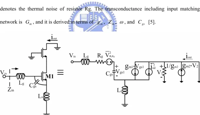
To estimate the noise figure of a cascode LNA, we take two dominate noise source for consideration. The thermal noise of the drain current from M1 and thermal noise of resistor Rg are estimated in our noise figure calculation. Fig. 2-7 shows the small signal model of the input stage, where 2
nd
i denotes the thermal noise of the drain current from M1 and Vn2,Rg
denotes the thermal noise of resistor Rg. The transconductance including input matching network is G , and it is derived in terms of m g , m Z , in ω , and C [5]. gs
Fig. 2-7 The equivalent noise and small signal model of the input matching network
gs in m m C j Z g G ω = (2.6)
15 j Q g C j R g G m in gs c s m m = ω = (2.7)
The input referred noise can be expressed as:
] 4 4 [ 1 | | 2 2 2 2 2 2 2 2 2 , m gs c s m g in m m out referred n kT g C R g kTR Q g G i v γ ω + = = (2.8)
Finally, the noise figure can be derived:
2 2 , 1 4 1 in s m s g s referred n Q R g R R kTR v NF = + = + + γ (2.9)
where γ is the body-effect coefficient. To have an insight into the effect influenced by the quality factor of Lg, QLg and the NF can be rewritten as:
g g c Lg R L Q =ω (2.10) 2 1 in s m s Lg g c Q R g R Q L NF = + ω + γ (2.11)
(2.11) clearly illustrates the degradation of poor quality factor of the input inductor
2.4.2.3 Power Dissipation
The power dissipation is also an issue for a LNA. The power dissipation is proportional to the designed inductors Lg and Ls, which can be derived as follow:
L W C V V V L W C V I P= D DD = μ ox ( GS − t)2 DD ∝μ ox 2 1 (2.12) where W is total width of input transistor, and L is 0.18um in this work. Using the input transistor’s gate-to-drain capacitance, Cgs, and (2.14), the (2.12) can be rewritten as (2.15).
ox gs WLC C 3 2 = (2.13) L W C gm ∝μ ox (2.14)
16 μ 2 2 L C g P gs m ∝ (2.15) By (2.3) and (2.4), we get ) 1 ( 1 ] ) ( [ ) ( 1 ) ( 3 2 2 2 2 2 2 s g s c g s g s c s g s L L L R R L L L L R R L P + − = + − ∝ ω μ ω μ (2.16)
To have an insight of the effect of Q , (2.16) is rewritten as: in
) 1 ( ) ( 3 2 2 2 4 2 2 s g s in s g s ox L L L Q R R R L W C P + − ∝ μ (2.17)
2.4.2.4 The Switched Dual-Band LNA Design Consideration
The switched dual-band LNA provides high amplification of the signals in the desired dual bands to reduce the effect of the following high noise stages and it presents low noise figure in the first stage in the receiving chain. Fig. 2-8 shows the proposed switched dual-band LNA. M1 and M2 are input transistors of the LNA. M1 is used for 2.45-GHz band, and M2 is used for 5.2-GHz band. When the LNA operates in one band, the other one is disabled by turning the corresponding input transistor off. The matching network is similar to a single band cascade LNA, and the design method is illustrated in last section. Since there are two input transistors in the dual-band LNA, the input matching network can be independently optimized for each band.
17
Fig. 2-8 The schematic of the proposed dual-band LNA
The switched resonator is composed of Ld1, Ld2, M7, Rg and Rd. The band selection of the LNA is performed by turning the PMOS M7 on/off. The control voltage, Vctl, applied to the PMOS M7 through a resistor Rg. Fig. 2-9 shows that when Vctl is 1.8V, and the PMOS, M7, is turned off. The Ld2 path exhibits high impedance. Thus the output resonator is dominated by Ld1 and Rd. Design Ld1 to let the output matching network resonate at 2.45-GHz. Fig. 2-10 shows that when Vctl is 0V, and M7 is turned on at triode region, and M7 exhibits its channel resistance (Ron). Thus the output resonator is dominated by Ld1 parallel with Ld2, and Ld2 is designed to keep the output matching network resonate at 5.2-GHz.
Fig. 2-9 M7 is off and the parasitic capacitance, CM7, provides a high reactance at 2.45-GHz.
18
Fig. 2-10 M7 is on and provides a turn on resistance Ron at 5.25-GHz.
There exists several types of variable gain LNA solutions in the literature (e.g. [14] ~[17]): They include: i) The variance of gate bias of the common gate MOS. The gain tuning range will be limited by biasing the common gate MOS in off region and the power consumption can not be economized at low gain mode. ii) A switching control type which provides gain controllability by switching on/off active gain components. The gain control range is limited by switching the active gain components in linear region. iii) The two-stage LNA-VGA type, which achieves gain control through the use of a VGA as a second stage. This additive gain-control functionality comes at a price of higher circuit complexity, which also results in an increase in power consumption and noise degradation.
In this work, we propose a novel gain control scheme. The gain control scheme can be performed by lowering the transconductance, gm, of the input transistor. However, lowering gm definitely causes the input impedance differ from Rs and the input equivalent tank will not resonate in the desired band anymore. Therefore, a new compensation method is proposed to overcome this shortage. The cascode transistor in the traditional LNA prototype is now extended to four shunted transistors. As shown in Fig. 2-8, M3~M6 are the compensative transistors in this gain control scheme. The gain control scheme provides four gain modes to adapt to the RF signal power and behaves the best communication quality. The gain control
19
signals are controlled by the base band and shown in Table 3
Vbias1 Vbias2 Mode1 0.65 0.70 Mode2 0.59 0.62 Mode3 0.55 0.55 Mode4 0.52 0.53 b1 b2 b3 b4 Mode1 1.8 1.8 1.8 1.8 Mode2 0 1.8 1.8 1.8 Mode3 0 0 1.8 1.8 Mode4 0 0 0 1.8 Table 3 Gain control signal from base band
While the RF signal power is large enough to saturate the blocks of the receiver, the baseband will sense the failure of receiving signals and sends a control signal to the gain controllable LNA. The multiple gain modes are required for the consideration of adapting to the unpredictable RF signal power. In this work, four gain control modes are planed and the gain tuning range 11.5 dB has been measured. IIP3 is the more significant parameter to identify the gain control scheme is beneficial to the receiver. The IIP3 improvement supports the LNA to adapt to the higher power signals and preserve the following blocks from saturation. The general gain tuning range is about 10 dB and it follows 10 dB IIP3 improvement. In this project, this principle has been accomplished.
2.4.3
Switched Gm Sub-Harmonic Mixer
A new prototype of sub-harmonic mixer suitable for 5.2-GHz ISM band is designed and implemented in a standard 0.18um CMOS technology. By the PMOS active load and a switched Gm prototype at LO port, the new sub-harmonic mixer achieves high conversion gain but still remain high linearity. The fully integrated sub-harmonic mixer achieves high conversion gain of 12.8dB, -1.8 dBm IIP3, and 14.0 dB noise figure at 10-MHz with 4 dBm LO power. Moreover, the proposed sub-harmonic mixer doesn’t consume dc power while there is no LO power.
20
2.4.3.1 Review of The Gilbert Mixer & Sub-Harmonic Mixer
Fig. 2-11 A basic Gilbert Mixer and the waveforms of output IF current
The double balanced or Gilbert-cell mixer in Fig. 2-11 is most desirable for high port-to-port isolation and spurious output rejection applications [4]~[6]. It can provide high conversion gain and low noise figure. The linearity is reasonably good. There are many design considerations about conversion gain, linearity and noise figure for a Gilbert mixer [25]. Here we only verify that the frequency conversion is attainable. By the waveform shown in Fig. 2-11, the output IF current, Iifp, can be thought of as the superposition of IA andIB.We can
simply model the switching on/off as a square wave and the RF signal as cosine based wave with amplitude A . The down conversion principle is derived as follow:
...}] ] 5 sin[ 5 1 ] 3 sin[ 3 1 ] {sin[ 2 2 1 )[ cos( − + + + = A t t t t Iifp rf ωLO ωLO ωLO π ω LO LO LO 1 2 1 1
cos( )[ {sin[ ( )] sin[3 ( )]} sin[5 ( )]+...}]
2 3 5 rf LO LO LO A ω t π ω t π ω t π ω t π π ω ω ω + + − + + + + + (2.18) 2
cos( rf ){(sin[ LO ] sin[ LO( )]) LO A ω t ω t ω t π π ω = − − + 1 (sin[3 ] sin[3 ( )]) 3 LO LO LO t t π ω ω ω + − + 1 (sin[5 ] sin[5 ( )]) 5 LO LO LO t t π ω ω ω + − + +...} (2.19)
21
2 2
cos( ){2cos[ ]sin[ ]
2 2 LO rf t A ω t ω π π π + = − − 6 3 2 3 cos[ ]sin[ ] 3 2 2 LOt ω + π π + − 10 5 2 5 cos[ ]sin[ ] 5 2 2 LOt ω + π π + − +...} (2.20) 1,3,5 2 2 2
cos( ) {cos[ ( )]sin[ ]}
2 2 LO rf n t n A t n n ω π π ω π ∞ = + = −
∑
− (2.21) 2 6 3 10 5 4 1 1cos( ){ cos[ ] cos( ) cos( ) ...}
2 3 2 5 2 LO LO LO rf t t t A ω t ω π ω π ω π π + + + = − − + − + (2.22) 4 1 1
cos( ){sin( ) sin(3 ) sin(5 ) ...}
3 5 rf LO LO LO A ω t ω t ω t ω t π = − + + + (2.23) 2 {(sin[( rf LO) ] sin[( rf LO) ]) A ω ω t ω ω t π = − + − − 1 (sin[( 3 ) ] sin[( 3 ) ]) 3 ωrf ωLO t ωrf ωLO t + + − − 1 (sin[( 5 ) ] sin[( 5 ) ]) 5 ωrf ωLO t ωrf ωLO t + + − − +...} (2.24) 1,3,5 2 {sin[( rf LO) ] sin[( rf LO) ]} n A n t n t nπ ω ω ω ω ∞ = =
∑
− ⋅ − + ⋅ (2.25)Eq. (2.25) shows the Gilbert mixer can execute frequency down conversion. The derivation demonstrated above will repeat for sub-harmonic mixer and we compare the difference of frequency translation between Gilbert mixer and sub-harmonic mixer.
22
Fig. 2-12 Traditional sub-harmonic mixer and waveforms of output IF current
The sub-harmonic mixing method is originally used in microwave circuits. The method uses a LO excitation with quadrature phase operating at a fraction of RF frequency [28]. The traditional sub-harmonic mixers can be implemented based on poly-phase LO switching, however, the circuit don’t have enough voltage headroom. Therefore, they aren’t suitable for voltage scaling down [29]. As shown in Fig. 2-12, the gate bias of the NMOS in the LO switching stage must be biased at least 1V for IIP3 well above 0dBm of a 10dB conversion gain [27]. The conventional method of operating the switching transistors at LO port in saturation region requires significant voltage headroom, thus, reducing the head room available for the load and hence limiting the achievable conversion gain. The tradition sub-harmonic mixer is similar to the basic Gilbert mixer, but the LO switching stage is driven by a quadrature LO signal such that only half of the RF frequency is needed for LO to down convert the RF signal. The RF transconductor stage translates the voltage signal to current signal by transconductance, gm. By the waveform shown in Fig. 2-12, the output IF current,
ifp
I , can be thought of as superposition of currents IA andIB. The down conversion principle of traditional sub-harmonic mixer is derived as follow:
1 2 1 1
cos( )[ {sin[2 ] sin[6 ] sin[10 ] ...}]
2 3 5
rfp rf LO LO LO
I A ω t ω t ω t ω t
π
23
1 2 1 1
cos( )[ {sin[2 ( )] sin[6 ( )] sin[10 ( )] ...}]
2 2 3 2 5 2 rf LO LO LO LO LO LO A ω t π ω t π ω t π ω t π π ω ω ω + + − + + + + + + (2.26) 2
cos( ){(sin[2 ] sin[2 ( )]) 2 rf LO LO LO A ω t ω t ω t π π ω = − − + 1 (sin[6 ] sin[6 ( )]) 3 LO LO 2 LO t t π ω ω ω + − + 1 (sin[10 ] sin[10 ( )]) 5 LO LO 2 LO t t π ω ω ω + − + +...} (2.27) 2 ]sin[ 2] 4 cos[ 2 ){ cos( 2 ω ω π π π − + − = A t LOt rf 2 ] 3 sin[ ] 2 3 12 cos[ 3 2 ω + π − π + LOt 2 ] 5 sin[ ] 2 5 20 cos[ 5 2 ω + π − π + LOt +...} (2.28) 2 ) ...} 5 20 cos( 5 1 ) 2 3 12 cos( 3 1 ] 2 4 cos[ ){ cos( 4 − + + + − + + − = ω ω π ω π ω π π t t t t A LO LO LO rf (2.29) 4 1 1
cos( ){sin(2 ) sin(6 ) sin(10 ) ...}
3 5 rf LO LO LO A ω t ω t ω t ω t π = − + + + (2.30) {(sin[( 2 ) ] sin[( 2 ) ]) 2 t t A ωrf ωLO ωrf ωLO π + − − − = 3(sin[( 6 ) ] sin[( 6 ) ]) 1 t t rf LO LO rf ω ω ω ω + − − + 5(sin[( 10 ) ] sin[( 10 ) ]) 1 t t rf LO LO rf ω ω ω ω + − − + +...} (2.31)
∑
∞ = ⋅ + − ⋅ − = 5 , 3 , 1 ]} ) 2 sin[( ] ) 2 {sin[( 2 n LO rf LO rf n t n t n A ω ω ω ω π (2.32)The down conversion principle can be understood distinctly by the derivated results. Comparing (2.32) with (2.25), the RF frequencies are down converted by a fundamental LO frequency and a 2nd harmonic LO one for Gilbert mixer and sub-harmonic mixer, respectively. By the derivation illustrated above, the operation of Gilbert mixer and sub-harmonic mixer
24
are understood and the new proposed switched Gm sub-harmonic mixer will be identified as the same operation.
2.4.3.2 Switched Gm Mixer
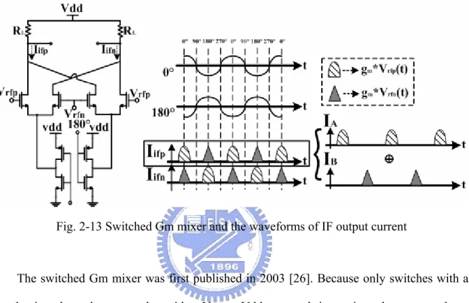
Fig. 2-13 Switched Gm mixer and the waveforms of IF output current
The switched Gm mixer was first published in 2003 [26]. Because only switches with a conductive channel connected to either Vss or Vdd are used, it requires almost no voltage headroom across the switch and does not require gate-drive voltages outside the supply rails. As a result, the gate-oxide stress of the switch devices is low, as desired for reliability concern. Even if oxide reliability is no issue, the conventional method of operating the switch transistors M2 and M3 in saturation requires significant voltage headroom, reducing the headroom available for the load and hence limiting the achievable conversion gain. By using low ohmic switches with a low-voltage drop compared to Vdd, almost the full supply voltage headroom can be reserved for the transconductance device and load, allowing for more conversion gain. By the time domain IF current plotting in Fig. 2-13, the same down conversion principle can be derived as (2.25). And the differential conversion gain can be obtained by multiplying 2gmRL to (2.25), that is:
25 L mR g CG π 4 = (2.33)
2.4.3.3 Proposed New Sub-Harmonic Mixer
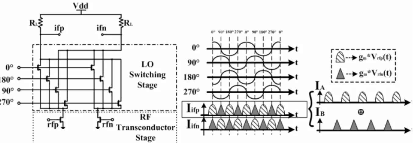
Fig. 2-14 Proposed switched Gm sub-harmonic mixer
Fig. 2-15 Waveform of the switched Gm sub-harmonic mixer
In this work, we combine a switched Gm technique at LO switching stage and a PMOS active load to implement a new sub-harmonic mixer that we can alleviate the shortage of the
26
voltage headroom at IF output [4]. Fig. 2-14 shows the topology of the new switched Gm sub-harmonic mixer. There are four inverters in the LO switching stage which are driven by a quadratue LO signal. Therefore, no power is consumed for this mixer while there is no LO input. Only one of the inverters can be activated to let either source of M1 and M2 or source of M3 and M4 be at low voltage.
By the same derivation as illustrated in the sub-harmonic mixer, the new sub-harmonic mixer has the same down conversion principle and it can be derived as follow:
] ) 2 sin( 2 2 1 )[ cos( ... 5 , 3 , 1
∑
∞ = − = n LO rf ifp n t n t A I ω π ω )]} 2 ( 2 sin[ 2 2 1 ){ cos( ... 5 , 3 , 1∑
∞ = + − + + n LO rf n t n t A ω π π π ω (2.34)∑
∞ = + = 5 , 3 , 1 ]} 2 sin[ )] 2 4 ( ){cos[ cos( 4 n LO rf n t n t n A ω ω π π π (2.35)∑
∞ = ⋅ + − ⋅ − = 5 , 3 , 1 ]} ) 2 sin[( ] ) 2 {sin[( 2 n LO rf LO rf n t n t n A ω ω ω ω π (2.36)Also the output IF current, I , can be derived in the same skill. And we can verify that the ifp maximum differential conversion gain of the new sub-harmonic mixer is
L mR g CG π 4 = (2.37)
However, the advantage of the sufficient voltage headroom at IF ports support the achievable conversion gain and keeps the mixer exhibits high linearity.
In (2.36), we can clearly identify that the proposed sub-harmonic mixer can down convert RF signal by operating the LO signal at half of the RF frequency. The maximum differential conversion gain is identical with the conventional one, but the noise and linearity is not the same case as illustrated in [27]. To acquire more conversion gain and keep the voltage head room sufficient, the PMOS active load is applied to the new sub-harmonic mixer. For measurement consideration, there are π matching networks in front of each RF and LO
27
signals. And a source follower is acted as the output buffer for the 50Ω system.
The finite ON-resistance of the switches may reduce the linearity and conversion gain of the switched Gm mixer, and this undesired effect must be estimated. We can model the switch with a finite ON-resistance, R , and it “allows” for source voltage variation. This voltage on can mix with the RF signal at the gate via the second-order term of the MOSFET, resulting in a differential output current:
3 1 2 2 3 1 ) 2 1 4 ( RF on on RF out v R g R g g v g i + − + = (2.38)
where g1,g2, and g are the Taylor series coefficients derived by taking the derivative of 3
d
I (V ) of the transconductor MOSFET. If the switch resistance is significantly lower than gs
1
/
1 g , the linearity can be better [27].
2.5 Measurement Consideration and Results
2.5.1
Switched Dual-Band LNA
2.5.1.1 Measurement Consideration
28
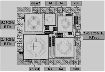
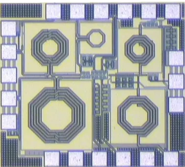
Fig. 2-17 The micrographic of the proposed switched dual-band LNA
The switched dual band LNA is designed for fully on-wafer measurement, therefore the arrangement of each pad must satisfy the probe station testing rules. By the layout shown in Fig. 2-16, two six-pin dc probes are required to feed with eight dc voltages. In addition, two RF probes are also needed for RF signals. Fig. 2-18 (a~b) shows the arrangement for dc and RF probes. The top and bottom are six-pin dc probes, while the left side is GSG RF probes for RF signal input and the right side is GSG RF probes for RF signal output.
The measurement equipments include a network analyzer ( HP8510C ), a noise analyzer ( Agilent N8975A ), a spectrum analyzer ( Agilent E4407B ), three signal generators, and several dc power supplies. Several auxiliary equipments are also required for the measurement setup, such as cables, 50Ω terminals, and power combiners. The losses of cables, combiners, and Baluns are all needed to be considered for calibration.
The S-parameter, noise figure, 1-dB compression point, IIP3 are needed to measure to verifying the switched dual-band LNA performance, and the measurement setups for each parameters are shown in Fig. 2-19 (a~c). We will show and discuss the measured results for each parameter.
29
(a) (b) Fig. 2-18 (a) On-wafer measurement test diagram(b) The photo for measurement environment
(a) (b)
(c)
30
2.5.1.2 Measurement Results and Discussion of Dual-Band LNA
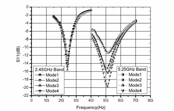
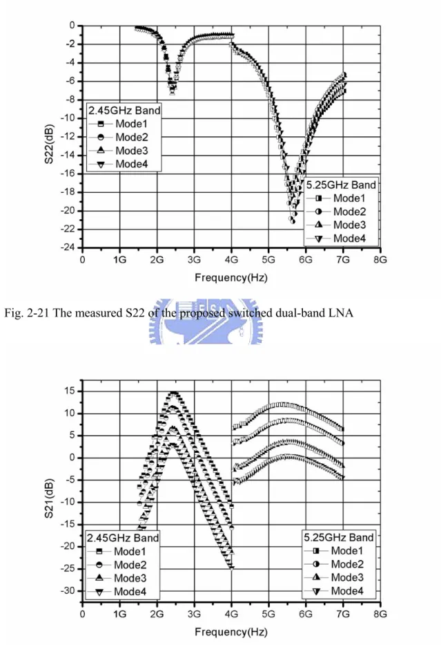
As shown in Fig. 2-20 to Fig. 2-23, the S-parameter of the four gain modes are “locked” in band and this is a benefit for a narrowband system such as 802.11a/b/g. For high gain mode, the measured S-parameter reveals 14.40 dB and 12.02 dB power gain, -12.18 dB and -11.02 dB input return loss, -6.73 dB and -12.09 dB output return loss, and -38.73 dB and -28.64 dB reverse isolation at 2.45-GHz and 5.25-GHz, respectively. For low gain mode, the power gain reduces to 3 dB and 0.18 dB at 2.45-GHz and 5.25-GHz, respectively.
The noise figure increases as the power gain switching form high gain mode to low gain mode. The measured noise figures for high gain mode are 3.54 dB and 2.88 dB at 2.45-GHz and 5.25-GHz, respectively. For low gain mode, the noise figure behaves 5.62 dB and 5.5 dB for 2.45-GHz and 5.25-GHz, respectively. The noise figure increments between high gain mode and low gain mode are 2.08 dB and 2.62 dB for 2.4-GHz and 5.2-GHz band, respectively. The noise figure increment is as expected even with about 11 dB gain tuning.
31
Fig. 2-21 The measured S22 of the proposed switched dual-band LNA
32
Fig. 2-23 The measured S12 of the proposed switched dual-band LNA
33
Fig. 2-25 The measured IIP3 at 2.4-GHz band of the proposed switched dual-band LNA
34
There are four gain modes for the proposed switched dual-band LNA, and the linearity improvement to adapting the higher input power must be considered. In the 5.2-GHz band, the measured IIP3 of the high gain mode is -16.4 dBm, and -4 dBm for low gain mode. A linearity improvement of 12.4 dB is achieved at 2.4-GHz band. On the other hand, the measured IIP3 of high gain mode and low gain mode in 5.2-GHz band are -0.8 dBm and 9 dBm, respectively. A linearity improvement of 9.8 dB is achieved in 5.2-GHz band.
2.5.1.3 Comparison with Other Literatures
This work combines two topics including switched dual-band and gain control ability, however, the published literatures discuss either dual-band or gain control ability. Hence, we compare these two topics independently, and comparison with dual-band LNA and gain controllable LNA are shown in Table 4 and Table 5, respectively.
Process Center Frequency Vdd S11/ S22(dB) S21(dB) NF (dB) IIP3(low gain) -IIP3(high gain) Power dispassion 2.45GHz -12.18 / -6.73 14.4 3.54 12.4dB 9.42mA This Work CMOS 0.18um 5.25GHz 1.8V -11.02 / -12.09 12.02 2.88 9.8dB 10.12mA 2.4GHz -10.1 / -10.5 10.1 2.9 6.5mA [7]2005 MWCL CMOS 0.18um 5.2GHz 1.8V -11.0 / -17.0 10.9 3.7 N/A 3.17mA 2.4GHz -5.1 / N/A 11.6@1V 8.5@0.7V 2.3 N/A [8]2003 ISCAS CMOS 0.18um 5GHz 1V/ 0.7V -26.3 / N/A 10.8@1V 5.5@0.7V 2.9 N/A 14.2mA @1V 6.2mA @0.7V 2.44GHz N/A 7.6 5.7 [9]2004 CMOS
0.18um 5.76GHz 1.8V N/A 8.6 6.8 N/A 6mA
Table 4 The comparison with published dual-band LNA
35
noise figure at high gain mode in 5.25-GHz band although the power consumption is the highest. However, the power consumption of this work is endurable in IEEE 802.11 a/b/g application. This Work (Meas.) [21]2005 IEE EL (Meas.) [22]2003 MWCL (Meas.) [23]2003 RFIC (Meas.) Process CMOS 0.18um CMOS 0.18um CMOS 0.18um CMOS 0.18um Center Frequency 2.45GHz 5.25GHz 5.7 GHz 5.7 GHz 5.75GHz Vdd 1.8V 1V 1.8V 1.8V S11/S22 (dB) -12.18/-6.73 -11.02/-12.09 -11.0 / -15.0 -15.0 / -9.0 >7 / N/A S21 (dB) 14.4 12.02 16.4 12.5 21.4 NF (dB) 3.54 2.88 3.5 3.7 4.4 NF(high gain)
-NF(low gain) 2.08 dB 2.62 dB 2.5 dB 1.8dB N/A Gain Tuning 11.4 dB 11.85 dB 8 dB 8.9 10.6 IIP3(high gain)
-IIP3(low gain) 12.4 dB 9.8 dB N/A N/A 12dB Power
Dispassion 9.42mA 10.12mA 3.2mA 8mA 9mA Table 5 The comparison with the published gain controllable LNA
In gain controllable LNA comparison, highest gain tuning range is presented in Table 5. The noise figure of this work in 5.25-GHz band is the lowest and linearity improvement is as expected while operating in low gain mode.
36
2.5.2
Switched Gm Sub-Harmonic Mixer
2.5.2.1 Measurement Consideration
The proposed sub-harmonic mixer is designed to down convert the 5.25-GHz differential signal, thus a Balun for 5.25-GHz is required to translate the RF signal into a differential signals. We use a Balun offered by CIC, and the Balun can operate at 5.25-GHz.
(a) (b) Fig. 2-27 (a) The LO port quadrature hybrid (b) The LO port rat-race
In addition, a quadrature 2.62-GHz signal is also necessary for the measurement of the sub-harmonic mixer. The method we adopt here is combining a quadrature hybrid shown in Fig. 2-27 (a) with two rat-races shown in Fig. 2-27 (b). Ideally the [S] matrix for the quadrature hybrid has the following form:
⎥ ⎥ ⎥ ⎥ ⎦ ⎤ ⎢ ⎢ ⎢ ⎢ ⎣ ⎡ − = 0 1 0 0 0 1 1 0 0 0 1 0 2 1 ] [ j j j j S (2.39)
To realize the operation of the four port device, we excite a unit of signal with desired frequency into port1 of the quadrature hybrid and else ports are terminated by 50Ω. The signal power will be evenly divided between port2 and port3, and a phase shift of 90° appears between these two ports. There is no power coupled to port4, and it is the isolation port. The
37
quadrature signal required in this project is accomplished by a quadrature hybrid and two rat-races illustrated above. The quadrature signals are connected to the LO switching stage shown in Fig. 2-14. We use the two ports vector network analyzer to identify the 90° phase shift of the fabricated quadrature Balun. Each ports are terminated by a 50Ω load except the measuring two ports. Fig. 2-28 shows the fabricated quadrature Balun and we measure its
21
S , S , 31 S41, S to verify 90° phase shift between port2 and port4. Furthermore, there 51
should be 180° phase shift between port2 (port4) and port3 (port5). The measured forward transmitted S-parameters for the quadrature balun are listed below:
° − ∠ =0.440 53.379 21 S ° ∠ =0.438 126.677 31 S ° − ∠ =0.450 146.00 41 S ° ∠ =0.449 36.811 51 S
Table 6 The measured forward transmitted S-parameter for each port
38
Fig. 2-29 The measured S-parameters for the fabricated quadrature Balun
39
The measured results show that the phase deviation less than 3° is achieved in the fabricated quadrature Balun. By the measured S-parameters, we can recognize that the fabricated quadrature Balun is suitable for our proposed sub-harmonic mixer. Fig. 2-29 and Fig. 2-30 show the magnitude in dB and phase of the measured results, respectively.
The layout of this sub-harmonic mixer is shown in Fig. 2-31, and Fig. 2-33 is the die photograph of the proposed switched Gm sub-harmonic mixer. Each bias is fed with the bonding wire connected to the prepared PCB test board except the “vdd” and “vddlo”. The bonding wire is estimated about 1nH per 1mm for the parasitic inductor, and the inductance must also be simulated with the proposed circuit. All the biases fed with bonding wires in our sub-harmonic mixer are gate biases, therefore, the variation of the estimated inductance for bonding wires cause less effect to our circuit’s performance. The PCB test board layout is shown in Fig. 2-32, and the IF differential ports are connected by bypass capacitors and SMA connectors. The selected IF here is 10MHz that the loss contributed by the PCB board and the SMA connector are negligible.
The simplified measurement setups are shown in Fig. 2-34 (a~d). The RF and LO signals are fed on wafer for elimination of undesired parasitic effects. Fig. 2-35 shows the PCB test board for this sub-harmonic mixer and the whole measurement environment in CIC.
Fig. 2-31 The layout of the proposed sub-harmonic mixer
Fig. 2-32 PCB test board layout of the sub-harmonic mixer
40
41
(a) (b)
(c) (d) Fig. 2-34 Measurement setup of the proposed switched Gm sub-harmonic mixer for (a) input return
42
(a) (b)
(c)
43
2.5.2.2 Measurement Results
By the measurement setups illustrated above, the measured results are listed below. The RF and LO measurement was performed on-wafer. The biases were fed with bonding wires. A quadratue LO signal source at 2.62-GHz was used. This new sub-harmonic mixer consumes no dc power while there is no LO signal input. The buffer consumes 12.42mA dc current from 1.8V power supply. Unfortunately, the measured current indicates that the process condition now falls at the vicinity of SS-corner. Therefore, the following measured results are compared with the SS-corner simulation. As shown in Fig. 2-36, the measured RF and LO input return loss are -17.2 dB at 5.25-GHz and -18.0 dB at 2.62-GHz. The input return losses are well matched to system impedance in both RF and LO inputs. In this work, a high differential conversion power gain, 12.8 dB is achieved (see Fig. 2-37). As can be seen, the maximum differential conversion power gain is happened at the LO power of 4 dBm..
Fig. 2-38 shows the DSB noise figure against the IF frequency. The LO signal is fixed to 2.62GHz, and RF signal sweep from 5.25GHz to 5.32GHz. The IF frequency we choose is 10-MHz for system integration and cost consideration [1]. The DSB noise figure is 14 dB at 10-MHz.
Finally, Fig. 2-39 shows the input 3rd order intercept point (IIP3) of -1.8 dBm. The linearity of the sub-harmonic mixer is well performed especially the mixer achieves high conversion gain.
The port to port isolation is also taken into consideration in the proposed sub-harmonic mixer. The isolation of the fundamental LO signals (2.62-GHz) to RF port and IF port are higher than 40 dB and 31 dB respectively. The more important is the second harmonic of the LO signal (5.24-GHz), and it performs higher than 67 dB and 52 dB for RF port and IF port respectively.
44
Fig. 2-36 The simulated and measured RF and LO return loss
45
Fig. 2-38 The simulated and measured DSB noise figure